Article

Contactless Determination of Electric Field in Metal–Insulator–Semiconductor Interfaces by Using Constant DC-Reflectivity Photoreflectance

1
Advanced Interdisciplinary Science and Technology, Graduate School of Engineering, University of Fukui, Fukui 910-8507, Japan
2
Department of Electric and Electronics Engineering, University of Fukui, Fukui 910-8507, Japan
3
Research Center for Development of Far-Infrared Region, University of Fukui, Fukui 910-8507, Japan
*
Author to whom correspondence should be addressed.
Submission received: 11 February 2021 / Revised: 11 March 2021 / Accepted: 21 March 2021 / Published: 29 March 2021
(This article belongs to the Special Issue Feature Papers of Solids 2021)

Abstract

:
We applied photoreflectance (PR) spectroscopy for contactless determination of the electric field strength at buried interfaces in metal–insulator–semiconductor (MIS) structures. The PR is an all-optical version of an electromodulated reflectance spectroscopy. The tradeoff of this adoption is that this requires an additional feedback system to eliminate background problems induced by scattered pump light and/or photoluminescence. A microcomputer-based feedback system has been developed for this elimination. Despite the very tiny signal intensity, we successfully attained a sufficiently good signal–noise ratio to determine the electric field strength in oxide-based MIS interfaces that exhibits a large, unwanted photoluminescence signal. The field strength was evaluated to be ca. 0.25 kV/cm.

1. Introduction

Modulation spectroscopy has played an important role in characterizing the optical properties of solids [1,2,3,4]. Due to its inherent derivative nature, the resultant spectrum becomes free from the broad background [5]. This spectroscopy has been mainly used for an electronic-band-structure characterization. As stated explicitly by Aspnes and coworkers [1,2], the electroreflectance (ER) can also detect, in principle, the Franz–Keldysh oscillation (FKO) as a result of the relatively strong built-in electric field despite its signal intensity—at least one order of magnitude smaller than the band-edge response [6,7,8].
Photorefletance (PR) is known to be one of such modulation spectroscopies [3,4]. Traditionally, external perturbations such as electric fields have been applied to measure differential reflectivity. In the case of PR, perturbation is implemented through an additional pump laser beam by modulating the built-in electric fields near the solid surfaces. Photo-absorbed electrons are excited, and the dielectric constant is resultingly changed in accordance with the change of the electronic distributions. Then, the change in the dielectric constant induces the change of the reflectivity. This spectroscopy has desirable attributes such as its non-destructive and contactless properties [9,10]. These are attractive for the contactless assessment of the interface properties such as electric field strength and Schottky barrier height because of its possibility of extension to the in situ diagnosis, which is compatible with the processing environments [11,12]. It should be noted that it is very difficult to accomplish in the cases of other kinds of contactless probes [13,14,15].
On the other hand, the PR has a drawback that is well-known as “the spurious signal problem” [16,17,18]. This is owing to the interfusion with photoluminescence (PL) or laser scattered light. Due to this, the detection limit of this spectroscopy seems to be worse than that of the ER spectroscopy. A look through the literature revealed that many works related to the detection of the FKO in wide-gap semiconductors have been mainly dedicated to multiple quantum wells, where the signal intensity was earned with the periodicity of the structures [19]. There are few works except for that in Au Schottky contacts on GaN [20]. A contactless characterization tool should preferably cover the basic device structures such as bulk-crystalline-based Schottky diodes and simple metal–insulator–semiconductor (MIS) structures. To suppress the spurious contribution and to enhance the detection limit, Shen and coworkers [16] proposed keeping the direct current (DC) component (Vdc) constant independent of the photon energy, enabling the facile a posteriori subtraction of the spurious signal contributions [17]. While this was originally termed a new normalization procedure, we rather call it a constant DC-reflectivity PR, in analogy with the constant photocurrent method [21]. Among many other methods previously proposed, this technique can most soundly balance between advantages and cost-effectiveness [18,22,23,24].
This paper describes a microcomputer-based implementation of the constant DC-reflectivity PR spectroscopy because obsolete electrical parts adopted in the original work [16] must have been replaced with the state-of-the-art counterparts. After explaining the design of our feedback system, we demonstrate how to efficiently maintain the constant DC component voltage (Vdc) with this. Finally, we report our observation of FKO in the PR spectrum taken for an oxide-based MIS structure that exhibits a large, unwanted PL signal. The interface electric field strength is also evaluated.

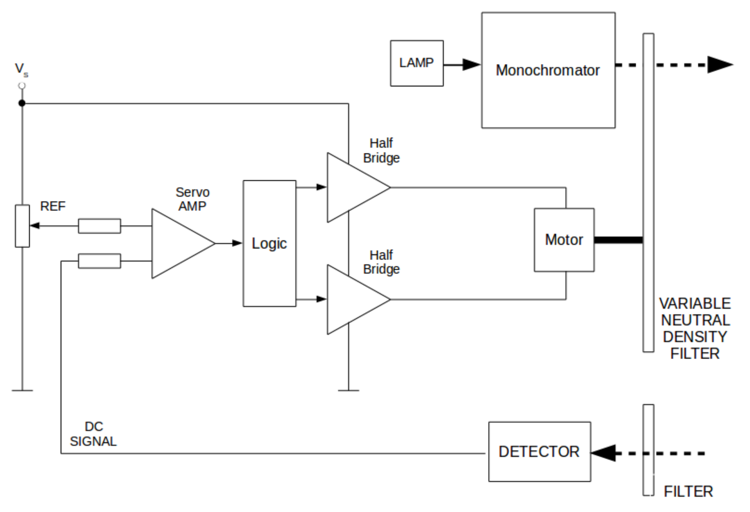
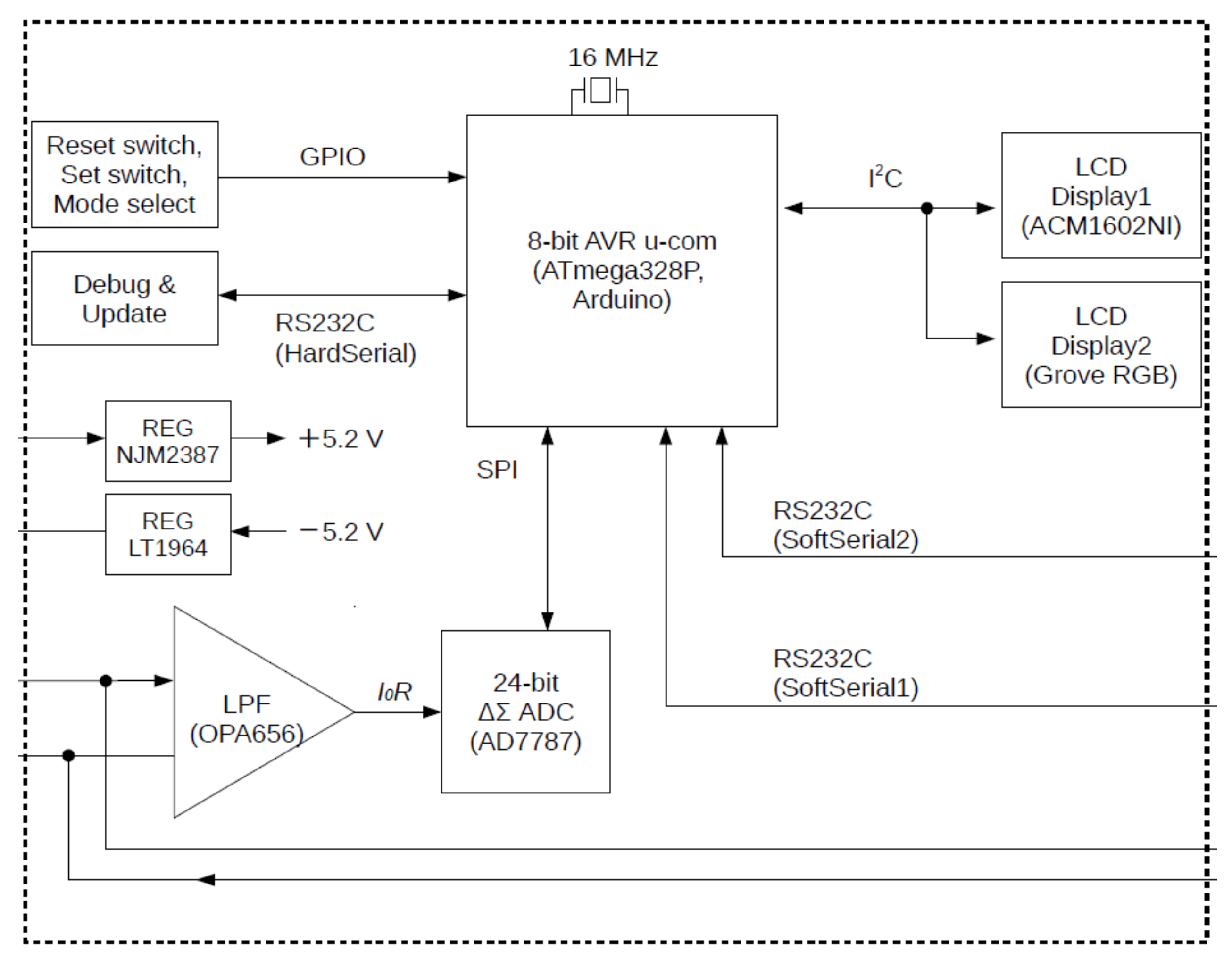
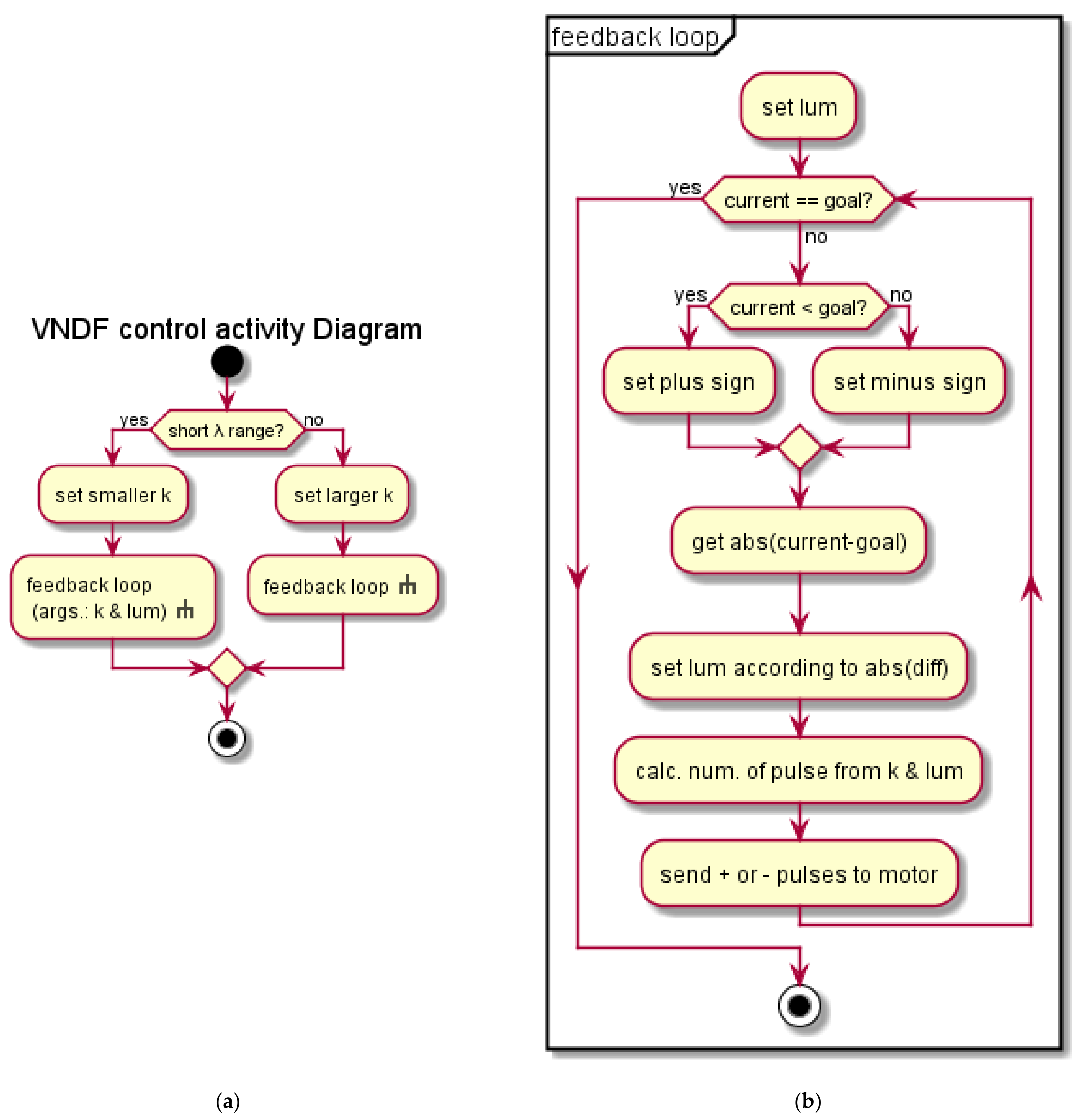
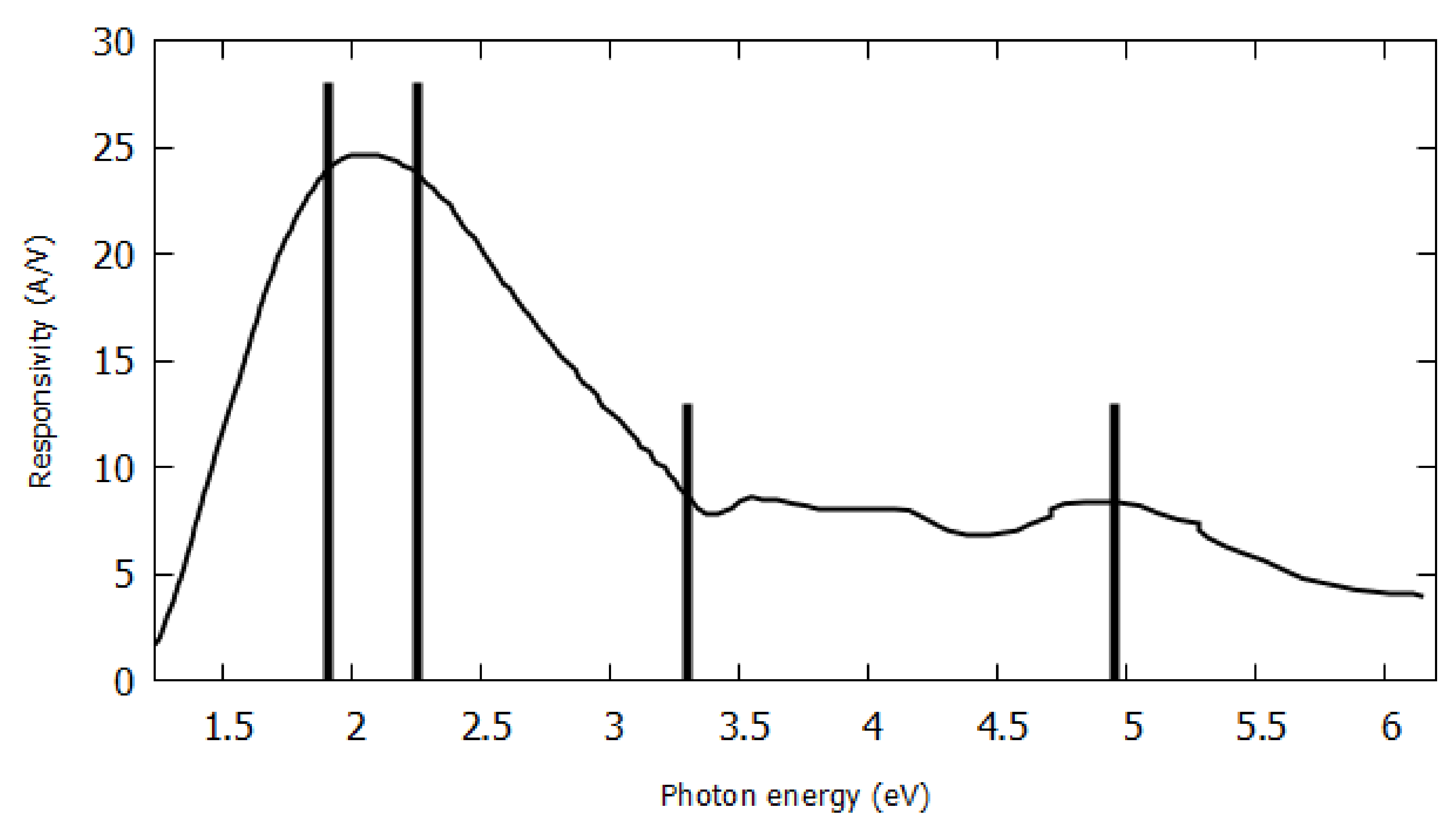
2. Experimental Procedures

As earlier stated, it is considered to be very difficult to detect tiny FKO-related signals without the extension to the conventional PR. This is especially true for the widegap-semiconductor-based simple Schottky or MIS diodes. It is impossible to reproduce the original set-up [16] with the electrical parts available nowadays. Therefore, let us explain our system in detail.
First, we explain why we normalized the DC reflectivity (Vdc) for the PR for the spurious signal suppression. Signals detected with the modulation spectroscopy include two components; i.e., Vdc and modulated AC components (Vac) [16]. The quantity that we wish to obtain is Vac divided by Vdc. A detailed explanation of the principle can be found elsewhere [16,23]. We only show the relevant equations below without introducing excessively complicated quantities. By letting E take photon energy, the DC output can be expressed as:
V d c = I 0 R E .
Here, I 0 denotes an effective input intensity that also accounted for gains of the avalanche photodetector (APD) and post-amplifier. In other words, I 0 is an inputting intensity multiplied by these gains.
On the other hand, spurious signals tend to contribute to the Vac in PR, and this reads:
V a c = I 0 Δ R E + I s p ,
where I s p denotes the intensity of spurious component that includes again the abovementioned gains. It should be noted that I s p is independent of the photon energy because of the dark configuration. In other words, this can be regarded as a constant.
Thus, the relationship between V d c / V a c and Δ R / R can be written as
V d c V a c E = I 0 Δ R E + I s p I 0 R E = Δ R E R E + I s p V d c .
The second term of Equation (3) becomes constant if the V d c E is independent of probe energy (E). That is why we wish to keep the Vdc irrespective of the photon energy. This facilitates an a posteriori subtraction of the spurious signal.
In the original approach [16], a variable neutral density filter (VNDF) mounted on a servo-motor was adopted to maintain constant Vdc. A VNDF is a filter that allows you to adjust the attenuation of the incoming light intensity. By rotating the filter, the filter shifts between low and high attenuations. The basic design of the servo-motor-based control system is shown in Figure 1. It is known that the precision in position determination of a stepping motor is superior to that of the servo motor. However, the control requirements of the stepping-motor drive are so unique that the concepts for the servo motors can hardly be extrapolated to those of the stepping motors. A driver for a stepping motor is usually controlled with a personal computer (PC), which tends to severely deteriorate the stability of the feedback systems due to the power-line noise. On the other hand, if this is controlled with a low-cost RISC (reduced instruction set computer) microcontroller, i.e., Arduino ATmega328P, it also enables stability attainable with the battery power feeding.
Next, we explain our proposed designs on the algorithm and circuits for the stepping motor drive system, which is power-delivered from the DC batteries, as shown in Figure 2. We drove this stepping motor by using a stage controller (PAT-001, Sigma Koki Co. Ltd., Tokyo, Japan). The power driving source is a lead-acid battery. We developed an original circuit for the RISC control. For the feedback, the pulse number sending to the stepping motor was adjusted following the distance between the present and target values (otherwise known as Vdc) [25].
Next, we describe the algorithm of our proposed design. Figure 3 shows a flow chart of our feedback system. We used the Arduino language, which is similar to the C/C++ language, for coding. As shown in the right-hand side panel of Figure 3, we determined the sign of the number of pulses, depending on the positive/negative in the difference between current DC reflectivity and the target Vdc. Additional care has to be taken if an APD is used as a detector instead of a photo-multiplier tube. As shown in Figure 4, there is a relatively large variation in its sensitivity curve especially in the UV range. As earlier stated, our main target is related to the wide-gap semiconductors. Therefore, we decided on mutual communication between the RISC and the monochromator. To minimize the influence of the PC noise, we used a universal photocoupler (TLP785) and added an isolated communication circuit to the communication path between the VNDF control unit and a PC. We ensured electrical isolations between the VNDF and the PC, while the bidirectional communication was implemented. We set the baud rate down to 1200 bps (bit per second) to avoid unfaithful waveform transform and the resulting communication errors. As shown on the left-hand side of Figure 3, the RISC controller inquires about the current photon energy before calling the subroutine for the feedback control. Then, we calculate the absolute number of the pulse sending to the motor by introducing two following empirical parameters, i.e., k and lum, respectively. Since the sensitivity of the APD significantly depends on the photon energy, the Vdc change per the density-filter angle also depends on the energy. The parameter k takes this effect into account. Then, we divided the sensitivity curve of the APD into five regions, as shown by the vertical lines in Figure 4. We have performed the linear regression analysis for each region to determine the slopes. The value of k was finally calculated from the absolute value of the slopes of the sensitivity curve. To avoid the so-called overshooting behavior, we introduced an additional empirical parameter lum. This parameter was decided by the difference between the current value and the target Vdc. The adjustment method of this parameter is similar to the parameter p in the PID (proportional–integral–derivative) language. By accounting for the above-mentioned parameters, we calculated the number of pulses (Npuls) according to the equation: Npuls = k × lum. It should be noted that we rounded Npuls to make the number integer only. We repeated such feedback until the convergence. The convergence was judged if the difference falls within acceptable limits, i.e., ±1% of the target Vdc. In the case of the APD PR spectroscopy for the near UV region, our algorithm allowed us to result in more secure convergence rather than the use of the PID subroutine equipped by the Arduino library.
Finally, we explain our optical set-up and device under test (DUT). We adopted what is often called a dark configuration, i.e., the monochromatized probe beam fed onto the DUT. As a chopped pump beam, we used 325-nm-line from an HeCd laser. The reflected probe beam was focused on the APD. Irises were placed in our optical path to limit the acceptance angle [26]. While the PL angular distribution follows Lambert’s cosine law, the directionality of the reflectance is superior to that of PL. The iris insertion technique can block the PL signals, thereby drastically reducing the collection efficiency of PL signals, i.e., the spurious contribution. As long as an Xe arc lamp is used as a probe source, this technique is not sufficient to completely suppress the spurious contribution. Despite its incompleteness, this helped the efficiency and precision of our constant DC-reflectivity PR. The DUT is a ZnO-based MIS structure. We introduced additional stacking layers of several-nm-thick Al2O3 and semitransparent gold on a commercially available ZnO crystal using the atomic layer deposition technique. The DUT was attached to a cold finger of a refrigerator for cryogenic temperature measurement.

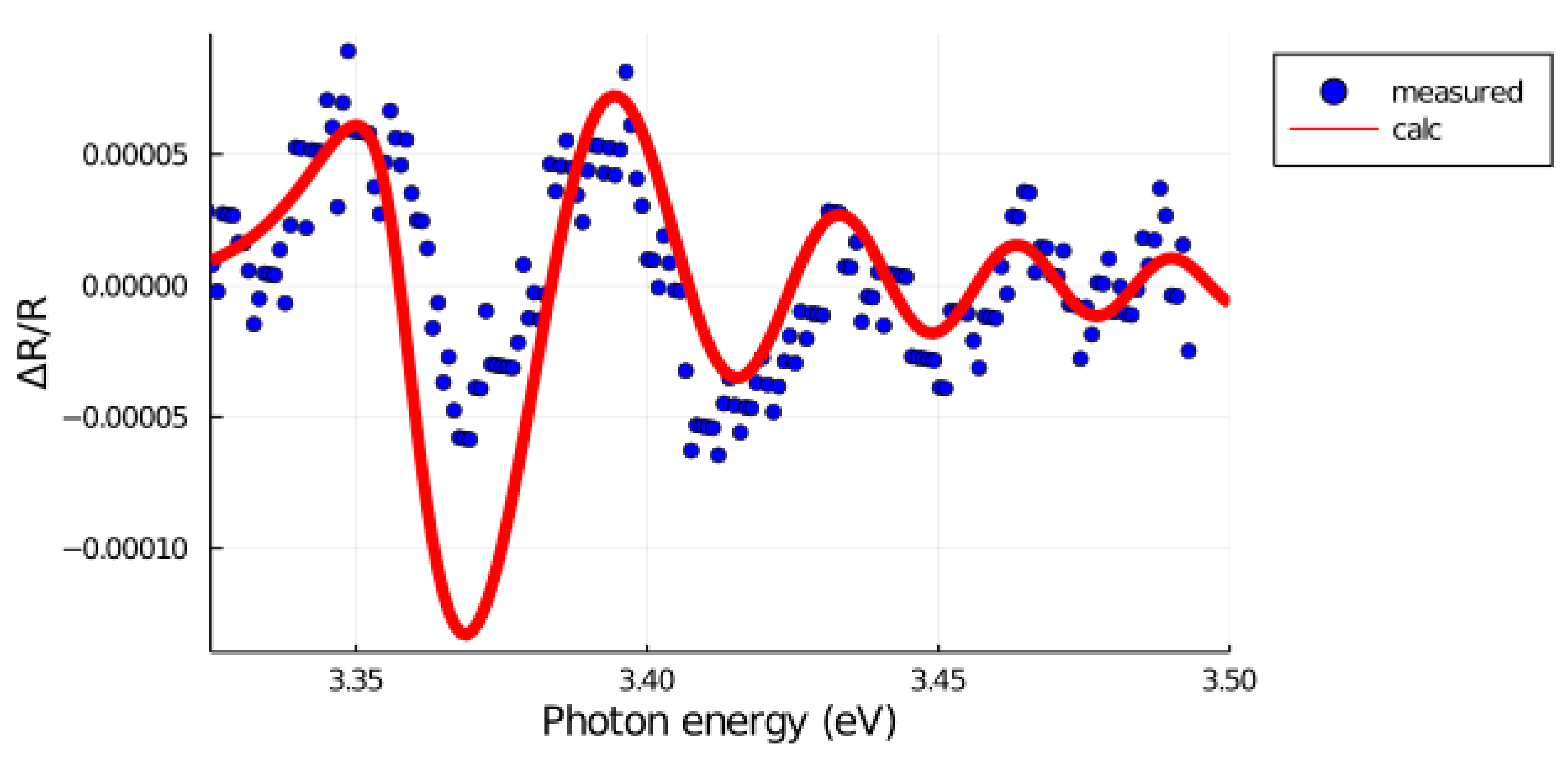
3. Experimental Results and Discussion

Figure 5 shows the Vdc(E) spectra with using the VNDF control. The target Vdcs are 300, 750, 1000, 2500, and 3500 mV, respectively. As can be understood from Figure 5, it can be said that we successfully control the feedback with the various Vdc values. Moreover, this control system attained good performance on reproducibility.
Having established our PR scheme, we measured a PR spectrum for the ZnO-based MIS structure [27,28]. Figure 6 shows the differential reflectivity spectrum (closed circles) using the VNDF. The measurement temperature is approximately 180 K. The spurious signal subtraction has been made already to show this datum. A calculated result using Equation (2) of Ref. [29] is shown with a solid line. In addition to the excitonic anomaly (at approximately 3.35 eV), we can also observe an oscillatory structure above this resonance energy [30,31]. This observation suggests a strong-field regime [1,2]. The electric field is concentrated near the interface of this MIS structure [32,33,34]. The distortion of the PR lineshape from that in the low-field regime suggests that the higher energy signal can be assigned to the FKO [6,7,8,35,36,37]. For the analysis, we adopted the theory by Aspnes [1,2], the functional forms of which were concisely formulated in Equation (2) of Ref. [29]. We adjusted the relevant parameters to reproduce the behavior of observed FKO while sacrificing the coincidence around the excitonic anomaly (at 3.35 eV). We believe that the signal-to-noise ratio here is sufficiently high enough to be able to determine the energies of nodes and antinodes of the FKO. This may be justified if we consider the fact that the FKO signal is generally tiny, especially in the case of the wide-gap semiconductors. The value of Vdc for this measurement was 750 mV. While the slight increase in this quantity allowed the observation of the FKO, the distortion of the waveform became severe at the Vdc levels greater than 2.5 kV.
Hereafter, we explain how to evaluate the electric field strength from the FKO. From the oscillating period, a parameter Θ was determined to be ca. 0.021 eV. By letting me take the electron effective mass, the electric field F is related with Θ through F2 = 2me Θ3/(eħ)2. Nomenclatures other than me have their standard meanings. Since the electron mass of ZnO is 0.23 m0 [38], then the electric field was evaluated to be ca. 0.25 kV/cm, which is in the same order of magnitude as the case of the Schottky contact on GaN. The values are Θ ≅ 0.04 eV, and me = 0.22 m0, respectively. It should be noted that the energetic determination of the nodes and antinodes enables the quantification of the electric field strength without the model regression analysis, as has been performed in Ref. [20].
Finally, we mention the discrepancy at the excitonic resonance. Although the reason for this discrepancy is not clear at moment, this is attributed to the fact that the present model is based on the standard-critical-point (SCP) theory. The existence of the strong built-in electric field tends to screen the Coulomb force between an electron and a hole, resulting in an excitonic instability [39]. Probably, such an unstable exciton cannot be correctly modeled in the framework of the SCP model [3,4,5].

4. Conclusions

For the contactless determination of the interface electric field, we have customized PR spectroscopy unaffected by unwanted spurious signals. We describe state-of-the-art electronics implementation to vary the intensity of the probe beam to maintain a constant Vdc instead of the traditional servomechanism. This accomplishment provides a cost-effective solution based on microcomputers for constant DC-reflectivity PR spectroscopy. This system can be assembled easily because they consist of versatile electronic parts that are often used in controlling circuits nowadays. The advantage of our method has been demonstrated on a ZnO-based MIS structure that exhibits a large, unwanted PL signal. The electric field strength was also evaluated. It is expected that this can be also applied to the spectroscopies other than the PR such as the constant photocurrent method [21].

Author Contributions

Conceptualization, E.K. and T.M.; methodology, E.K.; software, E.K.; validation, E.K., K.S. (Koya Satta) and K.S. (Ken Suzuki); measurements, K.S. (Koya Satta), R.I., K.S. (Ken Suzuki); writing, T.M., E.K.; visualization, T.M., E.K., K.S. (Koya Satta), R.I.; supervision, T.M.; project administration, T.M.; funding acquisition, T.M. All authors have read and agreed to the published version of the manuscript.

Funding

This research was funded by the Ministry of Education, Culture, Sports, Science and Technology, grant number KAKENHI-19K05303.

Institutional Review Board Statement

Not applicable.

Informed Consent Statement

Not applicable.

Data Availability Statement

The data presented in this study are available on request from the corresponding author. The data are not publicly available due to privacy.

Acknowledgments

Technical assistance from H. Yamamori from the University of Fukui is acknowledged. Atomic layer deposition was performed in Tohoku University, Japan. We acknowledge the permission of its machine time. We acknowledge the scientific contribution from A. Hashimoto (University of Fukui).

Conflicts of Interest

The authors declare no conflict of interest.

References

  1. Aspnes, D.E. Third-Derivative Modulation Spectroscopy with Low-Field Electroreflectance. Surf. Sci. 1973, 37, 418. [Google Scholar] [CrossRef]
  2. Aspnes, D.E.; Studna, A.A. Schottky-Barrier Electroreflectance: Application to GaAs. Phys. Rev. B 1973, 7, 4605. [Google Scholar] [CrossRef]
  3. Pollak, F.H. Modulation Spectroscopy as a Technique for Semiconductor Characterization. Proc. SPIE 1981, 276, 142. [Google Scholar] [CrossRef]
  4. Pollak, F.H.; Glembocki, O.J. Modulation Spectroscopy of Semiconductor Microstructures: An Overview. Proc. SPIE 1988, 946, 2. [Google Scholar] [CrossRef]
  5. Pollak, F.H.; Shen, H. Modulation Spectroscopy of Semiconductors: Bulk/Thin Film, Microstructures, Surfaces, Interfaces and Devices. Mater. Sci. Eng. R 1993, 10, 275. [Google Scholar] [CrossRef]
  6. Franz, W. Einfluss Eines Elektrischen Feldes Auf Eine Optische Absorptionskante. Z. Naturforsch. 1958, 13a, 484. [Google Scholar] [CrossRef]
  7. Keldysh, L.V. The Effect of a Strong Electric Field on the Optical Properties of Insulating Crystals. Sov. Phys. JETP 1958, 7, 788. [Google Scholar]
  8. Ralph, H.I. On the Theory of the Franz-Keldysh Effect. J. Phys. C 1968, 1, 378. [Google Scholar] [CrossRef]
  9. Qin, J.; Huang, Z.; Ge, Y.; Hou, Y.; Chu, J. Tandem Demodulation Lock-in Amplifier Based on Digital Signal Processor for Dual-Modulated Spectroscopy. Rev. Sci. Instrum. 2009, 80, 033112. [Google Scholar] [CrossRef] [PubMed]
  10. Yan, D.; Qiang, H.; Pollak, F.H. A New Offset Technique for Suppression of Spurious Signals in Photoreflectance Spectra. Rev. Sci. Instrum. 1994, 65, 1988. [Google Scholar] [CrossRef]
  11. Acher, O.; Omnes, F.; Razeghi, M.; Drevillon, B. In Situ Characterization by Reflectance Difference Spectroscopy of III-v Materials and Heterojunctions Grown by Low Pressure Metal Organic Chemical Vapour Deposition. Materials Sci. Eng. B 1990, 5, 223. [Google Scholar] [CrossRef]
  12. Yasuda, T. In Situ Characterization of ZnSe/GaAs Interfaces by Reflectance Difference Spectroscopy. J. Vacuum Sci. Technol. B Microelectron. Nanometer Struct. 1996, 14, 3052. [Google Scholar] [CrossRef]
  13. Yin, X.; Pollak, F.H. Novel Contactless Mode of Electroreflectance. Appl. Phys. Lett. 1991, 59, 2305–2307. [Google Scholar] [CrossRef]
  14. Motyka, M.; Kudrawiec, R.; Sek, G.; Misiewicz, J.; Bisping, D.; Marquardt, B.; Forchel, A.; Fischer, M. Contactless Electroreflectance Investigation of Energy Levels in a 1.3 Micron Emitting Laser Structure with the Gain Medium Composed of InAsN Quantum Dots Embedded in GaInNAs/GaAs Quantum Wells. Appl. Phys. Lett. 2007, 90, 221112. [Google Scholar] [CrossRef]
  15. Lin, H.; Braeuninger-Weimer, P.; Kamboj, V.S.; Jessop, D.S.; Degl-Innocenti, R.; Beere, H.E.; Ritchie, D.A.; Zeitler, J.A.; Hofmann, S. Contactless Graphene Conductivity Mapping on a Wide Range of Substrates with Terahertz Time-Domain Reflection Spectroscopy. Sci. Rep. 2017, 7, 10625. [Google Scholar] [CrossRef] [Green Version]
  16. Shen, H.; Parayanthal, P.; Liu, Y.F.; Pollak, F.H. New Normalization Procedure for Modulation Spectroscopy. Rev. Sci. Instrum. 1987, 58, 1429. [Google Scholar] [CrossRef]
  17. Qiang, H.; Yan, D.; Yin, Y.; Pollak, F.H. Characterization of Semiconductor Device Structures by Modulation Spectroscopy. Proc. SPIE 1994, 2141, 58. [Google Scholar] [CrossRef]
  18. Li, Q.; Tan, H.H.; Jagadish, C. A New Optical Front-End Compensation Technique for Suppression of Spurious Signal in Photoreflectance Spectroscopy Using an Antiphase Signal. Rev. Sci. Instrum. 2010, 81, 043102. [Google Scholar] [CrossRef]
  19. Wetzel, C.; Takeuchi, T.; Amano, H.; Akasaki, I. Piezoelectric Franz-Keldysh Effect in Strained GaInN/GaN Heterostructures. J. Appl. Phys. 1999, 85, 3786. [Google Scholar] [CrossRef] [Green Version]
  20. Liu, W.; Li, M.-F.; Chua, S.-J.; Akutsu, N.; Matsumoto, K. Photoreflectance Study of Au-Schottky Contacts on n-GaN. J. Electron. Mater. 1999, 28, 360. [Google Scholar] [CrossRef]
  21. Hattori, K.; Fukuda, S.; Nishimura, K.; Okamoto, H.; Hamakawa, Y. Interpretation of CPM Measurements in Amorphous Semiconductors. J. Non-Cryst. Solids 1993, 164, 351. [Google Scholar] [CrossRef]
  22. Kita, T.; Yamada, M.; Wada, O. Dual Chopped Photoreflectance Spectroscopy for Nondestructive Characterization of Semiconductors and Semiconductor Nanostructures. Rev. Sci. Instrum. 2008, 79, 046110. [Google Scholar] [CrossRef] [Green Version]
  23. Liao, Y.F.; Chang, C.C.; Wang, D.P.; Tseng, B.H.; Liao, Y.D.; Lin, C.H. A Novel Approach for Normalizing the Photoreflectance Spectrum by Using Polymer-Dispersed Liquid Crystal. Rev. Sci. Instrum. 2012, 83, 103904. [Google Scholar] [CrossRef] [PubMed]
  24. Misiewicz, J.; Sitarek, P.; Sek, G.; Kudrawiec, R. Semiconductor Heterostructures and Device Structures Investigated by Photoreflectance Spectroscopy. Mater. Sci. 2003, 21, 263. [Google Scholar]
  25. Kobayashi, E.; Shimmura, S.; Ito, S.; Makino, T. A New Photoreflectance Signal Possibly Due to Midgap Interface States in Buried f-Doped SnO2/TiO2 Junctions. Jpn. J. Appl. Phys 2019, 59, SCCB23. [Google Scholar] [CrossRef]
  26. Zhang, B.; Wang, X.-J. Note: A Modified Optics Based Technique for Suppressing Spurious Signals in Photoreflectance Spectra. Rev. Sci. Instrum. 2017, 88, 106103. [Google Scholar] [CrossRef] [PubMed]
  27. Ozgur, U.; Alivov, Y.I.; Liu, C.; Teke, A.; Reshchikov, M.A.; Dogan, S.; Avrutin, V.; Cho, S.J.; Morkoc, H. A Comprehensive Review of ZnO Materials and Devices. J. Appl. Phys. 2005, 98, 041301. [Google Scholar] [CrossRef] [Green Version]
  28. Klingshirn, C. ZnO: From Basics Towards Applications. Phys. Status Solidi B 2007, 244, 3027. [Google Scholar] [CrossRef]
  29. Ando, M.; Nakayama, M.; Nishimura, H.; Schneider, H.; Fujiwara, K. Franz-Keldysh Oscillations at the Miniband Edge in a GaAs Superlattice. Superlat. Microstr. 1997, 22, 459. [Google Scholar] [CrossRef]
  30. Makino, T.; Chia, C.H.; Tuan, N.T.; Segawa, Y.; Kawasaki, M.; Ohtomo, A.; Tamura, K.; Koinuma, H. Exciton Spectra in ZnO Epitaxial Layers on Lattice-Matched Substrates Grown with Laser-Molecular-Beam Epitaxy. Appl. Phys. Lett. 2000, 76, 3549. [Google Scholar] [CrossRef]
  31. Ozaki, S.; Mishima, T.; Adachi, S. Photoreflectance Spectroscopy of ZnO for Ordinary and Extraordinary Rays. Jpn. J. Appl. Phys 2003, 42, 5465. [Google Scholar] [CrossRef]
  32. Sze, S.M. Physics of Semiconductor Devices; Wiley: New York, NY, USA, 1981; ISBN 0471056618. [Google Scholar]
  33. Baenard, W.O.; Myburg, G.; Auret, F.D.; Goodman, S.A.; Meyer, W.E. Metal Contacts to Gallium Arsenide. J. Electron. Mater. 1996, 25, 1695. [Google Scholar] [CrossRef]
  34. Hall, D.J.; Hosea, T.J.C.; Lancefield, D. Airy Function Analysis of Franz-Keldysh Oscillations in the Photoreflectance Spectra of Layers. J. Appl. Phys 1997, 82, 3092. [Google Scholar] [CrossRef]
  35. Ashok, S.; Borrego, J.M.; Gutmann, R.J. Electrical Characteristics of GaAs MIS Schottky Diodes. Solid-State Electron. 1979, 22, 621. [Google Scholar] [CrossRef]
  36. Hughes, P.; Weiss, B.; Hosea, T. Analysis of Franz-Keldysh Oscillations in Photoreflectance Spectra of a GaAs Single-Quantum Well Structure. J. Appl. Phys. 1995, 77, 6472. [Google Scholar] [CrossRef]
  37. Van Hoof, C.; Deneffe, K.; De Boeck, J.; Arent, D.J.; Borghs, G. Franz-Keldysh Oscillations Originating from a Well-Controlled Electric Field in the GaAs Depletion Region. Appl. Phys. Lett. 1989, 54, 608. [Google Scholar] [CrossRef]
  38. Mollwo, E. Semiconductors: Physics of II-VI and i-VII Compounds, Semimagnetic Semiconductors; Madelung, O., Schulz, M., Weiss, H., Eds.; Landolt-Boernstein New Series; Springer: Berlin/Heidelberg, Germany, 1982; Volume 17, p. 35. [Google Scholar]
  39. Tanguy, C. Analytical Expression of the Complex Dielectric Function for the Hulthe n Potential. Phys. Rev. B 1999, 60, 10660. [Google Scholar] [CrossRef]
Figure 1. A block diagram showing the basic design of the analog servo-motor-based feedback system.
Solids 02 00008 g001
Figure 2. A block diagram showing the proposed design on our microcomputer-based system. The list of abbreviations is as follows: LCD: liquid crystal display, APD: avalanche photodiode, AMP: amplifier, LPF: low-pass filter, VNDF: variable neutral density filter, REG: voltage regulator, and ADC: analog–digital converter. Nomenclatures of ATmega328P (RISC (reduced instruction set computer) controller), APD440A2, OPA656, and AD7787 are the product numbers.
Solids 02 00008 g002
Figure 3. A flow chart showing the main parts of the feedback algorithm (a) with the called sub-routine (b). The name of the sub-routine is feedback loop. For the want of space, the number of the energetic (wavelength) regions was limited to two regions, although the actual number of the regions was five. The symbol λ depicts the wavelength (energy) of the detection. The flow chart only concerns the communication between the motor-driver and the RISC. Values of k and l u m are related to the weights used to determine the number of the pulses sent to the stepping motor. Arguments were abbreviated as “args” here.
Solids 02 00008 g003
Figure 4. Sensitivity curve of avalanche photodiode. Four vertical lines separates the five energetic regions to control our feedback system.
Solids 02 00008 g004
Figure 5. The result of the actual machine test. VNDF-controlled results of the DC component intensity (Vdc) are shown as a function of the energy of the probe beam. The system can be adapted for a sufficiently wide range of Vdc from 300 to 3500 mV.
Solids 02 00008 g005
Figure 6. The photoreflectance spectrum of ZnO (closed circles) with using the VNDF. This spectrum is measured at 180 K. The solid line corresponds to a calculated result using Equation (2) of Ref. [29].
Solids 02 00008 g006
Publisher’s Note: MDPI stays neutral with regard to jurisdictional claims in published maps and institutional affiliations.

