
CdSe-ZnO Core–Shell Quantum Dots for Protein Detection: A Potential Sensing Platform


Abstract
:
1. Introduction
2. Materials and Methods
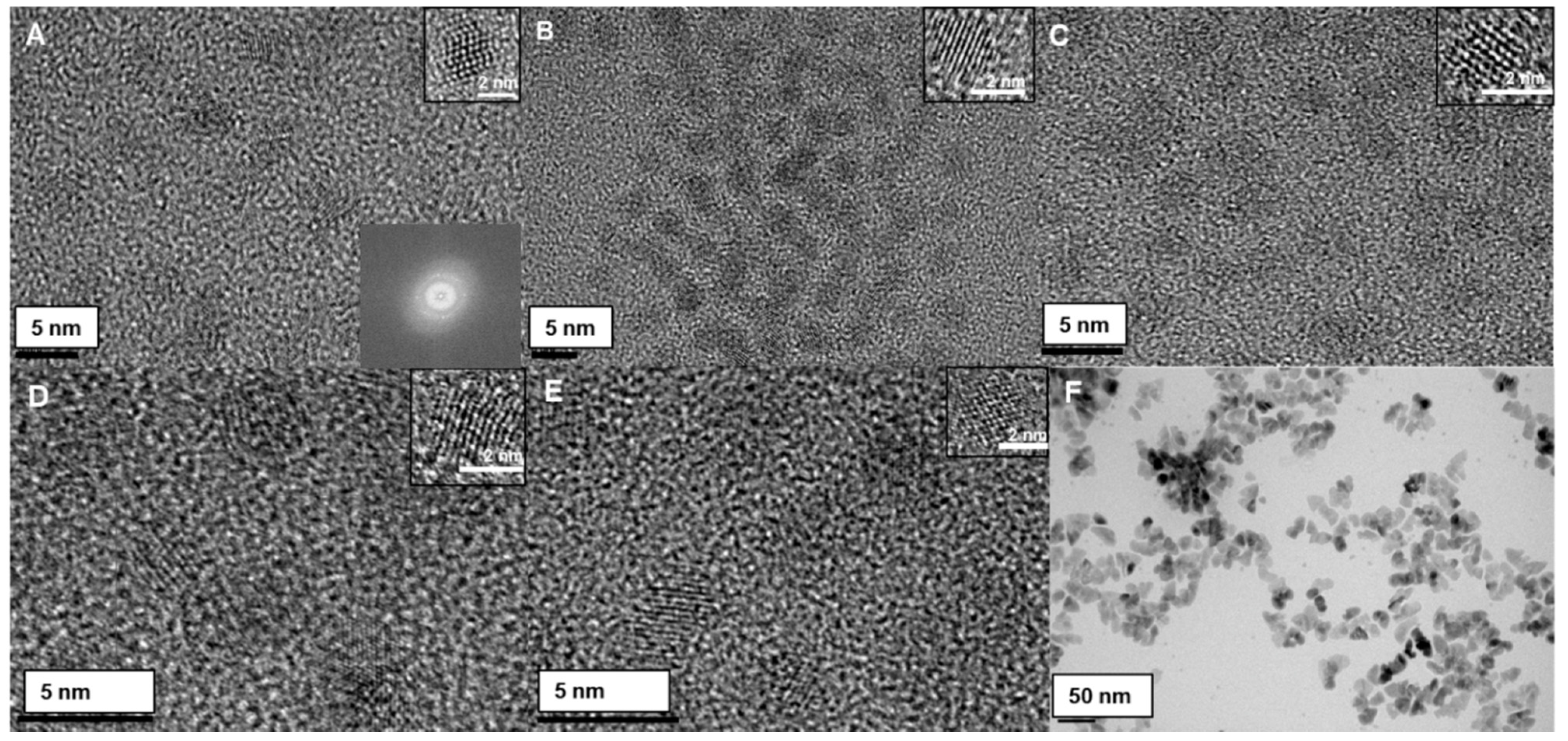
3. Results and Discussions
4. Conclusions
Supplementary Materials
Author Contributions
Funding
Acknowledgments
Conflicts of Interest
References
- Xiao, B.; Hu, R.; Lin, G.; Roy, I.; Yong, K.-T. Enhanced optical transmission and fano resonance through a nanostructured metal thin film. Sci. Rep. 2015, 5, 10393. [Google Scholar] [CrossRef] [Green Version]
- Chen, M.L.; Hu, R.; Lin, G.; Roy, I.; Yong, K.-T. Quantum-dot-conjugated graphene as a probe for simultaneous cancer-targeted fluorescent imaging, tracking, and monitoring drug delivery. Bioconjugate Chem. 2013, 24, 387–397. [Google Scholar] [CrossRef]
- Wang, Y.; Hu, R.; Lin, G.; Roy, I.; Yong, K.-T. Functionalized quantum dots for biosensing and bioimaging and concerns on toxicity. Acs Appl. Mater. Interfaces 2013, 5, 2786–2799. [Google Scholar] [CrossRef]
- Dondapati, H.; Ha, D.; Jenrette, E.; Xiao, B.; Pradhan, A.K. High-performance chemical-bath deposited CdS thin-film transistors with ZrO2 gate dielectric. Appl. Phys. Lett. 2014, 105, 052105. [Google Scholar] [CrossRef] [Green Version]
- Nguyen, T.L.; Margaret, M.; Paul, M. Synthesis of highly crystalline CdSe@ZnO nanocrystals via monolayer-by-monolayer epitaxial shell deposition. Chem. Mater. 2014, 26, 4274–4279. [Google Scholar] [CrossRef]
- Dondapati, H.; Ha, D.; Pradhan, A.K. Enhanced photocurrent in solution processed electronically coupled CdSe nanocrystals thin films. Appl. Phys. Lett. 2013, 103, 121114. [Google Scholar] [CrossRef] [Green Version]
- Alivisatos, A.P. Semiconductor clusters, nanocrystals, and quantum dots. Science 1996, 271, 933. [Google Scholar] [CrossRef] [Green Version]
- Jenrette, E.; Pradhan, S.K.; Rutherford, G.; Flowers, J.; Ha, D.; Pradhan, A.K. Quantum-dot-conjugated graphene oxide as an optical tool for biosensor. Opt. Express 2015, 23, 25017–25027. [Google Scholar] [CrossRef]
- An, L.M.; Chen, X.L.; Han, X.T.; Yi, J.; Liu, C.X.; An, W.Y.; Qu, Y.Q.; Chi, J.G.; Wei, H.; Qi, K.Y. CdSe/ZnO core/shell semiconductor nanocrystals: Synthesis and characterization. Appl. Mech. Mater. 2012, 268, 207–210. [Google Scholar] [CrossRef]
- Chakraborty, T.; Chakraborty, I.; Moulik, S.P.; Ghosh, S. Physicochemical and conformational studies on BSA−Surfactant interaction in aqueous medium. Langmuir 2009, 25, 3062–3074. [Google Scholar] [CrossRef] [PubMed]
- Efremov, E.V.; Freek, A.; Cees, G. Achievements in resonance raman spectroscopy: Review of a technique with a distinct analytical chemistry potential. Anal. Chim. Acta 2008, 606, 119–134. [Google Scholar] [CrossRef]
- Liu, Y.; Liu, Q.; Chen, S.; Cheng, F.; Wang, H.; Peng, W. Surface plasmon resonance biosensor based on smart phone platforms. Sci. Rep. 2015, 5, 12864. [Google Scholar] [CrossRef] [PubMed] [Green Version]
- Wang, Y.; Luo, Z.; Liu, K.; Wang, J.; Duan, Y. In situ targeting TEM8 via immune response and polypeptide recognition by wavelength-modulated surface plasmon resonance biosensor. Sci. Rep. 2016, 6, 20006. [Google Scholar] [CrossRef] [Green Version]
- Reyes-Goddard, J.M.; Hugh, B.; Nicholas, S. Photodiagnosis using raman and surface enhanced raman scattering of bodily fluids. Photodiagnosis Photodyn. Ther. 2005, 2, 223–233. [Google Scholar] [CrossRef]
- Chiu, N.F.; Teng-Yi, H.; Hsin-Chih, L. Graphene oxide-based surface plasmon resonance biosensors. Adv. Graphene Sci. InTech. 2013, 280, 191–216. [Google Scholar]
- Liu, Z.; Guo, Z.; Zhong, H.; Qin, X.; Wan, M.; Yang, B. Graphene oxide based enhanced raman scattering probes for cancer cell imaging. Phys. Chem. Chem. Phys. 2013, 15, 2961–2966. [Google Scholar] [CrossRef]
- He, S.; Liu, K.-K.; Su, S.; Yan, J.; Mao, X.; Wang, D.; He, Y.; Li, L.-J.; Song, S.; Fan, C. Graphene-based high-efficiency surface-enhanced raman scattering-active platform for sensitive and multiplex DNA detection. Anal. Chem. 2012, 84, 4622–4627. [Google Scholar] [CrossRef] [PubMed]
- Yu, W.W.; Qu, L.; Guo, W.; Peng, X. Experimental determination of the extinction coefficient of CdTe, CdSe and CdS Nanocrystals. Chem. Mater. 2004, 16, 560. [Google Scholar] [CrossRef] [Green Version]
- Zeman, E.J.; Schatz, G.C. An accurate electromagnetic theory study of surface enhancement factors for silver, gold, copper, lithium, sodium, aluminum, gallium, indium, zinc, and cadmium. J. Phys. Chem. 1987, 91, 634–643. [Google Scholar] [CrossRef]
- Cong, S.; Yuan, Y.; Chen, Z.; Hou, J.; Yang, M.; Su, Y.; Zhang, Y.; Li, L.; Li, Q.; Geng, F.; et al. Noble metal-comparable SERS enhancement from semiconducting metal oxides by making oxygen vacancies. Nat. Commun. 2015, 6, 7800–7801. [Google Scholar] [CrossRef]
- Quagliano, L.G. Observation of molecules adsorbed on IIIV semiconductor quantum dots by surface enhanced Raman scattering. J. Am. Chem. Soc. 2004, 126, 7393–7398. [Google Scholar] [CrossRef] [PubMed]
- Li, W.; Zamani, R.; Gil, P.R.; Pelaz, B.; Ibanez, M.; Cadavid, D.; Shavel, A.; Alvarez-Puebla, R.A.; Parak, W.J.; Arbiol, J. CuTe nanocrystals: Shape and size control, plasmonic properties, and use as SERS probes and photo thermal agents. J. Am. Chem. Soc. 2013, 135, 7098–7101. [Google Scholar] [CrossRef] [PubMed]
- Jiang, L.; You, T.; Yin, P.; Shang, Y.; Zhang, D.; Guo, L.; Yang, S. Surface enhanced raman scattering spectra of adsorbates on CuO nanospheres: Charge transfer and electromagnetic enhancement. Nanoscale 2013, 5, 2784–2789. [Google Scholar] [CrossRef]
- Musumeci, A.; Gosztola, D.; Schiller, T.; Dimitrijevic, N.M.; Mujica, V.; Martin, D.; Rajh, T. SERS of semiconducting nanoparticles (TiO hybrid composites). J. Am. Chem. Soc. 2009, 131, 6040–6041. [Google Scholar] [CrossRef] [PubMed]
- Qi, D.; Lu, L.; Wang, L.; Zhang, J. Improved SERS sensitivity on plasmon free TiO2 photonic microarray by enhancing light matter coupling. J. Am. Chem. Soc. 2014, 136, 9886–9889. [Google Scholar] [CrossRef]
- Li, L.; Hutter, T.; Finnemore, A.S.; Huang, F.M.; Baumberg, J.J.; Elliott, S.R.; Steiner, U.; Mahajan, S. Metal oxide nanoparticle mediated enhanced raman scattering and its use in direct monitoring of interfacial chemical reactions. Nano Lett. 2012, 12, 4242–4246. [Google Scholar] [CrossRef] [Green Version]
- Roy, D.; Routh, T.; Asaithambi, A.V.; Mandal, S.; Mandal, P.K. Spectral and temporal optical behavior of blue-, green-, orange-, and red-emitting CdSe-based core/gradient alloy shell/shell quantum dots: Ensemble and single-particle investigation results. J. Phys. Chem. C 2016, 120, 3483–3491. [Google Scholar] [CrossRef]
- Andrew, S.; Aaron, M.; Mohs, M.; Nie, S. Tuning the optical and electronic properties of colloidal nanocrystals by lattice strain. Nat. Nanotechnol. 2009, 4, 56–63. [Google Scholar]
- Li, Y. Characterization of Engineered Nanomaterials by Spectroscopic Ellipsometry. Available online: http://www.horiba.com/fileadmin/uploads/Scientific/Documents/TFilm/AN_SE26_Nanomaterials_HD.pdf (accessed on 6 April 2021).
- Villars, P.; Cenzual, K. Landolt-Börnstein-Group III condensed matter. Landolt Börnstein 2012, 1, 43A11. [Google Scholar]
- Landolt, H.; Börnstein, R. Zinc Oxide (ZnO) Refractive Index. Available online: https://0-materials-springer-com.brum.beds.ac.uk/lb/docs/sm_lbs_978-3-540-31359-5_305 (accessed on 6 April 2021).
- Webster, P.J.; Ziebeck, K.R.A. Landolt-Börnstein—Group III condensed matter (Alloys and Compounds of d-Elements with Main Group Elements. Part 2). Landolt Börnstein 1988, 19C. [Google Scholar] [CrossRef]
- Kochuveedu, S.T.; Son, T.; Lee, Y.; Lee, M.; Kim, D.; Kim, D.H. Revolutionizing the FRET-based light emission in core-shell nanostructures via comprehensive activity of surface plasmons. Sci. Rep. 2014, 4, 4735. [Google Scholar] [CrossRef] [Green Version]
- Herne, T.M.; Ahern, A.M.; Garell, R.L. Surface-enhanced raman spectroscopy of peptides: Preferential n-terminal adsorption on colloidal silver. J. Am. Chem. Soc. 1991, 113, 846–854. [Google Scholar] [CrossRef]
- Campion, A.; Kambhampati, P. Surface-enhanced raman scattering. Chem. Soc. Rev. 1998, 27, 241–250. [Google Scholar] [CrossRef]
- Dzhagan, V.M.; Valakh, M.Y.; E Raevskaya, A.; Stroyuk, O.; Kuchmiy, S.Y.; Zahn, D.R. Size effects on raman spectra of small CdSe nanoparticles in polymer films. Nanotechnology 2008, 19, 305707. [Google Scholar] [CrossRef] [PubMed]
- Schumm, M. ZnO-Based Semiconductors Studied by Raman Spectroscopy: Semimagnetic Alloying, Doping and Nanostructures; Suedwestdeutscher Verlag Fuer Hochschulschriften: Saarbrücken, Germany, 2010. [Google Scholar]
- Lautenschlaeger, S.; Eisermann, S.; Meyer, B.K.; Callison, G.; Wagner, M.R.; Hoffmann, A. Nitrogen incorporation in homoepitaxial ZnO CVD epilayers. Phys. Status Solidi (Rrl) Rapid Res. Lett. 2009, 3, 16–18. [Google Scholar] [CrossRef]
- Chen, M.C.; Lord, R.C. Laser-excited Raman spectroscopy of biomolecules. VIII. Conformational study of bovine serum albumin. J. Am. Chem. Soc. 1976, 98, 990–992. [Google Scholar] [CrossRef] [PubMed]
- Chi, Z.; Chen, X.G.; Holtz, J.S.; Asher, S.A. UV resonance raman-selective amide vibrational enhancement: Quantitative methodology for determining protein secondary structure. Biochemistry 1998, 37, 2854–2864. [Google Scholar] [CrossRef] [PubMed]
- Dong, Z.-G.; Liu, H.; Cao, J.-X.; Li, T.; Wang, S.-M.; Zhu, S.-N.; Zhang, X. Enhanced sensing performance by the plasmonic analog of electromagnetically induced transparency in active metamaterials. Appl. Phys. Lett. 2010, 97, 114101. [Google Scholar] [CrossRef] [Green Version]
- Ahmadivand, A.; Gerislioglu, B.; Tomitaka, A.; Manickam, P.; Kaushik, A.; Bhansali, S.; Nair, M.; Pala, N. Extreme sensitive metasensor for targeted biomarkers identification using colloidal nanoparticles-integrated plasmonic unit cells. Biomed. Opt. Express 2018, 9, 373. [Google Scholar] [CrossRef] [PubMed]
- Toma, M.; Tawa, K. Plasmonic coloration of silver nanodome arrays for a smartphone-based plasmonic biosensor. Nanoscale Adv. 2019. [Google Scholar] [CrossRef] [Green Version]


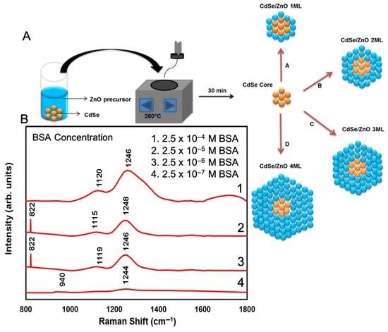
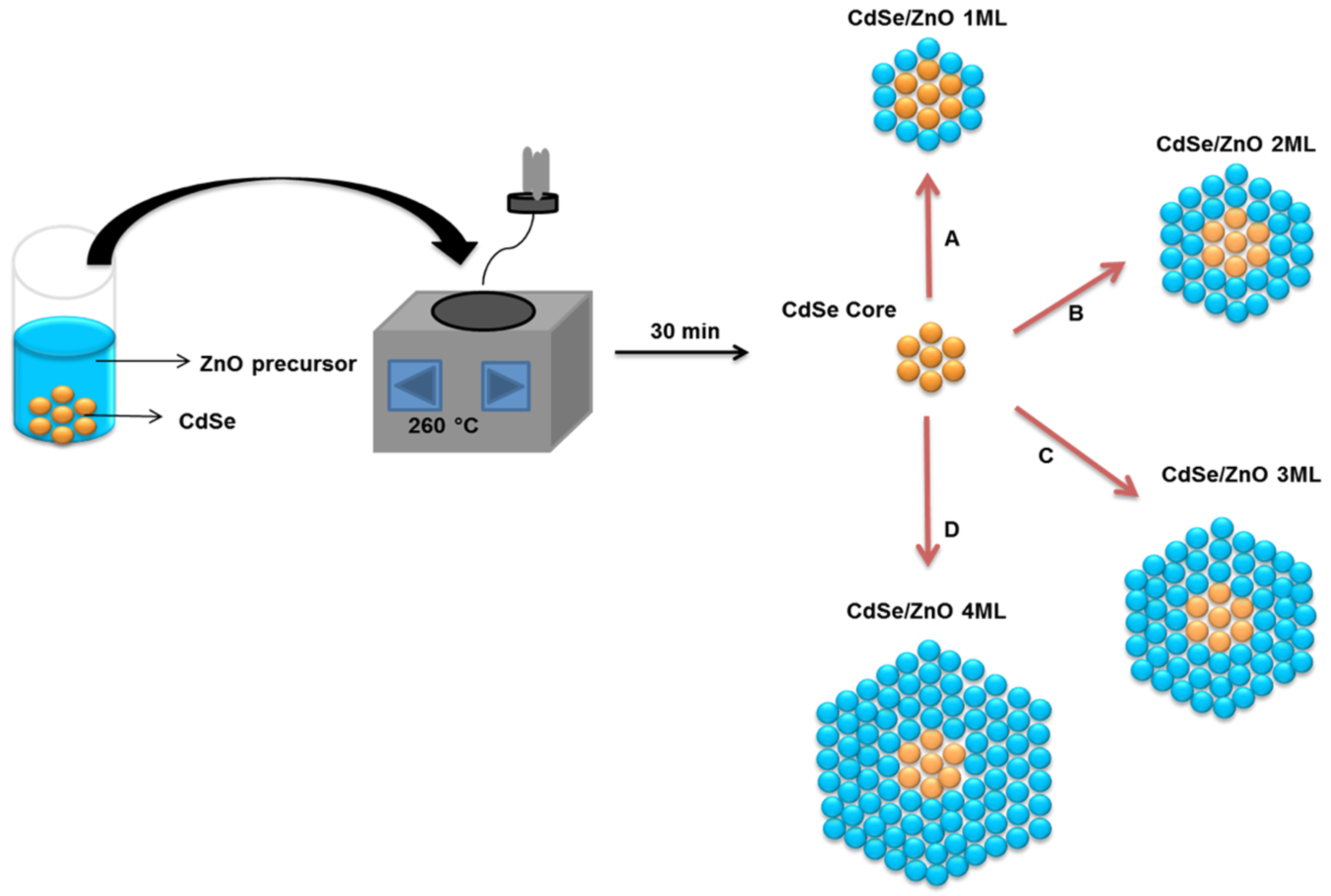
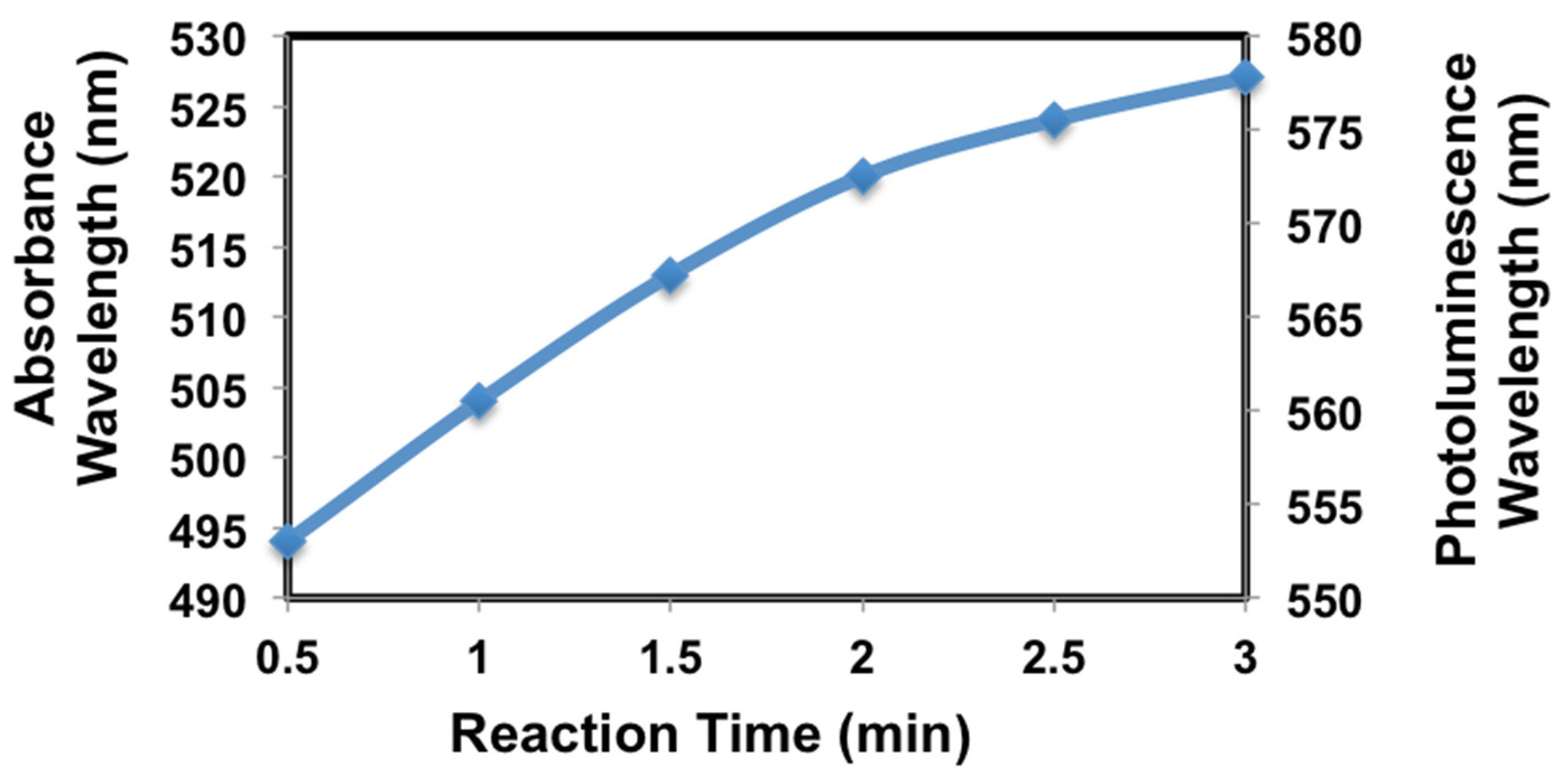
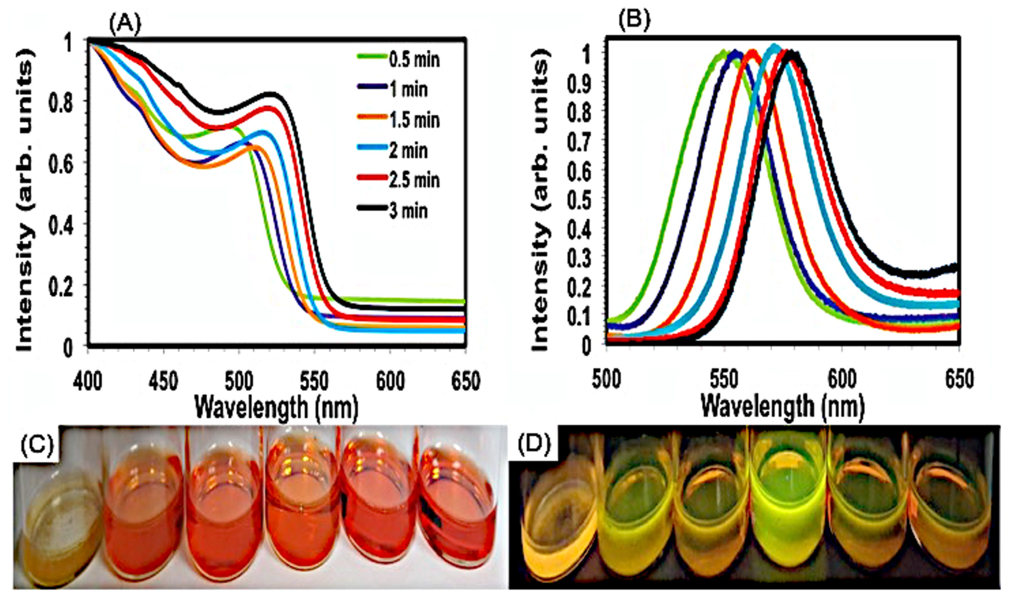
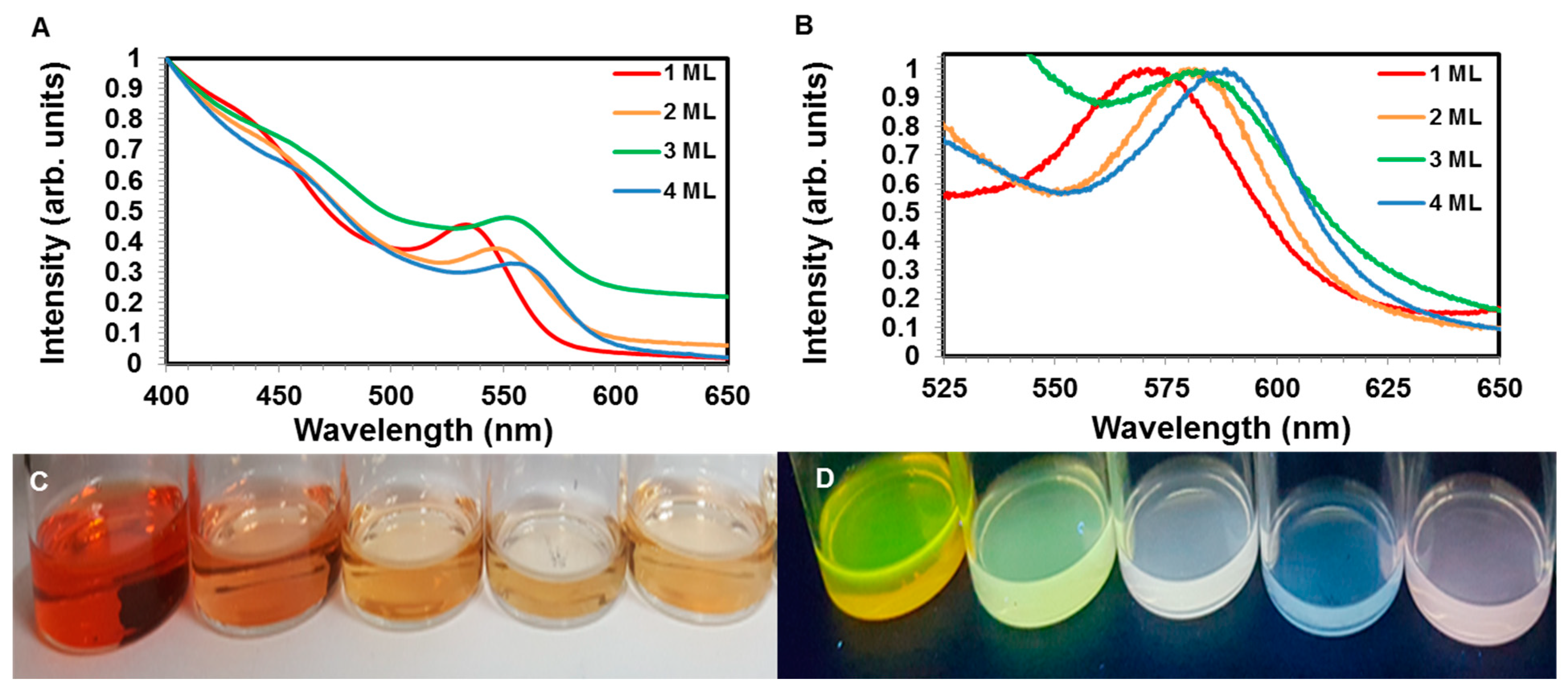
| Number of ZnO Monolayers | Absorbance Wavelength (nm) | Photoluminescence Wavelength (nm) | Average Particle Size (nm) |
|---|---|---|---|
| 0 | 520 | 571 | 2.57 |
| 1 | 537 | 572 | 2.80 |
| 2 | 548 | 581 | 3.00 |
| 3 | 554 | 583 | 3.12 |
| 4 | 561 | 589 | 3.29 |
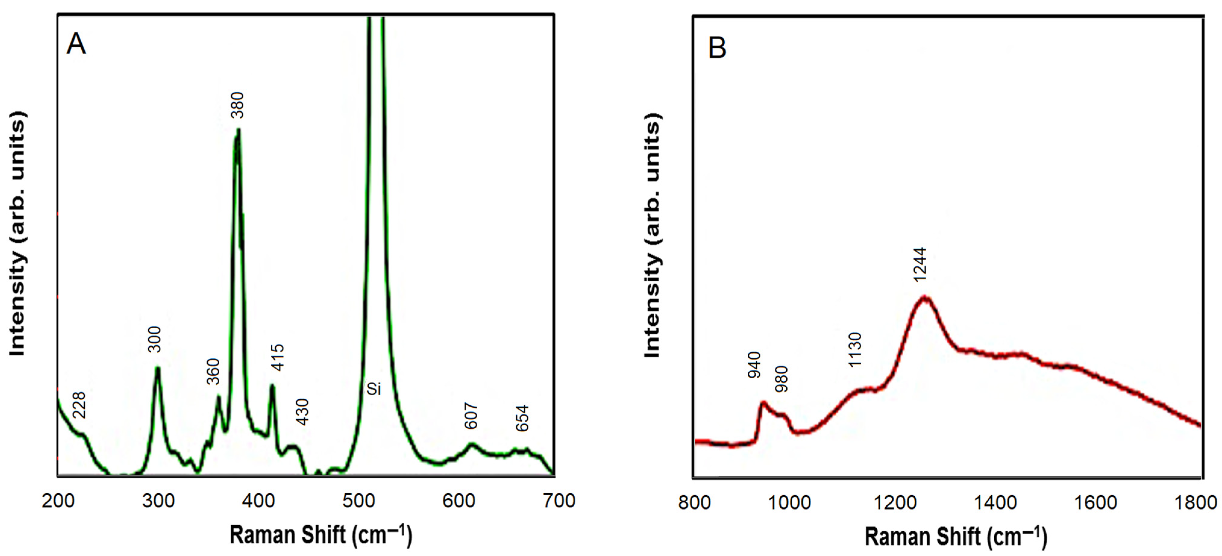
| Number of Raman Modes | CdSe Modes (cm−1) [29,30,31,32,33,34,35,36] | Peaks Observed from CdSe-ZnO (cm−1) | ZnO Modes (cm−1) [37,38] | Peaks Observed from CdSe-ZnO (cm−1) |
|---|---|---|---|---|
| 1 | 210 | 228 | 284 | 300 |
| 2 | 228 | 430 | 332 | 360 |
| 3 | 425 | 607 | 378 | 380 |
| 4 | 607 | - | 410 | 415 |
| 5 | - | - | 438 | 430 |
| 6 | - | - | 590 | - |
| 7 | - | - | 618 | - |
| 8 | - | - | 657 | 654 |
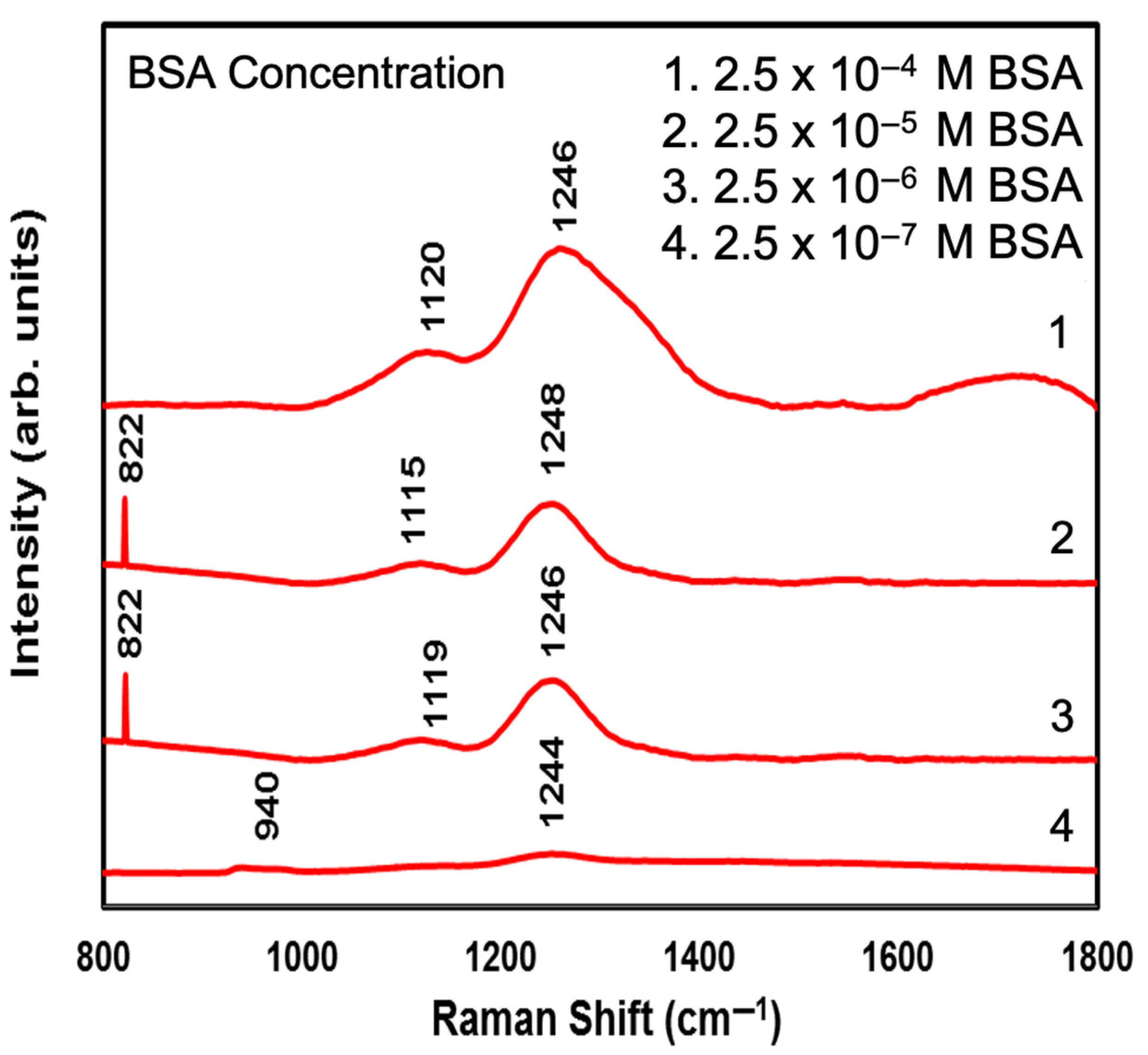
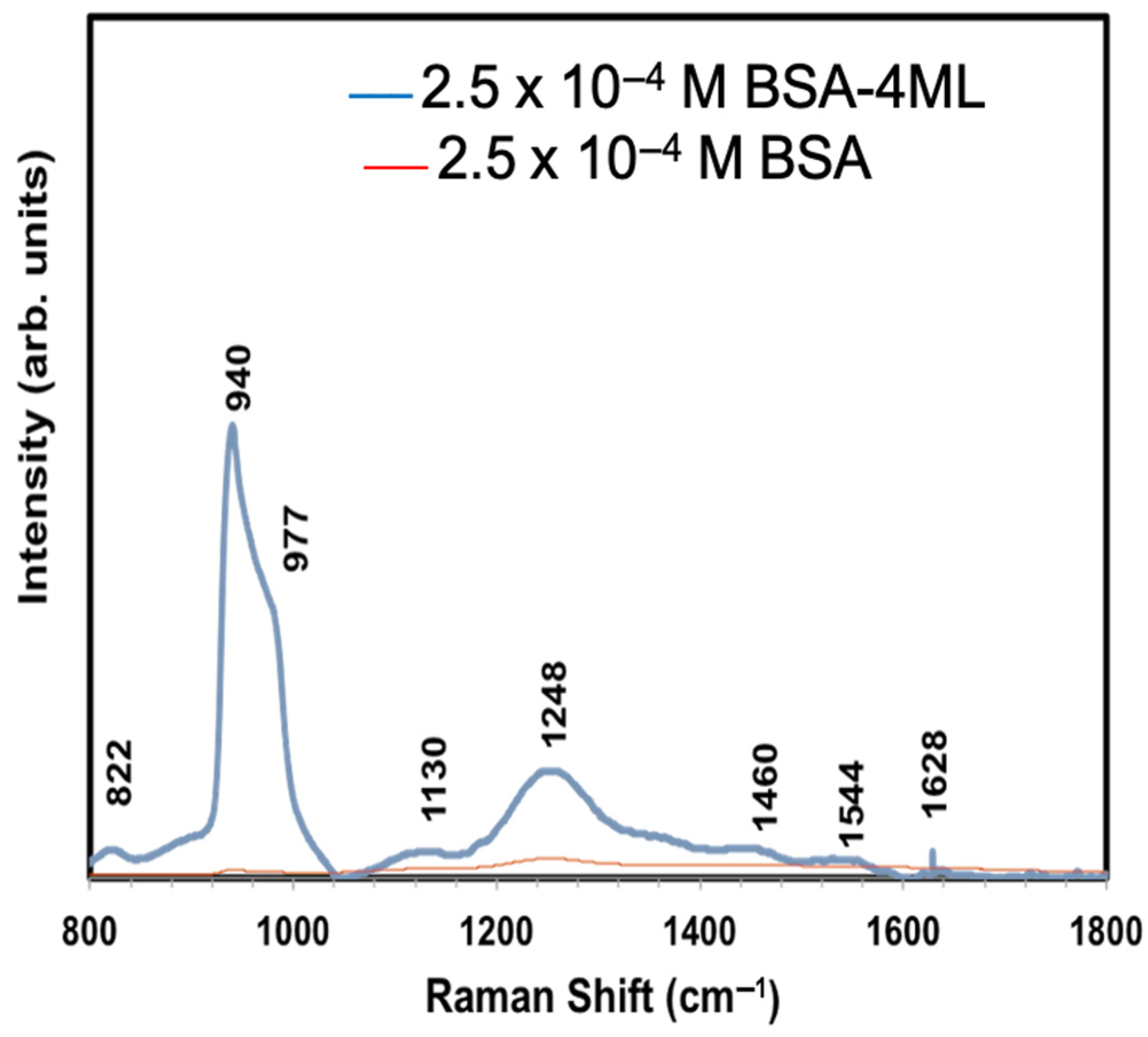
| Number of Raman Modes | 2.5 × 10⁻⁴ M BSA on a Si Substrate (cm−1) | 2.5 × 10⁻⁴ M BSA on a CdSe-ZnO-4 ML Coated Si Substrate (cm−1) | Band Assignment Peaks of BSA (cm−1) [39,40] |
|---|---|---|---|
| 1 | 940 | 822 | 822 |
| 2 | 980 | 940 | 940 |
| 3 | 1130 | 977 | 979 |
| 4 | 1244 | 1130 | 1127 |
| 5 | - | 1248 | 1254 |
| 6 | - | - | 1359 |
| 7 | - | 1460 | 1458 |
| 8 | - | 1544 | 1530 |
| 9 | - | 1628 | 1633 |
Publisher’s Note: MDPI stays neutral with regard to jurisdictional claims in published maps and institutional affiliations. |
© 2021 by the authors. Licensee MDPI, Basel, Switzerland. This article is an open access article distributed under the terms and conditions of the Creative Commons Attribution (CC BY) license (https://creativecommons.org/licenses/by/4.0/).
Share and Cite
Jenrette, E.A.; Farrell, M.J.; Flowers, J.A.; Pradhan, A.K. CdSe-ZnO Core–Shell Quantum Dots for Protein Detection: A Potential Sensing Platform. Nanomanufacturing 2021, 1, 3-13. https://0-doi-org.brum.beds.ac.uk/10.3390/nanomanufacturing1010002
Jenrette EA, Farrell MJ, Flowers JA, Pradhan AK. CdSe-ZnO Core–Shell Quantum Dots for Protein Detection: A Potential Sensing Platform. Nanomanufacturing. 2021; 1(1):3-13. https://0-doi-org.brum.beds.ac.uk/10.3390/nanomanufacturing1010002
Chicago/Turabian StyleJenrette, Erin A., Monique J. Farrell, Jasmin A. Flowers, and Aswini K. Pradhan. 2021. "CdSe-ZnO Core–Shell Quantum Dots for Protein Detection: A Potential Sensing Platform" Nanomanufacturing 1, no. 1: 3-13. https://0-doi-org.brum.beds.ac.uk/10.3390/nanomanufacturing1010002