
Two-Dimensional Nanograting Fabrication by Multistep Nanoimprint Lithography and Ion Beam Etching


1
Faculty of Engineering, Kiel University, Kaiserstraße 2, 24143 Kiel, Germany
2
Department Optics for Solar Energy, Helmholtz-Zentrum Berlin, Albert-Einstein-Str. 16, 12489 Berlin, Germany
*
Author to whom correspondence should be addressed.
Nanomanufacturing 2021, 1(1), 39-48; https://0-doi-org.brum.beds.ac.uk/10.3390/nanomanufacturing1010004
Submission received: 1 April 2021
/
Revised: 28 April 2021
/
Accepted: 4 May 2021
/
Published: 19 May 2021
Abstract
:The application of nanopatterned electrode materials is a promising method to improve the performance of thin-film optoelectronic devices such as organic light-emitting diodes (OLEDs) and organic photovoltaics. Light coupling to active layers is enhanced by employing nanopatterns specifically tailored to the device structure. A range of different nanopatterns is typically evaluated during the development process. Fabrication of each of these nanopatterns using electron-beam lithography is time- and cost-intensive, particularly for larger-scale devices, due to the serial nature of electron beam writing. Here, we present a method to generate nanopatterns of varying depth with different nanostructure designs from a single one-dimensional grating template structure with fixed grating depth. We employ multiple subsequent steps of UV nanoimprint lithography, curing, and ion beam etching to fabricate greyscale two-dimensional nanopatterns. In this work, we present variable greyscale nanopatterning of the widely used electrode material indium tin oxide. We demonstrate the fabrication of periodic pillar-like nanostructures with different period lengths and heights in the two grating directions. The patterned films can be used either for immediate device fabrication or pattern reproduction by conventional nanoimprint lithography. Pattern reproduction is particularly interesting for the large-scale, cost-efficient fabrication of flexible optoelectronic devices.
1. Introduction
The performance of thin-film optoelectronic devices, such as organic and perovskite light-emitting diodes (OLEDs and PeLEDs) and organic photovoltaics (OPV), has been increasing steadily over the last decades [1,2,3,4]. However, their efficiencies are still limited by losses inherent to the device architecture. In a default device stack, more than 80% of the light cannot be utilized because of coupling to substrate modes, waveguided modes in the active layers or plasmonic modes at metal interfaces [5,6]. Various methods to access the light trapped in these modes such as the application of high-index substrate materials or the addition of one or multiple extraction lenses have been proposed [7,8]. Another promising approach is the introduction of a periodic or aperiodic nanopattern to the interfaces in the layer stack [9,10,11,12,13,14,15]. The nanostructure reduces total internal reflection and enables the outcoupling of quasi-guided modes [16,17]. Additionally, charge carrier injection may benefit from local field enhancement effects at nanopatterned electrodes [18,19]. To achieve a significant increase in coupling efficiency, the geometrical dimensions of the employed nanopattern must be adjusted to the particular device design. Suitable parameters can be determined via simulation of the layer stack [20]. In an LED, the maximum increase in outcoupling efficiency should match the emission maximum, whereas the maximum increase in coupling to the active layer in a solar cell should coincide with the absorption peak. Aside from enhancing the overall efficiency, periodic nanopatterns also allow for directional coupling of selective wavelengths [21,22], and may facilitate nanoparticle alignment during device fabrication [23,24].
Recently, flexible organic optoelectronics have gained increased attention as they enable novel applications such as bendable or foldable displays, wearable devices or printable sensing systems [25,26,27,28]. The integration of nanopatterns in flexible devices may increase performance and add new functionality [29,30,31]. Mechanical deformation of nanogratings results in shifting of resonance characteristics, making such devices promising candidates for strain sensors or tunable light sources [32,33]. Consequently, the utilized nanomanufacturing process must be suitable for the fabrication of flexible nanogratings on large device areas (cm² range) which are required for most of these applications.
In order to comply with specific requirements for different device architectures, a process to generate nanopatterned electrode films for device development must also enable the creation of different shapes and pattern designs with adjustable structural heights. This effectively requires a highly controllable greyscale patterning method. Even though multiple greyscale electron beam lithography (EBL) techniques have been developed [34,35,36,37], they are usually complex, time-consuming and not suitable for large-scale patterning. Other techniques such as interference lithography (IL) or extreme ultraviolet lithography (EUVL) are available for large area patterning, but at the same time require high equipment investment costs and oftentimes multiple exposure steps to obtain two-dimensional greyscale patterns [38,39]. On the other hand, nanoimprint lithography (NIL) is a low-cost process allowing for high-throughput reproduction of multiscale patterns [40,41,42,43]. However, the obtainable nanopatterns are essentially restricted to the geometrical shape and dimensions of the imprint template [44,45].
In this work, we present a manufacturing method to introduce nanopatterns of variable shapes and heights into a transparent conductive indium tin oxide (ITO) film on a glass substrate. As ITO is the most commonly used electrode material for thin film optoelectronics, the resulting samples can be directly used for device fabrication. Additionally, they may also be utilized as imprint templates for simple reproduction of the generated pattern by NIL. We are able to create arbitrary two-dimensional greyscale patterns by performing multiple successive nanoimprint steps employing the same or different template patterns in each step. Our method allows for the utilization of master templates fabricated by other techniques such as IL or EUVL for simple and cost-efficient variation of feature heights and generation of composite nanopatterns. In contrast to other works applying multiple nanoimprint steps to achieve multi-dimensional patterns [46], we cure and etch the imprint resist after each imprint step. In doing so, we are able to maintain structural conformity to the desired pattern and to obtain greyscale features.
2. Materials and Methods
The different stages of the nanopatterning process are depicted in Figure 1. One or more initial master templates patterned by electron beam lithography, laser interference lithography, or other techniques are required as a basis for the resulting nanopattern. We used commercially available glass templates (25 × 25 mm², AMO GmbH, Aachen, Germany) patterned by conventional laser interference lithography which hold periodic one-dimensional nanogratings with period lengths ranging from 400 to 600 nm and a grating height of 140 nm. From the master templates, we reproduced negative imprint templates from polydimethylsiloxane (PDMS), which we applied for up to three successive imprints. Subsequently, we employed a standard UV nanoimprint process described previously to impress the positive pattern into an imprint resist layer [47]. Patterning was performed on ITO-coated glass substrates (25 × 25 mm², specified ITO layer thickness 140 nm ± 20 nm, Lumtec, New Taipei City, Taiwan) utilizing the UV-curable imprint resist Amonil MMS4 (AMO GmbH, Aachen, Germany), which is an organic–inorganic composite containing zirconium alkoxides. The imprint resist was spin-coated onto the substrate surface and the imprint template was manually applied before UV curing. Since the grating height of the master template is generally lower than the total imprint resist layer thickness, a residual layer of imprint resist remains between the nanopattern and the ITO coating, which is removed during the pattern transfer. After reproduction of the one-dimensional pattern in the resist, we transferred the structure into the ITO layer by ion beam etching (IBE) using an IBE system PC3000 (Oxford Instruments, Abingdon, UK). We employed a purely physical ion etching technique using only argon (Ar) plasma as the etchant in order to achieve a highly anisotropic etching. Choosing an RF power of 500 W and a beam current of 350 mA at a gas pressure of 8 torr allowed for a precisely controllable etching process while maintaining a reasonable processing time, resulting in an ITO etching rate of 22.4 nm/min. A detailed etching rate analysis including the etching rate for the imprint resist is provided in Section 3 of this work. Following the pattern transfer, we removed any residues of the imprint resist with tetramethylammonium hydroxide using a commercial photoresist stripper (TechniStrip P1316, MicroChemicals, Ulm, Germany). By repeating the imprint and etching process, rotating the imprint template by an angle for each imprint step, we obtained two-dimensional greyscale patterns on an area of around 4 cm² in the ITO. A digital photograph of an ITO layer patterned with the method described above is depicted in Figure 2.
3. Results
The maximum structural depth for the first etching step is determined by the height of the imprint template and the etching rate ratio between the imprint resist and the ITO layer. To perform an etching rate analysis at the chosen etching parameters, we prepared several planar samples with and without the imprint resist. We etched partially masked samples for different times before measuring the resulting height difference with a profilometer. The measurements shown in Figure 3 indicate constant etching rates over the entire process duration, corresponding to an etching rate ratio of 1.2. Despite the low selectivity of the etching process (which is expected for a purely physical etching), it is suitable to transfer the grating pattern into the underlying ITO layer. However, as the ITO etching rate is lower than the etching rate of the imprint resist, the maximum structural depth possible is only 116 nm (83% of the height of the imprint template).
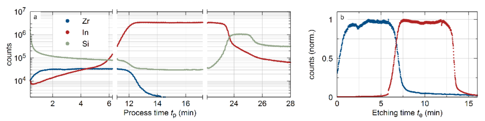
The actual etching time for each sample was chosen according to the desired etching depth assuming the etching rates presented before. In order to account for potential thickness variations of the imprint resist during deposition, the etching process was additionally tracked in situ by time-of-flight secondary ion mass spectrometry (TOF-SIMS), as shown in Figure 4. Since the imprint resist contains zirconium (Zr), one can qualitatively track the presence of resist on the sample surface by monitoring the Zr content in the secondary ion gas mixture. While etching a planar sample onto which an unpatterned imprint template had been applied, the Zr count decreases sharply after approximately 7 min, indicating complete removal of the imprint resist and exposure of the ITO layer underneath. At the same time, the indium (In) count rises abruptly, corresponding to the beginning of the ITO etching. The slight increase in the In count during the first minutes of the etching process, which is visible in the logarithmic representation (Figure 4a), is attributed to increasing lateral etching of the ITO layer at the sample edges. However, as the absolute contribution to the In count is low (as seen in the normalized representation in Figure 4b), we do not expect monitoring of the ITO etching to be affected. After a total etching time of 15 min, the In count declines again indicating that the ITO layer is entirely removed. The sudden increase of the Si count at this point can be attributed to the etching of a 20 nm thick SiO2 passivation layer underneath the ITO coating. Considering the etching durations for planar layers of the imprint resist (approx. 200 nm) and the ITO coating (140 nm ± 20 nm) indicated in Figure 4b, an etching rate ratio of 1.45 ± 0.2 is estimated. The discrepancy between this value and the ratio calculated from the etching rate analysis may be mainly attributed to uncertainties in total layer thickness of the imprint resist layer as well as the ITO coating. Furthermore, the thickness of the residual imprint resist remaining between the pattern and the ITO surface may be different in nanopatterned samples due to manual application of the imprint pressure. This emphasizes the importance of the in situ tracking by mass spectrometry as it allows precise detection of the starting point of the ITO etching and calculation of the required etching time using the etching rates presented in Figure 3 irrespective of the actual residual imprint resist layer thickness. Since the reproducibility of the grating patterns by nanoimprint lithography is high, we do not expect significant variations in the pattern periodicity. However, the etching depth homogeneity is strongly influenced by thickness variations of the residual imprint resist layer across the sample surface. Discrepancies in imprint resist thickness at different spots on the surface lead to temporal deviations in the onset point of the ITO etching, reducing the slope of the In count in Figure 4b. We determined the rise time for the In signal–defined as the time required for the signal to rise from 10% to 90% of its maximum value–to be approximately 68 s. Taking into account the aforementioned etching rates, the maximum thickness difference after the imprint process is estimated to be around 31 nm. This value is considerable compared to the total layer thickness of 200 nm and the original grating height of 140 nm, potentially leading to etching depth variations of up to 25 nm across the sample surface. It should be noted, though, that homogeneity of the residual imprint resist layer is difficult to achieve with the manual imprint process we employed in this work and may vary from sample to sample. We expect variations of the residual imprint resist layer thickness to be much lower if an optimized and automated imprint process is employed, which would significantly improve etching depth homogeneity across the sample surface.
By repeating the imprint and etching process, rotating the imprint template by an angle for each imprint step, we obtain two-dimensional greyscale patterns in the ITO. In order to determine the etching time for subsequent patterning steps, the additional residual imprint resist layer due to the existing nanograting must be taken into account. During coating, the imprint resist fills the voids of the underlying pattern while partly preserving the structure through the layer. However, application of the imprint template forces a new pattern onto the surface, causing differences in resist thickness, which result from both the existing pattern underneath the resist and the newly imprinted grating. For the calculation of the required etching time, the additional residual imprint resist layer thickness (which is equal to the grating height of the existing pattern) must be considered. As the etching rate of the imprint resist is higher than the etching rate of the ITO, this effect finally leads to flattening of the existing pattern during successive etching steps. While the flattening may be utilized to easily obtain different step heights, one can also diminish it by choosing the etching time accordingly. The ability to attain multiple step heights in the final nanopattern allows for the fabrication of greyscale features with controllable pattern height for each of the grating directions. Although the etch selectivity is low, flattening of underlying patterns during the transfer of additional patterns was observed, indicating that the final step heights cannot be chosen for each etching step independently. Instead, etching times have to be calculated carefully, taking into account all etching steps performed during nanopattern fabrication as well as different etching rates for the imprint resist and ITO coating, in order to obtain the desired feature shape. The final shape of the resulting nanopattern is determined by the number of the performed imprint and etching steps as well as the angles in which the imprint templates are applied. One can simply obtain square pillar patterns by using the same imprint template, holding a 1D grating structure and rotating it by 90° for the second imprint step. Other designs (such as rectangular or rhomboid-shaped pillars) can be fabricated by using multiple 1D templates with different period lengths or applying the PDMS templates at different angles. Examples of various different greyscale pattern designs fabricated with our method are presented in Figure 5. The generation of more complex patterns, such as isosceles triangles, requires more than two imprint steps and, therefore, exact alignment of the imprint templates. For this work, all alignment was done manually, hence preventing the fabrication of those patterns. However, as alignment precision below 100 nm has been shown to be feasible for NIL [48], we expect our method to be suitable for the generation of arbitrary periodic and aperiodic patterns from appropriate master templates.
This nanofabrication approach may be used, in particular, to realize new master templates for pattern duplication via standard nanoimprint lithography techniques. In order to show the applicability of our method to this workflow, we covered the etched ITO gratings with an anti-sticking layer (BGL-GZ-83) and used them as a mold for PDMS imprint templates. With these PDMS stamps, we performed a standard UV nanoimprint lithography process yielding a nanopatterned layer of imprint resist on a glass substrate, which was coated with a thin silver layer for SEM (Scanning electron microscopy, Helios NanoLab 600, FEI, Hillsboro, OR, USA) imaging. A comparison of the employed ITO templates and the resulting imprinted nanopatterns is presented in Figure 6. Both the one-dimensional grating pattern (Figure 6a) and the two-dimensional pillar pattern (Figure 6c) show very good conformity to the period length and grating depth of the templates (Figure 6b,d), confirming that the etched ITO samples can indeed be used as master templates for pattern replication. The imprinted samples exhibit higher surface roughness and less distinct pattern features than the templates. We attribute this mainly to the silver coating on top of the resist and not to be a result of the imprint process itself. This is due to the fact that silver may form rough films especially when deposited at the low rates necessary for the fabrication of very thin layers [49], whereas we did not observe roughening of the pattern during any other imprints using the same template material and imprint resist.
4. Discussion
We have demonstrated a method to generate variable two-dimensional greyscale nanopatterns in indium tin oxide using only a one-dimensional nanoimprint master template. The patterning process consists of multiple successive steps of nanoimprint lithography and ion beam etching. Greyscale features are obtainable because we cure and etch the imprint resist after each imprint step, allowing individual etch durations for each etching step. Additionally, we employed secondary ion mass spectrometry to track the etching progress and precisely control the etching depth, yielding two-dimensional patterns with variable feature height. Although the fabricated nanopatterns were not integrated into optoelectronic devices during this work, we expect device performance to be similar to devices using nanopatterned ITO electrodes fabricated by other techniques [14,19]. Since the generation of complex multi-dimensional patterns from one-dimensional master templates requires multiple imprint and etching steps, exact reproducibility between different samples may be difficult to achieve. We, therefore, envision the main application of our method to be the fabrication of new master template patterns. Subsequently, one may utilize these master templates for pattern duplication via highly reproducible standard nanoimprint lithography techniques. We demonstrated this workflow by reproducing multiple etched patterns using a standard UV nanoimprint lithography technique. Generating new variable master templates by nanoimprint lithography and ion beam etching using only one or few existing templates is particularly beneficial in cases where greyscale EBL is not feasible due to the fabrication-time constraints with large substrate sizes. The advantage of our technique is that all processing steps are performed in parallel for the complete surface with a fixed process time independent of substrate size. Our technique may be combined with laser-interference lithography approaches for generating different nanostructure depths and composite nanostructures without renewed laser exposure. The process described in this work exemplifies this procedure by utilizing only three master templates fabricated externally by laser interference lithography to produce a variety of two-dimensional nanopatterns with different shapes and feature sizes. This approach allows for simple variations of structural parameters in cases where repeated fabrication of master templates is not viable due to time or cost constraints.
Author Contributions
Conceptualization, J.B. and M.G.; validation, J.B.; investigation, J.B., D.Y. and M.K.; resources, M.K.; writing—original draft preparation, J.B.; writing—review and editing, J.B., D.Y., M.K. and M.G.; visualization, J.B.; supervision, M.G.; project administration, M.G.; funding acquisition, M.G. All authors have read and agreed to the published version of the manuscript.
Funding
This research was funded by Interreg (Project Rollflex, 1_11.12.2014).
Data Availability Statement
Data are contained within the article.
Conflicts of Interest
The authors declare no conflict of interest.
References
- Tang, C.W.; VanSlyke, S.A. Organic electroluminescent diodes. Appl. Phys. Lett. 1987, 51, 913–915. [Google Scholar] [CrossRef]
- Reineke, S.; Lindner, F.; Schwartz, G.; Seidler, N.; Walzer, K.; Lüssem, B.; Leo, K. White organic light-emitting diodes with fluorescent tube efficiency. Nature 2009, 459, 234–238. [Google Scholar] [CrossRef]
- Shaheen, S.E.; Brabec, C.J.; Sariciftci, N.S.; Padinger, F.; Fromherz, T.; Hummelen, J.C. 2.5% efficient organic plastic solar cells. Appl. Phys. Lett. 2001, 78, 841–843. [Google Scholar] [CrossRef] [Green Version]
- Li, S.; Ye, L.; Zhao, W.; Yan, H.; Yang, B.; Liu, D.; Li, W.; Ade, H.; Hou, J. A Wide Band Gap Polymer with a Deep Highest Occupied Molecular Orbital Level Enables 14.2% Efficiency in Polymer Solar Cells. J. Am. Chem. Soc. 2018, 140, 7159–7167. [Google Scholar] [CrossRef] [PubMed]
- Meerheim, R.; Furno, M.; Hofmann, S.; Lüssem, B.; Leo, K. Quantification of energy loss mechanisms in organic light-emitting diodes. Appl. Phys. Lett. 2010, 97, 253305. [Google Scholar] [CrossRef]
- Furno, M.; Rosenow, T.C.; Gather, M.C.; Lüssem, B.; Leo, K. Analysis of the external and internal quantum efficiency of multi-emitter, white organic light emitting diodes. Appl. Phys. Lett. 2012, 101, 143304. [Google Scholar] [CrossRef]
- Mladenovski, S.; Neyts, K.; Pavicic, D.; Werner, A.; Rothe, C. Exceptionally efficient organic light emitting devices using high refractive index substrates. Opt. Express 2009, 17, 7562–7570. [Google Scholar] [CrossRef] [PubMed] [Green Version]
- Möller, S.; Forrest, S.R. Improved light out-coupling in organic light emitting diodes employing ordered microlens arrays. J. Appl. Phys. 2002, 91, 3324–3327. [Google Scholar] [CrossRef] [Green Version]
- Li, Y.; Kovačič, M.; Westphalen, J.; Oswald, S.; Ma, Z.; Hänisch, C.; Will, P.-A.; Jiang, L.; Junghaehnel, M.; Scholz, R.; et al. Tailor-made nanostructures bridging chaos and order for highly efficient white organic light-emitting diodes. Nat. Commun. 2019, 10, 2972. [Google Scholar] [CrossRef]
- Do, Y.R.; Kim, Y.-C.; Song, Y.-W.; Lee, Y.-H. Enhanced light extraction efficiency from organic light emitting diodes by insertion of a two-dimensional photonic crystal structure. J. Appl. Phys. 2004, 96, 7629–7636. [Google Scholar] [CrossRef] [Green Version]
- Jeon, S.; Kang, J.-W.; Park, H.-D.; Kim, J.-J.; Youn, J.R.; Shim, J.; Jeong, J.; Choi, D.-G.; Kim, K.-D.; Altun, A.O.; et al. Ultraviolet nanoimprinted polymer nanostructure for organic light emitting diode application. Appl. Phys. Lett. 2008, 92, 223307. [Google Scholar] [CrossRef]
- Ishihara, K.; Fujita, M.; Matsubara, I.; Asano, T.; Noda, S.; Ohata, H.; Hirasawa, A.; Nakada, H.; Shimoji, N. Organic light-emitting diodes with photonic crystals on glass substrate fabricated by nanoimprint lithography. Appl. Phys. Lett. 2007, 90, 111114. [Google Scholar] [CrossRef]
- Jiang, W.; Liu, H.; Yin, L.; Ding, Y. Fabrication of well-arrayed plasmonic mesoporous TiO2/Ag films for dye-sensitized solar cells by multiple-step nanoimprint lithography. J. Mater. Chem. A 2013, 1, 6433–6440. [Google Scholar] [CrossRef]
- Geyer, U.; Hauss, J.; Riedel, B.; Gleiss, S.; Lemmer, U.; Gerken, M. Large-scale patterning of indium tin oxide electrodes for guided mode extraction from organic light-emitting diodes. J. Appl. Phys. 2008, 104, 93111. [Google Scholar] [CrossRef]
- Riedel, B.; Hauss, J.; Geyer, U.; Guetlein, J.; Lemmer, U.; Gerken, M. Enhancing outcoupling efficiency of indium-tin-oxide-free organic light-emitting diodes via nanostructured high index layers. Appl. Phys. Lett. 2010, 96, 243302. [Google Scholar] [CrossRef]
- Choi, J.; Koh, T.-W.; Lee, S.; Yoo, S. Enhanced light extraction in organic light-emitting devices: Using conductive low-index layers and micropatterned indium tin oxide electrodes with optimal taper angle. Appl. Phys. Lett. 2012, 100, 233303. [Google Scholar] [CrossRef] [Green Version]
- Kluge, C.; Rädler, M.; Pradana, A.; Bremer, M.; Jakobs, P.-J.; Barié, N.; Guttmann, M.; Gerken, M. Extraction of guided modes from organic emission layers by compound binary gratings. Opt. Lett. 2012, 37, 2646–2648. [Google Scholar] [CrossRef]
- Fujita, M.; Ueno, T.; Ishihara, K.; Asano, T.; Noda, S.; Ohata, H.; Tsuji, T.; Nakada, H.; Shimoji, N. Reduction of operating voltage in organic light-emitting diode by corrugated photonic crystal structure. Appl. Phys. Lett. 2004, 85, 5769–5771. [Google Scholar] [CrossRef] [Green Version]
- Fujita, M.; Ishihara, K.; Ueno, T.; Asano, T.; Noda, S.; Ohata, H.; Tsuji, T.; Nakada, H.; Shimoji, N. Optical and Electrical Characteristics of Organic Light-Emitting Diodes with Two-Dimensional Photonic Crystals in Organic/Electrode Layers. Jpn. J. Appl. Phys. 2005, 44, 3669–3677. [Google Scholar] [CrossRef]
- Lüder, H.; Gerken, M. FDTD modelling of nanostructured OLEDs: Analysis of simulation parameters for accurate radiation patterns. Opt. Quantum Electron. 2019, 51, 139. [Google Scholar] [CrossRef] [Green Version]
- Schwab, T.; Fuchs, C.; Scholz, R.; Zakhidov, A.; Leo, K.; Gather, M.C. Coherent mode coupling in highly efficient top-emitting OLEDs on periodically corrugated substrates. Opt. Express 2014, 22, 7524–7537. [Google Scholar] [CrossRef] [PubMed] [Green Version]
- Zhang, S.; Turnbull, G.A.; Samuel, I.D.W. Highly Directional Emission and Beam Steering from Organic Light-Emitting Diodes with a Substrate Diffractive Optical Element. Adv. Opt. Mater. 2014, 2, 343–347. [Google Scholar] [CrossRef] [Green Version]
- Polywka, A.; Tückmantel, C.; Görrn, P. Light controlled assembly of silver nanoparticles. Sci. Rep. 2017, 7, 45144. [Google Scholar] [CrossRef] [PubMed] [Green Version]
- Iwahashi, T.; Yang, R.; Okabe, N.; Sakurai, J.; Lin, J.; Matsunaga, D. Nanoimprint-assisted fabrication of high haze metal mesh electrode for solar cells. Appl. Phys. Lett. 2014, 105, 223901. [Google Scholar] [CrossRef]
- Keum, C.; Murawski, C.; Archer, E.; Kwon, S.; Mischok, A.; Gather, M.C. A substrateless, flexible, and water-resistant organic light-emitting diode. Nat. Commun. 2020, 11, 1–9. [Google Scholar] [CrossRef] [PubMed]
- Yokota, T.; Zalar, P.; Kaltenbrunner, M.; Jinno, H.; Matsuhisa, N.; Kitanosako, H.; Tachibana, Y.; Yukita, W.; Koizumi, M.; Someya, T. Ultraflexible organic photonic skin. Sci. Adv. 2016, 2, e1501856. [Google Scholar] [CrossRef] [Green Version]
- Ryu, G.S.; You, J.; Kostianovskii, V.; Lee, E.B.; Kim, Y.; Park, C.; Noh, Y.Y. Flexible and Printed PPG Sensors for Estimation of Drowsiness. IEEE Trans. Electron Devices 2018, 65, 2997–3004. [Google Scholar] [CrossRef]
- Liu, Y.-F.; Feng, J.; Bi, Y.-G.; Yin, D.; Sun, H.-B. Recent Developments in Flexible Organic Light-Emitting Devices. Adv. Mater. Technol. 2019, 4, 1800371. [Google Scholar] [CrossRef] [Green Version]
- Wang, R.; Xu, L.-H.; Li, Y.-Q.; Zhou, L.; Li, C.; Ou, Q.-D.; Chen, J.-D.; Shen, S.; Tang, J.-X. Broadband Light Out-Coupling Enhancement of Flexible Organic Light-Emitting Diodes Using Biomimetic Quasirandom Nanostructures. Adv. Opt. Mater. 2015, 3, 203–210. [Google Scholar] [CrossRef]
- Pradana, A.; Kluge, C.; Gerken, M. Tailoring the refractive index of nanoimprint resist by blending with TiO_2 nanoparticles. Opt. Mater. Express 2014, 4, 329. [Google Scholar] [CrossRef]
- Pradana, A.; Gerken, M. Photonic crystal slabs in flexible organic light-emitting diodes. Photonics Res. 2015, 3, 32. [Google Scholar] [CrossRef]
- Peng, W.; Wu, H. Flexible and Stretchable Photonic Sensors Based on Modulation of Light Transmission. Adv. Opt. Mater. 2019, 7, 1900329. [Google Scholar] [CrossRef]
- Karrock, T.; Paulsen, M.; Gerken, M. Flexible photonic crystal membranes with nanoparticle high refractive index nanoparticle layers. Beilstein J. Nanotechnol. 2017, 8, 203–209. [Google Scholar] [CrossRef] [PubMed] [Green Version]
- Kudryashov, V.; Yuan, X.-C.; Cheong, W.-C.; Radhakrishnan, K. Grey scale structures formation in SU-8 with e-beam and UV. Microelectron. Eng. 2003, 67–68, 306–311. [Google Scholar] [CrossRef]
- Mohamed, K.; Alkaisi, M.M.; Blaikie, R.J. Fabrication of three dimensional structures for an UV curable nanoimprint lithography mold using variable dose control with critical-energy electron beam exposure. J. Vac. Sci. Technol. B Microelectron. Nanom. Struct. Process. Meas. Phenom. 2007, 25, 2357–2360. [Google Scholar] [CrossRef]
- Mattelin, M.-A.; Radosavljevic, A.; Missinne, J.; Cuypers, D.; Van Steenberge, G. Design and fabrication of blazed gratings for a waveguide-type head mounted display. Opt. Express 2020, 28, 11175–11190. [Google Scholar] [CrossRef] [PubMed]
- Piaszenski, G.; Barth, U.; Rudzinski, A.; Rampe, A.; Fuchs, A.; Bender, M.; Plachetka, U. 3D structures for UV-NIL template fabrication with grayscale e-beam lithography. Microelectron. Eng. 2007, 84, 945–948. [Google Scholar] [CrossRef]
- Hasan, R.M.M.; Luo, X. Promising Lithography Techniques for Next-Generation Logic Devices. Nanomanuf. Metrol. 2018, 1, 67–81. [Google Scholar] [CrossRef] [Green Version]
- Huang, W.; Yu, X.; Liu, Y.; Qiao, W.; Chen, L. A review of the scalable nano-manufacturing technology for flexible devices. Front. Mech. Eng. 2017, 12, 99–109. [Google Scholar] [CrossRef]
- Sreenivasan, S.V. Nanoimprint lithography steppers for volume fabrication of leading-edge semiconductor integrated circuits. Microsyst. Nanoeng. 2017, 3, 1–19. [Google Scholar] [CrossRef] [PubMed] [Green Version]
- Traub, M.C.; Longsine, W.; Truskett, V.N. Advances in Nanoimprint Lithography. Annu. Rev. Chem. Biomol. Eng. 2016, 7, 583–604. [Google Scholar] [CrossRef] [PubMed]
- Shao, J.Y.; Chen, X.L.; Li, X.M.; Tian, H.M.; Wang, C.H.; Lu, B.H. Nanoimprint lithography for the manufacturing of flexible electronics. Sci. China Technol. Sci. 2019, 62, 175–198. [Google Scholar] [CrossRef]
- Hemmati, H.; Magnusson, R. Development of tuned refractive-index nanocomposites to fabricate nanoimprinted optical devices. Opt. Mater. Express 2018, 8, 175–183. [Google Scholar] [CrossRef]
- Hansen, M.; Ziegler, M.; Kohlstedt, H.; Pradana, A.; Raedler, M.; Gerken, M. UV capillary force lithography for multiscale structures. J. Vac. Sci. Technol. B 2012, 30, 31601. [Google Scholar] [CrossRef]
- Schift, H. Nanoimprint lithography: 2D or not 2D? A review. Appl. Phys. A 2015, 121, 415–435. [Google Scholar] [CrossRef]
- Harrer, S.; Yang, J.K.W.; Berggren, K.K.; Ilievski, F.; Ross, C.A. Pattern Generation by Using Multi-Step Room-Temperature Nanoimprint Lithography. In Proceedings of the 2006 Sixth IEEE Conference on Nanotechnology, Cincinnati, OH, USA, 17–20 July 2006; Volume 2, pp. 576–579. [Google Scholar]
- Jahns, S.; Bräu, M.; Meyer, B.-O.; Karrock, T.; Gutekunst, S.B.; Blohm, L.; Selhuber-Unkel, C.; Buhmann, R.; Nazirizadeh, Y.; Gerken, M. Handheld imaging photonic crystal biosensor for multiplexed, label-free protein detection. Biomed. Opt. Express 2015, 6, 3724–3736. [Google Scholar] [CrossRef] [Green Version]
- Glinsner, T.; Lindner, P.; Mühlberger, M.; Bergmair, I.; Schöftner, R.; Hingerl, K.; Schmid, H.; Kley, E.-B. Fabrication of 3D-photonic crystals via UV-nanoimprint lithography. J. Vac. Sci. Technol. B Microelectron. Nanom. Struct. Process. Meas. Phenom. 2007, 25, 2337–2340. [Google Scholar] [CrossRef]
- Shibata, T.; Ikeda, H.; Nishiyama, H.; Tawa, K.; Nishii, J. Optimization of Metal Quality for Grating Coupled Surface Plasmon Resonance. Phys. Procedia 2013, 48, 179–183. [Google Scholar] [CrossRef] [Green Version]
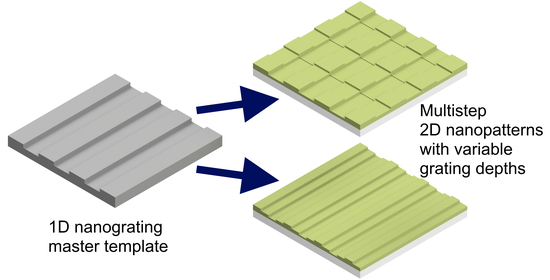
Figure 1.
Overview over the nanopatterning process workflow. Multiple steps of nanoimprint lithography and ion beam etching lead to a multi-dimensional nanopattern with variable feature height.
Figure 1.
Overview over the nanopatterning process workflow. Multiple steps of nanoimprint lithography and ion beam etching lead to a multi-dimensional nanopattern with variable feature height.
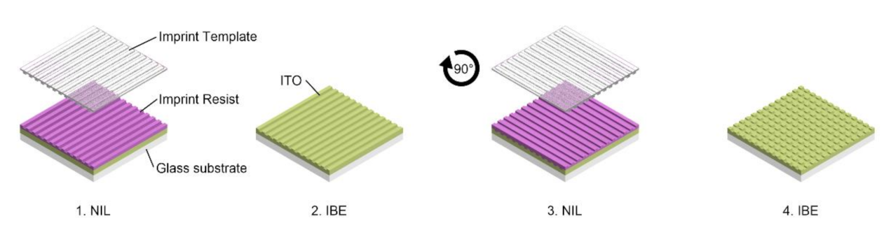
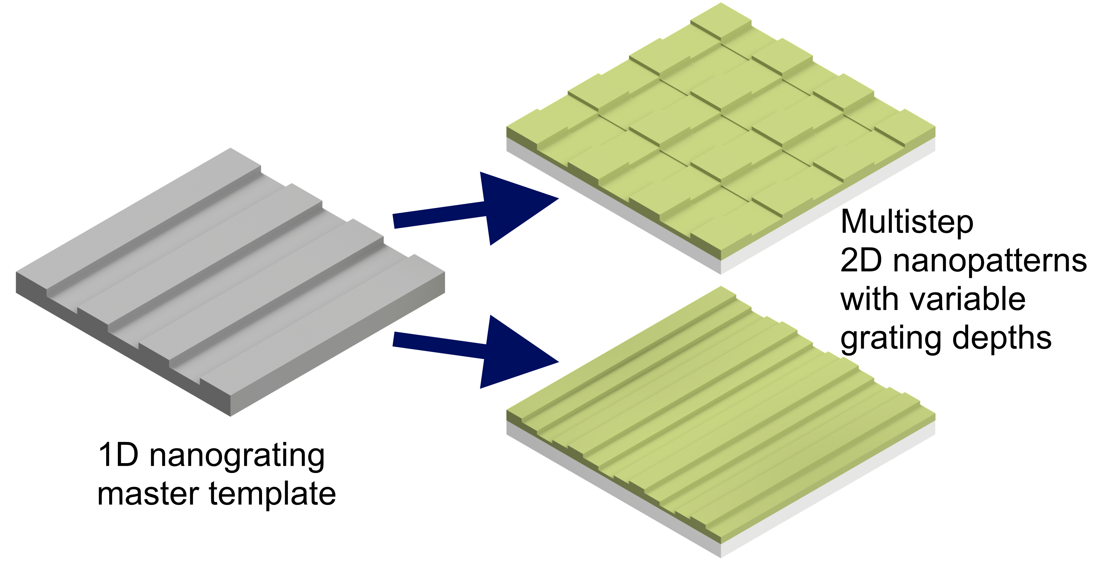
Figure 2.
Digital photograph of a nanopatterned indium tin oxide (ITO) layer comprising a two-dimensional greyscale grating with 600 nm period length. Colorful grating diffraction of reflected light is visible on almost the entire surface area of 25 × 25 mm².
Figure 2.
Digital photograph of a nanopatterned indium tin oxide (ITO) layer comprising a two-dimensional greyscale grating with 600 nm period length. Colorful grating diffraction of reflected light is visible on almost the entire surface area of 25 × 25 mm².

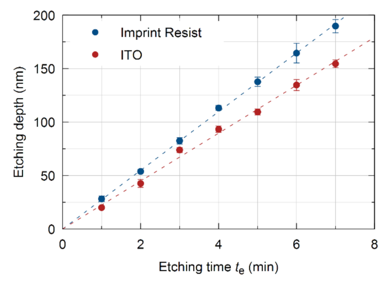
Figure 3.
Etching depth on planar samples coated with ITO and imprint resist. The resulting etching rates are 27.4 nm/min for the imprint resist and 22.4 nm/min for the ITO coating.
Figure 3.
Etching depth on planar samples coated with ITO and imprint resist. The resulting etching rates are 27.4 nm/min for the imprint resist and 22.4 nm/min for the ITO coating.

Figure 4.
(a) Representation of the complete etching process by TOF-SIMS. Zr counts correspond to etching of the imprint resist, whereas In counts correspond to etching of ITO. Si counts correspond to both etching of the imprint resist and the glass substrate as well as a SiO2 passivation layer underneath the ITO coating. Cooling phases of 4 min are introduced after 6 min of etching to avoid thermal damage to the samples. (b) We assume the total etching time required for complete removal of the individual layers to be close to the full width at half maximum of the corresponding ion count.

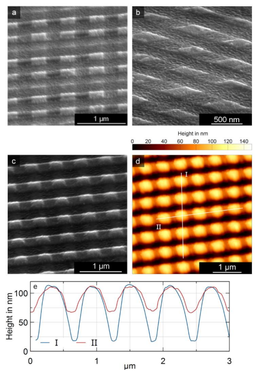
Figure 5.
Scanning electron microscopy (SEM) images of greyscale two-dimensional nanopatterns fabricated with the method described above: (a) rectangular pillar pattern with period lengths 400 nm and 600 nm, (b) rhomboid pillar pattern with period length 500 nm at a 40° angle, (c) square pillar pattern with period length 600 nm. (d,e) Atomic force microscopy (AFM) measurement of the pattern depicted in (c). The grating depth along grating directions I and II is approximately 90 nm and 40 nm, respectively.

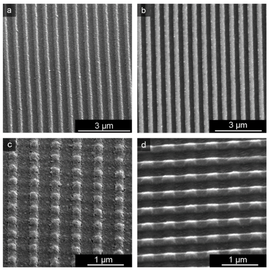
Figure 6.
Comparison of imprinted resist coated with a thin Ag layer for SEM imaging (left side) and etched ITO imprint templates (right side): (a,b) one-dimensional grating pattern with period length 600 nm. (c,d) square pillar pattern with period length 600 nm. Differences visible in the shape of the square pillar patterns presented in (c,d) are caused by the differences in viewing angles.
Publisher’s Note: MDPI stays neutral with regard to jurisdictional claims in published maps and institutional affiliations. |
© 2021 by the authors. Licensee MDPI, Basel, Switzerland. This article is an open access article distributed under the terms and conditions of the Creative Commons Attribution (CC BY) license (https://creativecommons.org/licenses/by/4.0/).
Share and Cite
MDPI and ACS Style
Buhl, J.; Yoo, D.; Köpke, M.; Gerken, M. Two-Dimensional Nanograting Fabrication by Multistep Nanoimprint Lithography and Ion Beam Etching. Nanomanufacturing 2021, 1, 39-48. https://0-doi-org.brum.beds.ac.uk/10.3390/nanomanufacturing1010004
AMA Style
Buhl J, Yoo D, Köpke M, Gerken M. Two-Dimensional Nanograting Fabrication by Multistep Nanoimprint Lithography and Ion Beam Etching. Nanomanufacturing. 2021; 1(1):39-48. https://0-doi-org.brum.beds.ac.uk/10.3390/nanomanufacturing1010004
Chicago/Turabian StyleBuhl, Janek, Danbi Yoo, Markus Köpke, and Martina Gerken. 2021. "Two-Dimensional Nanograting Fabrication by Multistep Nanoimprint Lithography and Ion Beam Etching" Nanomanufacturing 1, no. 1: 39-48. https://0-doi-org.brum.beds.ac.uk/10.3390/nanomanufacturing1010004