
Silicon Nitride Interface Engineering for Fermi Level Depinning and Realization of Dopant-Free MOSFETs


Institute of Semiconductor Electronics, RWTH Aachen University, Sommerfeldstr. 18, 52074 Aachen, Germany
*
Authors to whom correspondence should be addressed.
†
These authors contributed equally to this work.
Micro 2021, 1(2), 228-241; https://0-doi-org.brum.beds.ac.uk/10.3390/micro1020017
Submission received: 10 October 2021
/
Revised: 12 November 2021
/
Accepted: 15 November 2021
/
Published: 21 November 2021
(This article belongs to the Special Issue Innovative Methods for Semiconductor Doping)
Abstract
:Problems with doping in nanoscale devices or low temperature applications are widely known. Our approach to replace the degenerate doping in source/drain (S/D)-contacts is silicon nitride interface engineering. We measured Schottky diodes and MOSFETs with very thin silicon nitride layers in between silicon and metal. Al/SiN/p-Si diodes show Fermi level depinning with increasing SiN thickness. The diode fabricated with rapid thermal nitridation at 900 C reaches the theoretical value of the Schottky barrier to the conduction band eV. As a result, the contact resistivity decreases and the ambipolar behavior can be suppressed. Schottky barrier MOSFETs with depinned S/D-contacts consisting of a thin silicon nitride layer and contact metals with different work functions are fabricated to demonstrate unipolar behavior. We presented n-type behavior with Al and p-type behavior with Co on samples which only distinguish by the contact metal. Thus, the thermally grown SiN layers are a useful method suppress Fermi level pinning and enable reconfigurable contacts by choosing an appropriate metal.
1. Introduction
The ability to modify the conductivity of semiconductors with impurity doping is one of the central ingredients of modern complementary metal-oxide-semiconductor (CMOS) technology enabling electron, as well as hole conduction, p-n-junctions, bi-polar, and field-effect transistors (FETs). However, in today’s deep nanoscale MOSFETs even at very high dopant concentrations only a few dopants reside in typical source/drain contact volumes resulting in strong variability of the electrical device characteristics [1]. Furthermore, the nanoscale size leads to an increase in the ionization energy of dopants due to a dielectric mismatch [2,3,4], as well as dielectric and quantum confinement effects [5,6]. In turn, this yields increasing parasitic source/drain resistances with decreasing spatial dimensions of devices. Although a mere replacement of doped regions with metals appears attractive, the Schottky barrier that forms at metal-semiconductor contacts due to Fermi level pinning severely impacts the electrical behavior of FETs: So-called Schottky barrier devices exhibit a deteriorated off-state with impaired switching and high leakage, as well as a lower on-state performance compared to conventional FETs with doped source/drain electrodes. As a result, alternatives to impurity doping are much sought-after.
A promising approach to replace impurity doping with metals is to reduce the impact of the Schottky barrier by depinning the Fermi level. This can be accomplished by inserting an ultrathin insulator in-between the metal and the semiconductor [1,7,8,9,10]. This interlayer strongly reduces the density of so-called metal-induced gap states (MIGS) that are the main reason for Fermi level pinning [11,12,13]. In addition, the dangling bonds at the silicon surface are saturated with the interlayer material [14,15]. In addition, when bringing two materials in contact, physical changes, e.g., mechanical stress or change of micro hardness can appear in each material due to the formation of a contact layer [16,17]. However, mechanical stress of the contact metal in use (Al) is small for our measurement conditions at room temperature. Because of that, these effects are not explained in more detail. In contrast, metallurgical reactions [18] are considered as they change the electrical behavior of the semiconductor device.
Ultrathin layers grown with rapid thermal nitridation (RTN) are a promising interlayer material because of their fabrication and material properties. On the one hand, the nitridation of silicon surfaces can be carried out at uncritical process temperatures as a chemical reaction between silicon and already starts to occur at 100 K [19]. The growth of silicon nitride (SiN) layers with a temperature dependent self-limiting process gives the advantage of very high tunability and reproducibility of the silicon nitride layer thickness between 0.8 nm and 2 nm. Since, the silicon nitride surfaces act as a diffusion barrier that helps to prevent further unintended oxidation of the silicon surface the reproducibility of subsequent fabrication steps is improved as well. On the other hand, the SiN band gap is large enough to block MIGS and in addition has a moderate potential barrier of approximately 2 eV with respect to the silicon conduction and valence band which enables a high tunnel probability into each [20] and the flexibility to choose n- or p-type behavior independent of the interlayer material. In recent works, dopant-free ohmic contacts and p- or n-like switching behavior of Schottky barrier MOSFETs (SB-MOSFETs) were observed by using thermally grown silicon nitride [9,21,22]. By depinning the Fermi level with a 0.8 nm SiN layer different metal work functions were used to show unipolar n- and p-like switching behavior and ohmic current behavior [22].
In the present publication, we study the Schottky barrier height of Al/SiN/p-Si contacts modification with different SiN interlayers. Furthermore, we show the impact of this interface engineering towards the switching behavior of pseudo and top gate MOSFETs with metals with high and low work function in order to realize n- and p-type switching behavior with the same interlayer.
1.1. Metal-Semiconductor Contacts
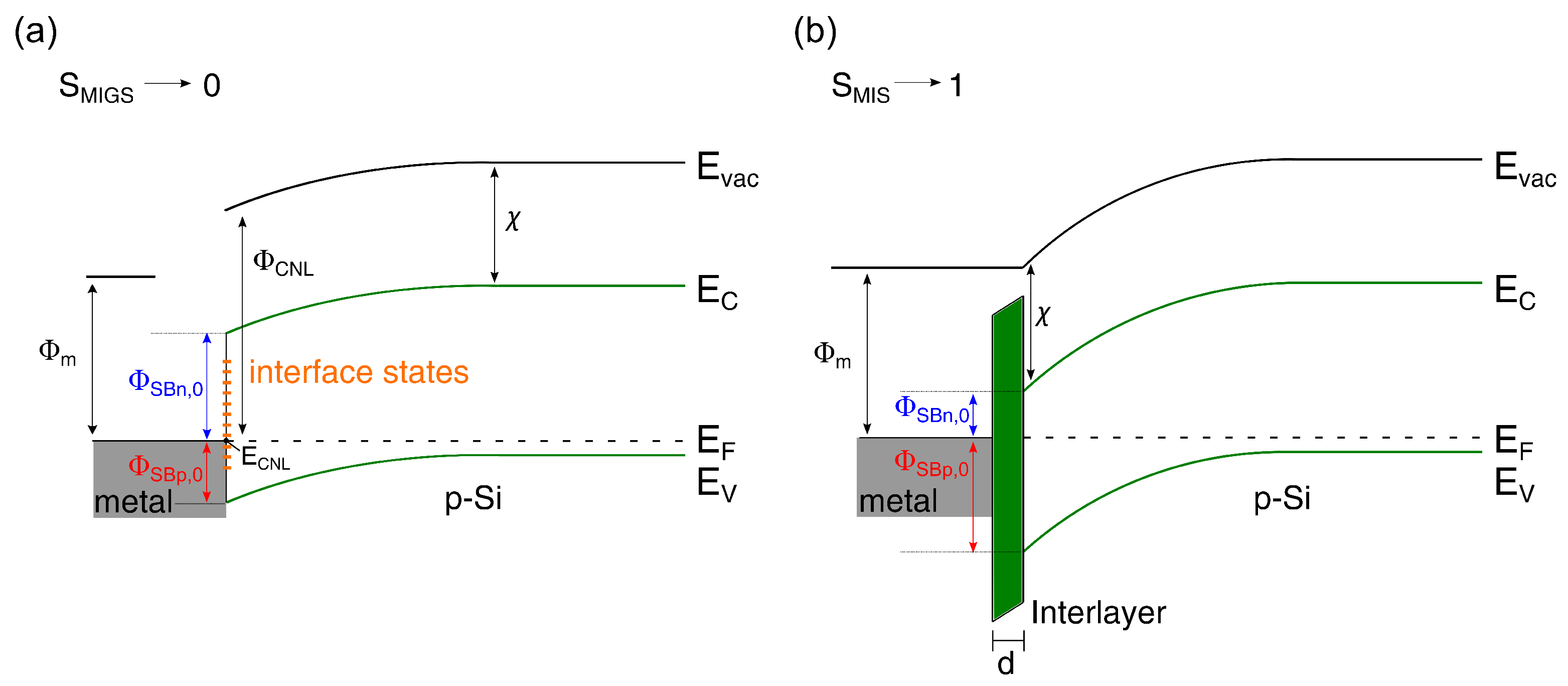
Schottky barriers at a metal-semiconductor interface strongly deteriorate the electrical behavior of SB-MOSFETs as they cause high contact resistances and ambipolar switching behavior. In literature, there has been a long debate whether unsaturated dangling bonds and defects at the silicon surface or the MIGS are responsible for Fermi level pinning [21,23,24,25,26,27]. The current understanding is that MIGS are the dominant factor leading to Fermi level pinning at metal semiconductor interfaces in the vicinity of the charge neutrality level of the semiconductor [13]. MIGS decay into the band gap of the semiconductor when a metal comes into contact with the semiconductor surface [11] (see Figure 1a). When Fermi level pinning is overcome with interface engineering, the metal work function can be used to adjust the effective barrier height (see Figure 1b).
The ability to change the Schottky barrier height at a metal-semiconductor interface by the metal work function is described by the pinning factor with
where q is the electric charge, the vacuum permittivity and is the relative permittivity of the material of which the Fermi level is pinned. and are the density of MIGS at the interface and the decay length, respectively, given by:
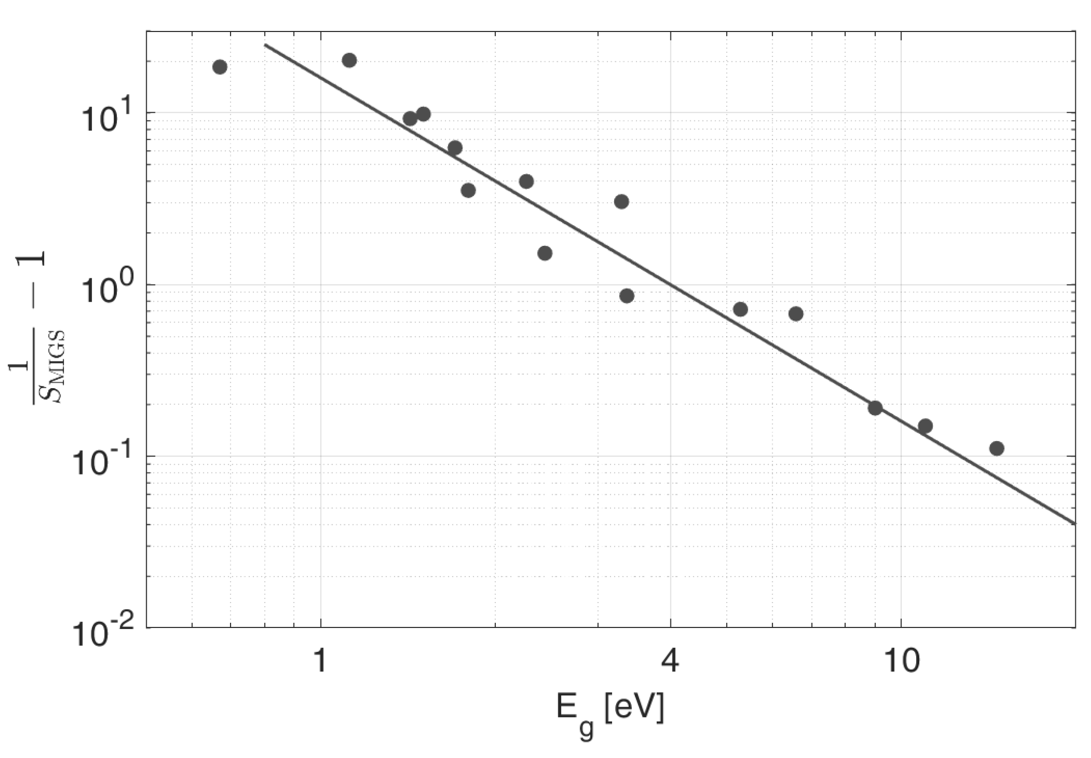
with h being Planck’s constant, the free electron mass, a the lattice constant and the band gap of the semiconductor. If the decay length in Equation (2) is interpreted as the thickness of the interface layer the metal-semiconductor contact can be regarded as a metal-insulator-semiconductor (MIS) capacitor. As a result, Equation (1) provides the change of surface potential (i.e., ) with changing gate potential () given by with and being the density of MIGS and interface layer capacitors per area, respectively. If , tends to zero, the Schottky barrier is hardly changed and hence the Fermi level is pinned. On the other hand, in the case , and the so-called Schottky–Mott limit is reached [11,12,13,23]. Since both as well as are inversely proportional to , Fermi level pinning occurs in materials with small band gaps. Insulators on the other hand are more or less depinned due to their large . Figure 2 shows the pinning factor extracted from literature values for different insulators and semiconductors as a function of their band gap.
An effective work function that determines the band alignment of the Schottky contact can be described with help of the pinning factor [7,12,13]:
with being the potential between and the vacuum level . The charge neutrality level is the energy level at the interface due to the charge transfer between metal and semiconductor to compensate for surface states. Therefore, placing an interface layer with large band gap on top of a semiconductor with small allows removing Fermi level pinning. In the following this will be discussed in more detail.
1.1.1. Pinning Behavior without Interlayer ( → 0)
From Figure 2, the pinning factor for silicon ( = 1.12 eV) of can be extracted resulting in rather strong Fermi level pinning. Hence, the Schottky barrier height is nearly independent of the metal work function in use and the potential at the interface changes only slightly around the charge neutrality level . Typical Schottky barriers at a pinned interface on n-Si are eV and eV with respect to the conduction and valence band, respectively, for metals with a rather high work function (see Figure 1a) [12,18].
1.1.2. Pinning Behavior with Interlayer ( → 1) and Choice of Material
If an interlayer of thickness d is present, the density of MIGS at the metal-interlayer interface decays exponentially across the interlayer. As a result, the reduced density of MIGS at the interlayer-silicon interface is a function of the interlayer thickness which is given by:
where is the decay length of the interlayer.
From Equation (1) and Equation (4) the Fermi level pinning at the interlayer-semiconductor interface is then given by [11,23]:
with the electric permittivity of the interlayer.
Since the interlayer has its own intrinsic pinning factor calculated according to Equation (1), combining the intrinsic pinning factor of the interlayer and the interlayer dependent pinning factor of the semiconductor, Equation (5) is extended to the effective pinning factor of the whole MIS structure [23]:
Equation (6) suggests that Fermi level depinning can be achieved either with , or . However, one has to keep in mind that this yields an exponentially reduced transmission of carriers (cf. Equations (1) and (2)) and hence unacceptably high contact resistivities as confirmed with Wentzel–Kramers–Brillouin (WKB) simulations [23].
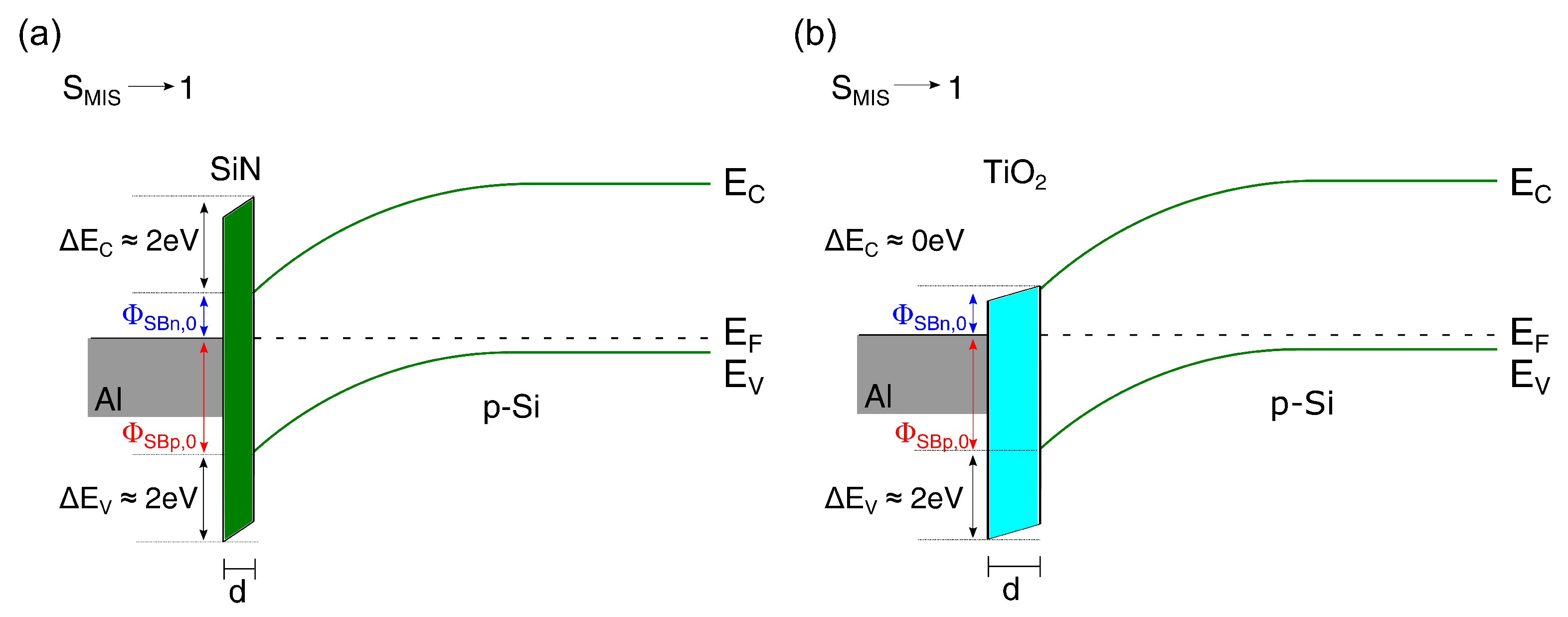
Another important point needs to be mentioned at this stage of the discussion: When searching for an appropriate interface material, the band alignment between the silicon bands and the interlayer is critical. It appears preferable to choose an insulator with high band gap but small conduction or valence band offsets in order to obtain proper contacts to the conduction and valence bands, respectively (cf. Figure 3b) [13,23]. Simulations [1,28] and experiments [23] show that TiO and even more ZnO are materials that yield substantially improved n-type contacts while blocking holes. Materials with band alignment close to the valence band could be NiO or CuAlO [7,28] which has been confirmed experimentally [28]. However, the band gaps of the mentioned materials are rather small (3.2–3.6 eV) and the charge neutrality point of, e.g., ZnO is close to the conduction band. As a result, the demonstrated low contact resistivities of ZnO and TiO are rather due to a repinning of the Fermi level close to the conduction band. Hence, for proper n-type and p-type contacts on the same chip, two different materials are required. However, from a fabrication point of view, this requirement of two different, very thin insulators is a drawback. Moreover, during deposition of oxides (such as the TiO, ZnO, NiO, etc.) and a possible subsequent annealing step, a SiO layer usually forms that will impact the respective contact properties.
In the case considered here, we aim at using a single material as depinning layer. To this end, Fermi level repinning at the metal-interlayer interface needs to be avoided. Taking into consideration that typical metals cover a work function range of approximately 2.5 eV and that the Schottky barrier needs to be modified across the band gap of silicon, a material satisfying eV/2.5 eV = 0.45 (cf. Equation (1)) needs to be chosen. From Figure 2, it is apparent that the band gap of such an interlayer needs to be eV. Silicon nitride with a band gap of 5.1 eV, a conduction band offset of ≈2 eV and the fact that extremely thin layers can be grown thermally with high precision and reproducibility that prevent oxide growth of the silicon surface make SiN an ideal candidate material as depinning layer (cf. Figure 3a).
2. Materials and Methods
2.1. Fabrication of Schottky Diodes
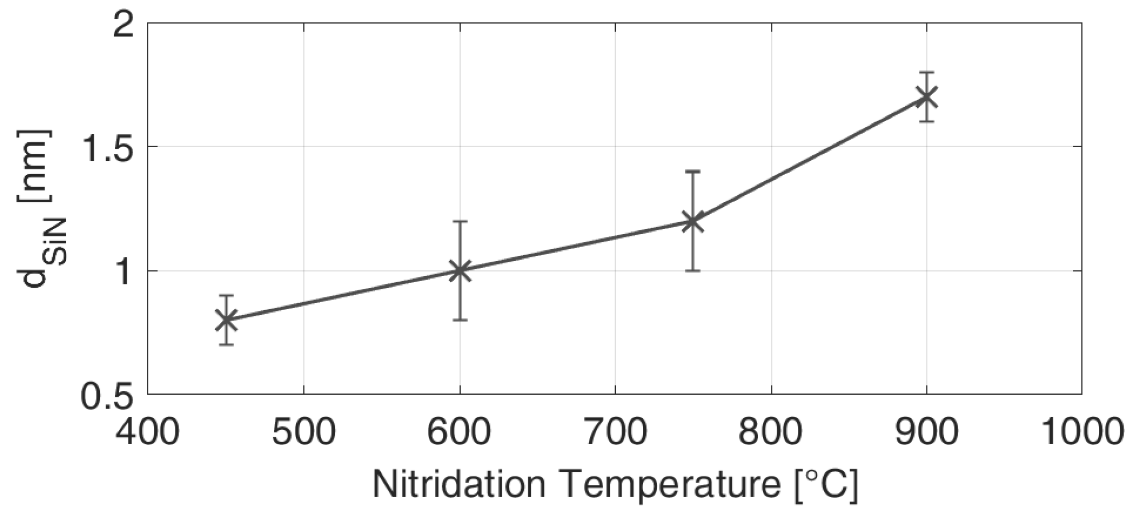
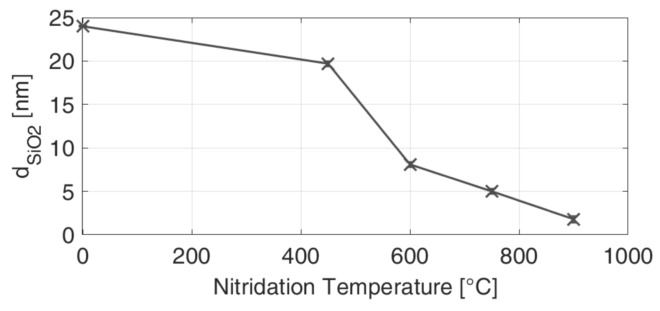
Al/SiN/p-type Si Schottky diodes were fabricated without and with SiN interlayers in order to investigate the Fermi level depinning as a function of thermally grown SiN layer thickness. A 50 nm p-doped silicon-on-insulator (SOI) with a resistivity of 5–10 cm and a buried oxide (BOX) layer of 100 nm substrate was used. The SOI layer was patterned into mesa structures using optical lithography and a / dry etching process. Subsequently, another optical lithography and ion implantation of boron with a dose of 5 × 10 cm at 2 kV acceleration voltage were carried out in order to realize one ohmic contact region for each Schottky diode. After resist ashing and a Piranha clean (:), the dopants were activated at 940 C for 13 s in 2000 sccm Ar at 1000 mbar in a rapid thermal annealing tool. ECV measurements of dummy samples implanted and activated with the same parameters confirm a doping concentration of 9 × 10 cm at the doped Si surface. Prior to the fabrication of the SiN layer, a RCA-clean at 80 C [29] was performed followed by a short HF-dip (1%) immediately before the nitridation process in order to remove the native oxide from the silicon surface. Rapid thermal nitridation in 2000 sccm ammonia () at 1000 mbar for 60 s at different temperatures was conducted in order to grow the SiN layers. The resulting thickness of the SiN layer can be adjusted very precisely by varying the temperature of the process (see Figure 4) as the diffusion of nitrogen through the grown SiN layer is a self-saturating process where the maximal diffusion length depends almost exclusively on the temperature. Since the temperature does not only influence the thickness but also the quality of the SiN layer, as the dissociation of is dependent on temperature as well, the different SiN layers will be referred to their growth temperature and not their thickness.
The metal contacts were fabricated by a deposition of 150 nm Al on top of the whole sample surface with electron-beam physical vapor deposition (EBPVD). Subsequently, the Al film was patterned with optical lithography and commercially available Al etch (TechniEtch Al80, MicroChemicals) to form the Schottky contacts. Afterwards, optical lithography and a buffered oxide etch (BOE) were performed, to etch the SiN (and native oxide in case of the reference sample without interlayer) in order to open the ohmic contact areas for metallization. After resist removal with aceton and isopropanol, samples were immediately mounted for EBPVD of 150 nm Al followed by structuring the ohmic contacts with optical lithography and Al wet etch. Finally, a post metal annealing (PMA) in / forming gas at 400 C for 30 min was performed. In order to characterize the impact of the PMA process, I–V measurements were taken before and after PMA. The measurements were carried out with a Keithley 4200-SCS parameter analyzer using two pre-amplifiers. Figure 5 shows the schematic cross-section of the Schottky diode.
2.2. Fabrication of Schottky Barrier MOSFETs
Characteristic of Schottky barrier MOSFETs are Schottky S/D-contacts without additional doping. So the fabrication of such devices reduces to the following: The SOI substrate consist of SOI: cm Boron doped 80 nm p-Si and 2 m BOX. The structuring of the Si mesa structures was performed as described above. After resist ashing, a Piranha clean with subsequent RCA-process was carried out. An HF-dip removed the native oxide immediately before the rapid thermal nitridation process (300 sccm /1000 sccm Ar gas mixture at 1000 mbar for 60 s, Annealsys AS-One system (Montpellier, France)). When using Al as a contact metal, 150 nm Al were deposited with EBPVD on the whole sample surface and the contacts were patterned, as described above. When using Co as a contact metal, the samples were patterned with optical lithography to perform a lift-off process after 150 nm EBPVD deposition of Co. The samples have not been annealed after contact formation. In its simplest form, the handle wafer of the SOI wafer can be used as large area back gate yielding a so-called pseudo MOSFET as schematically shown in Figure 6a.
In order to fabricate top gate MOSFETs, processing continued with atomic layer deposition (ALD) at 300 C of 20 nm as the gate oxide. Afterwards, 150 nm Al as gate metal have been EBPVD deposited and top gate structures have been patterned with optical lithography and wet chemical etching of Al as described before. Finally, a PMA was performed in / for 30 min at 400 C. It should be mentioned that due to the fabrication process the area underneath the gate electrode is covered with SiN between Si and , too. A schematic cross-section of a top gated Schottky barrier MOSFETs is shown in Figure 6b.
2.3. Extraction of Schottky Barrier Heights
The forward current characteristics of a Schottky diode described by the thermionic emission model [12] is given by Equation (7) which is valid for voltages .
where V is the voltage across the diode, k the Boltzmann constant and T the absolute temperature. n is a dimensionless ideality factor, that takes non-idealistic diode behavior into account. is the so-called saturation current [30] that is defined as:
with A being the effective contact area, the effective Richardson constant and the Schottky barrier height. The Richardson constant is defined as:
with being the effective mass of the charge carriers. Experimental values differ slightly from the calculated values so that for practical applications can be considered as 30 A cm K for p-doped silicon and 110 A cm K for n-doped Silicon [12]. Taking into account the series resistance of the diode by considering the device as a series combination of the diode and a resistor with resistance R, the voltage across the diode V will be replaced by with being the applied voltage leading to Equation (7)
The Schottky barrier was extracted by the method presented by Cheung and Cheung [31]. This method has the benefit that the Schottky barrier, ideality factor and series resistance can be obtained by a single I-V measurement of the forward current. Combining Equation (8) to (10), using the current density J instead of the current I and solving for gives
Then, computing the derivative yields
As a result, plotting the derivative of experimental data as a function of J yields as the slope and as the y-axis intercept, and, thus, enables obtaining R and n. In order to extract the Schottky barrier , a function is defined with help of Equation (11) giving another linear dependency:
Here, the y-axis intercept will give the Schottky barrier with n determined as discussed above. Furthermore, the slope of the plot will be again. Comparing the resistance values extracted from the two plots allows reconfirming the results and hence the consistency of the method.
In addition to the approach detailed so far, a simple method for the extraction of and n based on Equation (7) is performed. Plotting over gives the slope of the linear region as and the saturation current as the y-axis intercept [30]. The Schottky barrier is then extracted by solving Equation (8) for . The values of both methods are compared for verification of the results.
3. Results and Discussion
3.1. Schottky Barrier Height for Different SiN Interlayers
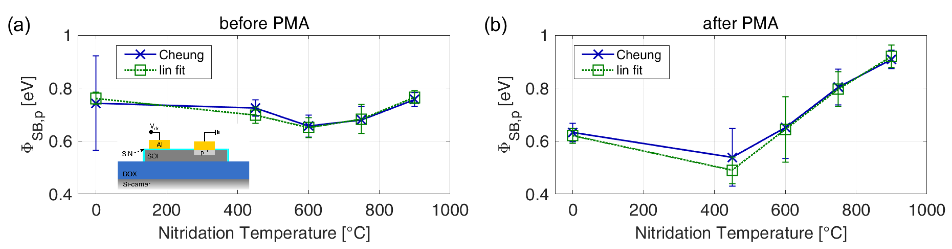
The Schottky barrier height is extracted from Schottky diodes with different SiN interlayer thicknesses before and after PMA. Before PMA (Figure 7a), a dependency of the Schottky barrier on the interlayer thickness does not emerge clearly. is around 0.75 eV for the reference sample (compared to [32]), 450 C SiN interlayer and 900 C SiN interlayer and decreases to 0.65 eV for the diodes with SiN fabricated at 600 C and 750 C. After PMA (Figure 7b), the contact properties change dependent on the interlayer.
The Schottky barrier heights of the reference sample without an interlayer and the sample with thinnest (450 C) SiN decrease with respect to the valence band to 0.63 eV and 0.51 eV, respectively, so that it is closer to the middle of the band gap. The barrier height of the SiN fabricated at 600 C stays the same (0.65 eV) while it increases for the samples with thicker SiN layers, resulting in a small barrier to the conduction band (). A SiN layer fabricated at 750 C lowers the barrier to the conduction band to 0.32 eV after PMA. The thickest layer fabricated at 900 C reduces the Schottky barrier to the conduction band to 0.2 eV which is the expected ideal value from with eV and eV. For further consideration of the influence of each SiN layer to the contact properties, the ideality factor and series resistance extracted from the same measurements should be evaluated.
3.2. Ideality Factor and Series Resistance
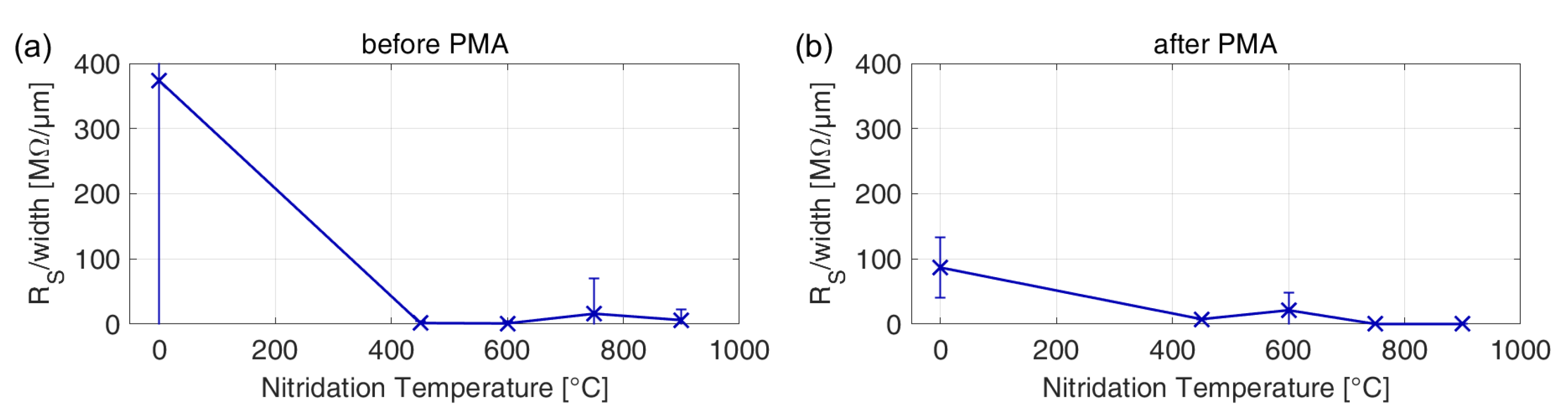
Without PMA, the series resistance for the Schottky barrier without a SiN interlayer is two orders of magnitude larger (374 M/m) than with a SiN interlayer (Figure 8a). It decreases after PMA, but still is much higher than the resistance of the devices with an interlayer. When having an interlayer, the values vary between 1 M/m and 16 M/m without PMA. The resistance and its deviations are smaller for thin SiN layers. After PMA (Figure 8b), the series resistance decreases for thicker layers towards 0.1 M/m, which is comparable to the magnitude of the resistance of the silicon channels of the SOI substrate without any applied gate voltage.
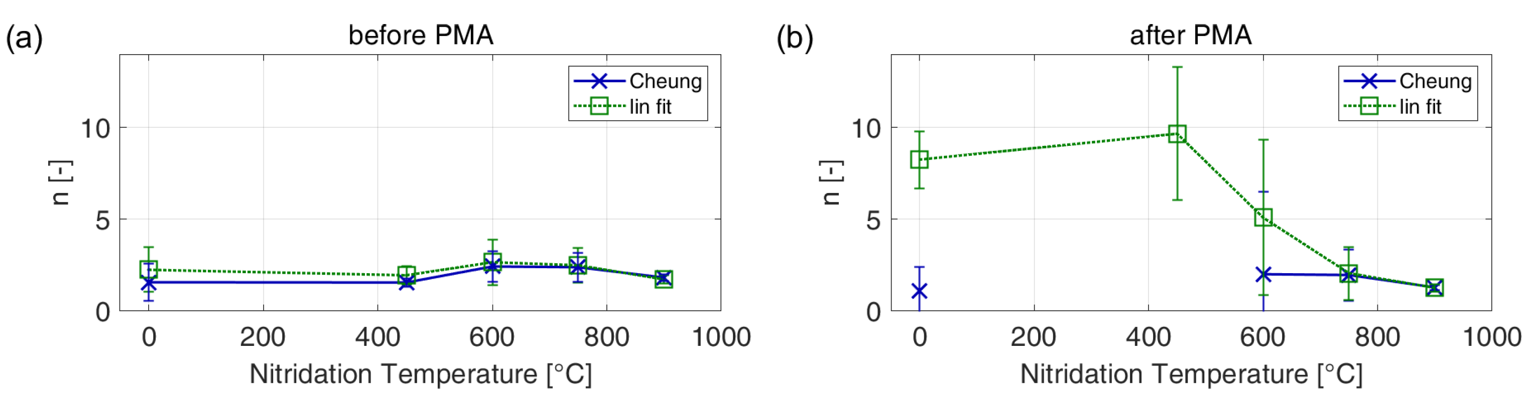
However, for both thin SiN layers (450 C and 600 C), the series resistance has increased to 7 M/m and 21 M/m, respectively, though the tunnel probability increases for decreasing thickness of an interlayer [12]. The resistance of the 600 C SiN layer device has not only increased, but so has the deviation. Considering the ideality factor (Figure 9), it is obvious, that these values differ from the expected behavior in the same way, since the ideality factor (Figure 9) increases to unreasonably high values with high deviations ( nm and 600 C SiN) or n is not even evaluable anymore (450 C) with Cheung’s method.
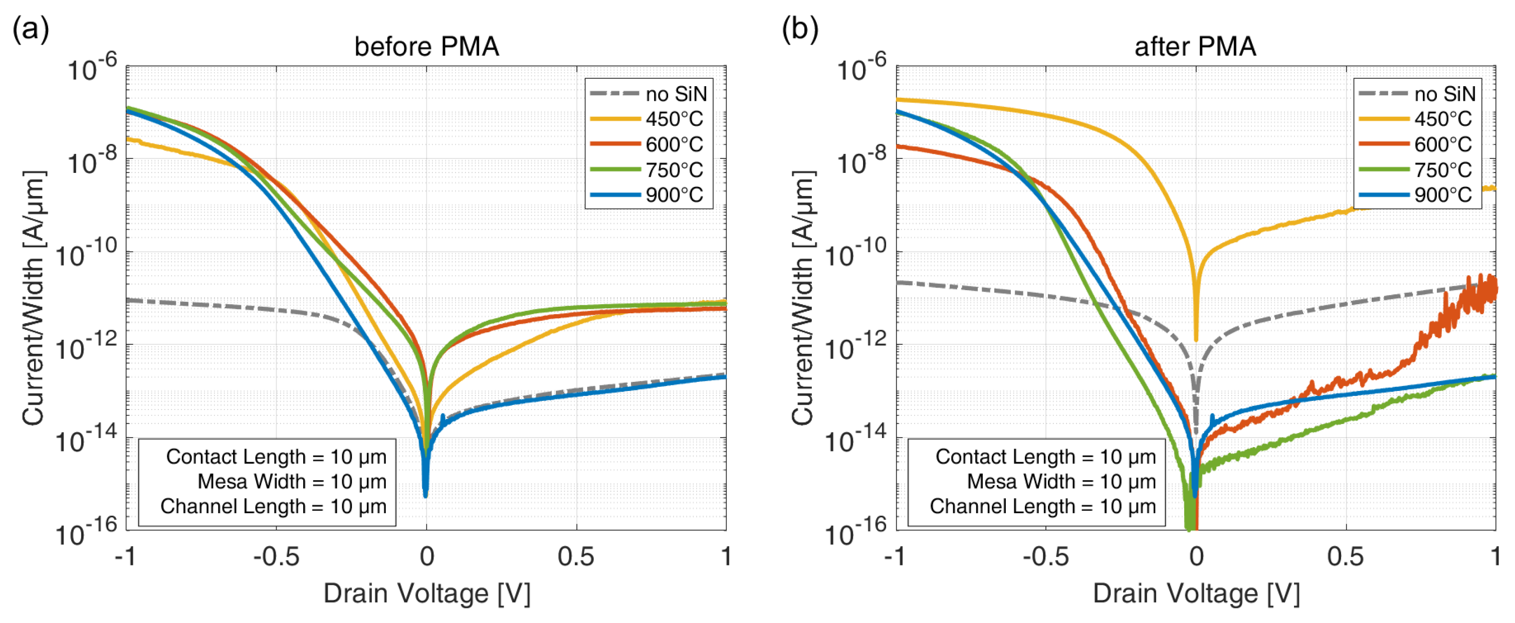
The review of a single --measurement of each contact layer stack gives the reason for the differing behavior with regard to the ideality factor and series resistance. The ideal diode behavior with an exponential increase (linear regime in logarithmic scale) in forward direction for until the series resistance dominates the current flow and a low reverse current is visible for all measurements before PMA (Figure 10a).
However, after PMA (Figure 10b), the - behavior of the samples without an interlayer and with the 450 C SiN changes. An exponential increase in the current of the reference sample is not visible anymore and the reverse current is as high as the forward current. A linear plot would reveal a linear and symmetric - behavior. The low absolute current can be explained by the high series resistance. For the sample with the 450 C SiN layer the reverse current has increased severely and the forward current is rather linear than exponential.
Al/Si contacts without an interlayer are known to undergo a metallurgical reaction in high temperature processes [33]. After dissolving in aluminum up to its solubility limit during the high temperature process [34], silicon recrystallizes epitaxially at the Al/Si interface when it is cooled. This recrystallized silicon is heavily doped with Al [18], so a p-type layer has been formed resulting in a nearly ohmic contact at the Schottky barrier side of the device.
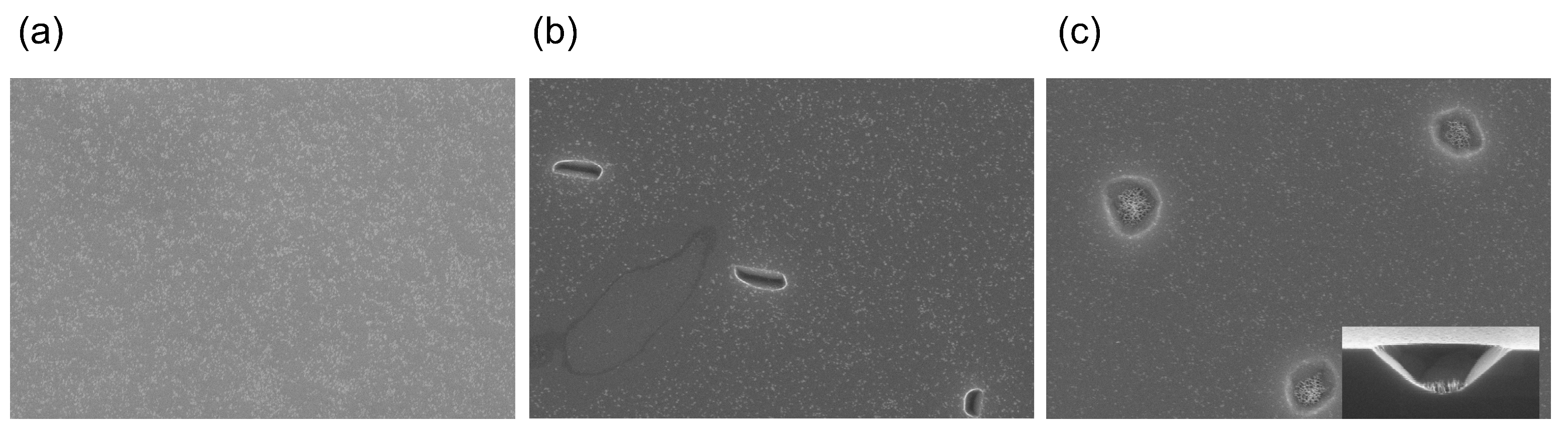
In order to find out why the diodes with the 450 C SiN interlayer, that should act as a diffusion barrier, show similar - behavior to the sample without interlayer, the SiN layers are investigated more thoroughly. The lower the temperature of the rapid thermal nitridation process, the higher is the hydrogen amount in the SiN layer [35]. A higher hydrogen concentration deteriorates the insulating properties [35]. Another observation is that the 450 C SiN layer allows diffusion of oxygen during high temperature processes. In order to evaluate the physical barrier properties of the SiN layers, two tests were conducted. First, a Al/SiN/Si layer stack was fabricated compared to the diode process (but with a gas mixture for nitridation of 300 sccm /1000 sccm Ar). After PMA, the Al was wet chemically etched. SEM pictures (Figure 11) show a strong deterioration of the Si surface for the reference sample and of the Si/SiN surface of the one with the 450 C SiN layer. When the SiN layer is not completely closed, Si will dissolve into Al and diffuse at the Al/SiN interface. Sankur et al. [36] measured that the effect of recrystallization is stronger at reentrant corners compared to a flat surface. Thus, the SEM pictures support the assumption of an metallurgical reaction on the contact area of the 450 C SiN interlayer sample so that islands of strongly p-doped Si form after PMA, leading to an overcoming of the Schottky barrier towards a p-type ohmic behavior.
Second, the diffusion barrier of the SiN layers was characterized by a thermal oxidation process. This method has been used before [37] in order to characterize the density of SiN layers. The samples were fabricated in the same way as before until the thermal nitridation. Then, just after the thermal nitridation process, without opening the process chamber an oxidation process (1050 C, 2000 sccm , 240 s) was started. The resulting oxide thickness is measured with spectroscopic ellipsometry at multiple wavelengths. Figure 12 shows that the thin SiN layers (450 C and 600 C) hardly prevents the oxidation whereas thicker SiN layers reduce an oxidation drastically. Both tests indicate a porosity of the thin SiN layer.
The large distribution of measured values of , n, and in the case of the C SiN interlayer diode can be ascribed to the same defects observed for the thinnest SiN layer. However, they occur far less so that the defects do not determine the overall diode behavior.
3.3. Electrical Characteristics of SB-MOSFETs with Varying Interlayers
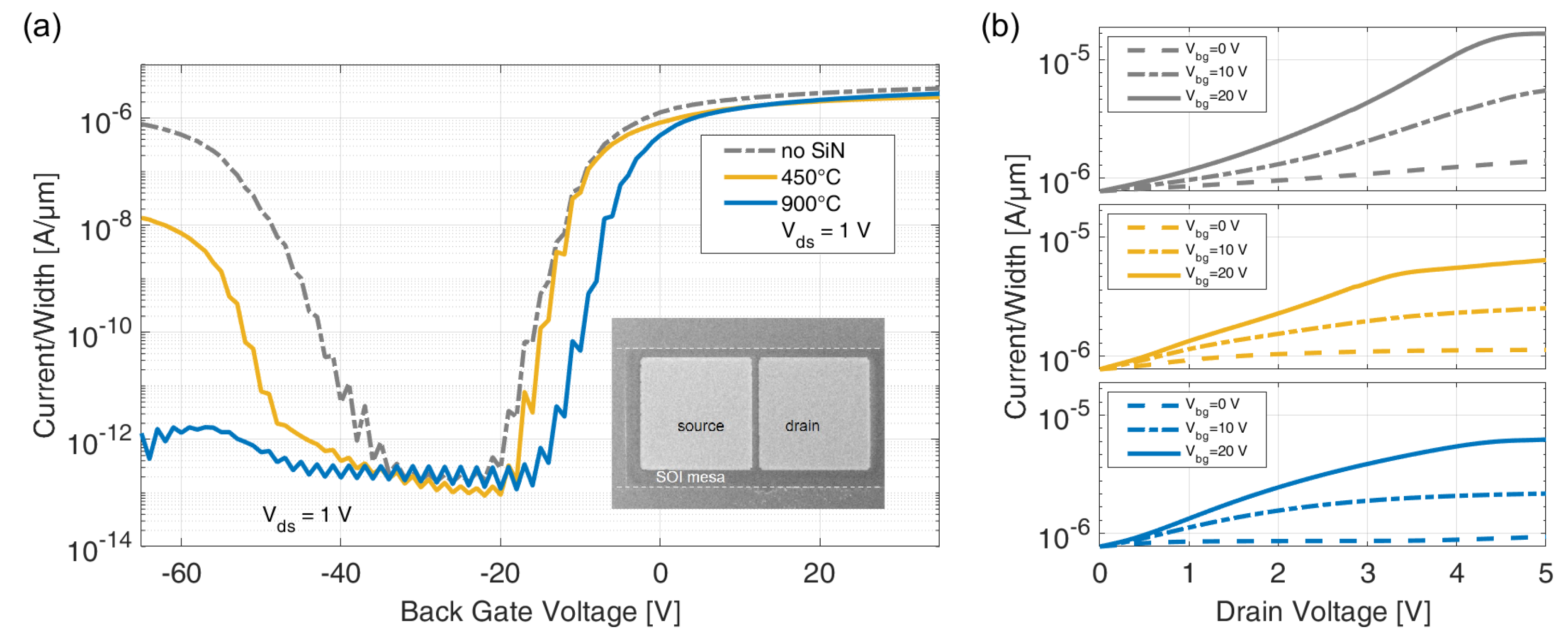
After depinning the Fermi level the work function of different contact metals can be used to obtain n- and p-type MOSFET behavior. Back gate controlled samples (see Figure 6a) have been fabricated without PMA. Figure 13a shows the switching behavior for a 450 C and 900 C SiN interlayer and a reference sample without an interlayer. When applying a back gate voltage to the sample with no interfacial layer, ambipolar switching behavior with no defined off-state is observed. Though the Schottky barrier heights before PMA do not show significant differences when inserting different SiN layers, a change in the switching behavior due to them is observed. For the 900 C SiN interlayer, a strong n-type behavior is observed as the p-type current is strongly suppressed which leads to an -ratio of . In case of the 450 C SiN device the p-branch is less suppressed so that the switching behavior still shows ambipolar behavior but with a reduced p-type current compared to the reference sample. In addition, output characteristics (Figure 13b) show an exponential current increase for the reference sample while the current increases more linearly when adding the SiN interlayers.
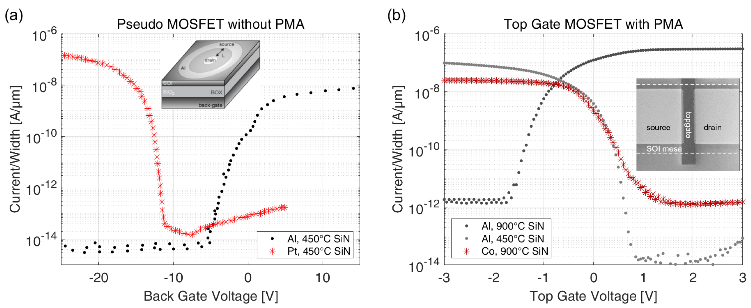
The realization of unipolar switching behavior by modifying the Schottky barrier with Fermi level depinning and choosing a metal with appropriate work function was reported recently by Fischer et al. (Figure 14a). He characterized circular pseudo MOSFETs (p-Si SOI 200 nm, 200 nm BOX, no PMA) not only with Al to have a good contact towards the conduction band but also with Pt as a metal with a high work function.
Using contact metals with higher work functions (e.g., Pt (≈5.65 eV), Ni (≈5.15 eV), Co (≈5 eV) [12]) a reduced Schottky barrier towards the valence band can be provided(). That leads to a more p-type switching behavior as shownin Figure 14a (red curve) with an on-/off-ration of = . As an interlayer a 450 C SiN layer was used. The on current of the Pt device is slightly higher compared to the Al device which implies that the remaining Schottky barrier to the respective band is lower using Pt. Assuming perfect Fermi level depinning the remaining Schottky barrier in case of Pt towards the valence band is eV what means a complete removal of the Schottky barrier between metal and valence band whereas for Al a small barrier of eV remains towards the conduction band.
In order to demonstrate the same functionality on top gate controlled devices, we fabricated and characterized SOI top gate MOSFETs (see Figure 6b). Though Co has a lower work function than Pt, it is still high enough to obtain p-like switching behavior with a 900 C SiN interlayer as shown in Figure 14b. A top gate voltage between −3 V to 3 V has been applied. An inverse subthreshold slope S of 343 mV/dec was measured. As the remaining Schottky barrier to the valence band of a ideal Co/SiN/Si contact with = 0.17 eV is higher compared to the Pt sample, the -ratio () is smaller as well.
The same measurement have been performed to Al contacts with 900 C SiN and 450 C SiN layer. As shown with the pseudo MOSFET measurements in Figure 13, the top gate controlled device with an 900 C SiN layer shows just the same strong n-type behavior in accordance to the reduced Schottky barrier towards the conduction band. Compared to the Co devices, an even steeper switching behavior of 163 mV/dec and is measured. In contrast to the pseudo MOSFET measurements without PMA, the 450 C SiN top gate device with Al contacts shows a p-type switching behavior with a strong suppressed n-type off-state current. This indicates a heavily Al doped silicon at the interface caused by the PMA due to a leaky SiN interface as already discussed above.
4. Conclusions
We measured Schottky barriers of Al/SiN/p-Si diodes showing Fermi level depinning with help of SiN interlayers. Increasing the process temperature at the rapid thermal nitridation process leads to higher thickness and improved layer quality. The diode fabricated at 900 C reaches the theoretical value of the depinned Schottky barrier to the conduction band with Al as a metal of eV. As Fermi level depinning of the Schottky barrier with the SiN interlayer has been proved, metals with different work functions can be used to modify the Schottky barrier. The effect of the modified barrier to the resulting switching behavior has been shown as the Schottky barrier MOSFETs turn from ambipolar to unipolar behavior with increasing interlayer thickness. Furthermore, we presented n-type behavior with Al and p-type behavior with Co with the same SiN interlayer. Thus, thermally grown SiN layers are a useful method suppress Fermi level pinning and enable reconfigurable contacts by choosing an appropriate metal.
Author Contributions
Investigation, B.R., L.H.; Methodology, B.R., L.H.; Supervision, J.K.; Writing—original draft, B.R., L.H.; Writing—review & editing, B.R., L.H., J.K. All authors have read and agreed to the published version of the manuscript.
Funding
This research was funded by Deutsche Forschungsgemeinschaft (DFG) under project numbers KN 545/24-1 and KN 545/29-1.
Data Availability Statement
Data available on request.
Acknowledgments
The authors thank Horst Windgassen for the ALD deposition and ECV measurements and Frank Ludewig and Ulrich Kentsch at the Ion Beam Centre in Dresden, Germany for the ion implantation.
Conflicts of Interest
The authors declare no conflict of interest.
References
- Shine, G.; Saraswat, K.C. Analysis of Atomistic Dopant Variation and Fermi Level Depinning in Nanoscale Contacts. IEEE Trans. Electron Devices 2017, 64, 3768–3774. [Google Scholar] [CrossRef]
- Björk, M.T.; Schmid, H.; Knoch, J.; Riel, H.; Riess, W. Donor deactivation in silicon nanostructures. Nat. Nanotech. 2009, 4, 103–107. [Google Scholar] [CrossRef] [PubMed]
- Calderón, M.J.; Verduijn, J.; Lansbergen, G.P.; Tettamanzi, G.C.; Rogge, S.; Koiller, B. Heterointerface effects on the charging energy of the shallow D—Ground state in silicon: Role of dielectric mismatch. Phys. Rev. B 2010, 82, 075317. [Google Scholar] [CrossRef] [Green Version]
- Mol, J.A.; Salfi, J.; Miwa, J.A.; Simmons, M.Y.; Rogge, S. Interplay between quantum confinement and dielectric mismatch for ultrashallow dopants. Phys. Rev. B 2013, 87, 245417. [Google Scholar] [CrossRef] [Green Version]
- Khanal, D.R.; Yim, J.W.L.; Walukiewicz, W.; Wu, J. Effects of Quantum Confinement on the Doping Limit of Semiconductor Nanowires. Nano Lett. 2007, 7, 1186–1190. [Google Scholar] [CrossRef]
- Diarra, M.; Niquet, Y.M.; Delerue, C.; Allan, G. Ionization energy of donor and acceptor impurities in semiconductor nanowires: Importance of dielectric confinement. Phys. Rev. B 2007, 75, 045301. [Google Scholar] [CrossRef] [Green Version]
- Saraswat, K.C.; Shine, G. Low Resistance Contacts to Nanoscale Semiconductor Devices. ECS Trans. 2016, 75, 513–523. [Google Scholar] [CrossRef]
- Agrawal, A.; Lin, J.; Barth, M.; White, R.; Zheng, B.; Chopra, S.; Gupta, S.; Wang, K.; Gelatos, J.; Mohney, S.E.; et al. Fermi level depinning and contact resistivity reduction using a reduced titania interlayer in n-silicon metal-insulator-semiconductor ohmic contacts. Appl. Phys. Lett. 2014, 104, 112101. [Google Scholar] [CrossRef] [Green Version]
- Connelly, D.; Faulkner, C.; Clifton, P.A.; Grupp, D.E. Fermi-level depinning for low-barrier Schottky source/drain transistors. Appl. Phys. Lett. 2006, 88, 012105. [Google Scholar] [CrossRef]
- Islam, R.; Shine, G.; Saraswat, K.C. Schottky barrier height reduction for holes by Fermi level depinning using metal/nickel oxide/silicon contacts. Appl. Phys. Lett. 2014, 105, 182103. [Google Scholar] [CrossRef] [Green Version]
- Moench, W. On the physics of metal-semiconductor interfaces. Rep. Prog. Phys. 1990, 53, 221–278. [Google Scholar] [CrossRef]
- Sze, S.M.; Ng, K.K. Physics of Semiconductor Devices, 3rd ed.; Wiley-Interscience: Hoboken, NJ, USA, 2007. [Google Scholar]
- Knoch, J. Nanoelectronics; De Gruyter Oldenbourg: Berlin, Germany, 2020. [Google Scholar]
- Xiao, S.; Xu, S. High-Efficiency Silicon Solar Cells—Materials and Devices Physics. Crit. Solid State Mater. Sci. 2014, 39, 277–317. [Google Scholar] [CrossRef]
- Seiffe, J.; Gautero, L.; Hofmann, M.; Rentsch, J.; Preu, R.; Weber, S.; Eichel, R.A. Surface passivation of crystalline silicon by plasma-enhanced chemical vapor deposition double layers of silicon-rich silicon oxynitride and silicon nitride. J. Appl. Phys. 2011, 109, 034105. [Google Scholar] [CrossRef]
- Shen, F.; Ke, L.L. Numerical Study of Coupled Electrical-Thermal-Mechanical-Wear Behavior in Electrical Contacts. Metals 2021, 11, 955. [Google Scholar] [CrossRef]
- Fillon, A.; Abadias, G.; Michel, A.; Jaouen, C.; Villechaise, P. Influence of Phase Transformation on Stress Evolution during Growth of Metal Thin Films on Silicon. Phys. Rev. Lett. 2010, 104, 096101. [Google Scholar] [CrossRef] [PubMed]
- Card, H. Aluminum—Silicon Schottky barriers and ohmic contacts in integrated circuits. IEEE Trans. Electron Devices 1976, 23, 538–544. [Google Scholar] [CrossRef]
- Hlil, E.K.; Kubler, L.; Bischoff, J.L.; Bolmont, D. Photoemission study of ammonia dissociation on Si(100) below 700 K. Phys. Rev. B 1987, 35, 5913–5916. [Google Scholar] [CrossRef] [PubMed]
- Borrel, J.; Hutin, L.; Rozeau, O.; Jaud, M.A.; Martinie, S.; Gregoire, M.; Dubois, E.; Vinet, M. Modeling of Fermi-Level Pinning Alleviation With MIS Contacts: n and pMOSFETs Cointegration Considerations—Part I. IEEE Trans. Electron Devices 2016, 63, 6. [Google Scholar]
- Riederer, F.; Grap, T.; Fischer, S.; Mueller, M.R.; Yamaoka, D.; Sun, B.; Gupta, C.; Kallis, K.T.; Knoch, J. Alternatives for Doping in Nanoscale Field-Effect Transistors. Phys. Status Solidi A 2018, 215, 1700969. [Google Scholar] [CrossRef]
- Fischer, S.; Knoch, J.; Vescan, A. Ultra Thin Silicon Nitride Interface Engineering. Ph.D. Thesis, RWTH Aachen University, Aachen, Germany, 2017. [Google Scholar]
- Gupta, S.; Paramahans Manik, P.; Kesh Mishra, R.; Nainani, A.; Abraham, M.C.; Lodha, S. Contact resistivity reduction through interfacial layer doping in metal-interfacial layer-semiconductor contacts. J. Appl. Phys. 2013, 113, 234505. [Google Scholar] [CrossRef]
- Sankey, O.F.; Allen, R.E.; Dow, J.D. Si/transition-metal Schottky barriers: Fermi-level pinning by Si dangling bonds at interfacial vacancies. Solid State Commun. 1984, 49, 1–5. [Google Scholar] [CrossRef]
- Mönch, W. Barrier heights of real Schottky contacts explained by metal-induced gap states and lateral inhomogeneities. J. Vac. Sci. Technol. B 1999, 17, 1867. [Google Scholar] [CrossRef]
- Heine, V. Theory of Surface States. Phys. Rev. 1965, 138, A1689–A1696. [Google Scholar] [CrossRef]
- Lu, H.; Guo, Y.; Li, H.; Robertson, J. Modeling of surface gap state passivation and Fermi level de-pinning in solar cells. Appl. Phys. Lett. 2019, 114, 222106. [Google Scholar] [CrossRef]
- Islam, R.; Saraswat, K.C. Metal/insulator/semiconductor carrier selective contacts for photovoltaic cells. In Proceedings of the 2014 IEEE 40th Photovoltaic Specialist Conference (PVSC), Denver, CO, USA, 8–13 June 2014; IEEE: New York, NY, USA; pp. 285–289. [Google Scholar] [CrossRef]
- Kern, W. The Evolution of Silicon Wafer Cleaning Technology. J. Electrochem. Soc. 1990, 137, 1887–1892. [Google Scholar] [CrossRef]
- Schroder, D.K. Semiconductor Material and Device Characterization; John Wiley & Sons, Inc.: Hoboken, NJ, USA; pp. i–xv. [CrossRef]
- Cheung, S.K.; Cheung, N.W. Extraction of Schottky diode parameters from forward current-voltage characteristics. Appl. Phys. Lett. 1986, 49, 85–87. [Google Scholar] [CrossRef]
- Card, H. Thermally-induced changes in barrier heights of aluminium contacts to p- and n-type silicon. Solid State Commun. 1975, 16, 87–89. [Google Scholar] [CrossRef]
- McCaldin, J.O.; Sankur, H. Diffusivity and Solubility of Si in the Al Metallization of Integrated Circuits. Appl. Phys. Lett. 1971, 19, 524–527. [Google Scholar] [CrossRef] [Green Version]
- Basterfield, J.; Shannon, J.; Gill, A. The nature of barrier height variations in alloyed Al-Si Schottky barrier diodes. Solid-State Electron. 1975, 18, 290. [Google Scholar] [CrossRef]
- Fischer, S.; Kremer, H.I.; Berghoff, B.; Maß, T.; Taubner, T.; Knoch, J. Dopant-free complementary metal oxide silicon field effect transistors: Dopant-free MOSFETs. Phys. Status Solidi A 2016, 213, 1494–1499. [Google Scholar] [CrossRef]
- Sankur, H.; McCaldin, J.; Devaney, J. Solid-phase epitaxial growth of Si mesas from al metallization. Appl. Phys. Lett. 1973, 22, 64–66. [Google Scholar] [CrossRef] [Green Version]
- Ito, T.; Nozaki, T.; Arakawa, H.; Shinoda, M. Thermally grown silicon nitride films for high-performance MNS devices. Appl. Phys. Lett. 1978, 32, 330–331. [Google Scholar] [CrossRef]
Figure 1.
Band structure at metal-semiconductor contacts: (a) Metal/p-Si Schottky contact exhibiting Fermi level pinning around that occurs due to a high density of interface states consisting of MIGS, as well as possible defects, dangling bonds, etc. (b) Metal/interlayer/p-Si interface: The interlayer blocks MIGS so that the band alignment is determined by the difference of metal work function and silicon electron affinity.

Figure 2.
Pinning factor for different insulators and semiconductors from experimental data as a function of their band gap. The fit shows a dependency between band gap and [13].
Figure 2.
Pinning factor for different insulators and semiconductors from experimental data as a function of their band gap. The fit shows a dependency between band gap and [13].

Figure 3.
Comparison of band alignments for Schottky contacts with (a) a SiN interlayer and (b) a interlayer.
Figure 3.
Comparison of band alignments for Schottky contacts with (a) a SiN interlayer and (b) a interlayer.

Figure 4.
SiN thickness achieved by rapid thermal annealing of Si substrates in at different temperatures for 60 s.
Figure 4.
SiN thickness achieved by rapid thermal annealing of Si substrates in at different temperatures for 60 s.

Figure 5.
Schematic assembly of Schottky diodes with Al/SiN/p-Si Schottky contact and doped ohmic contact.
Figure 5.
Schematic assembly of Schottky diodes with Al/SiN/p-Si Schottky contact and doped ohmic contact.

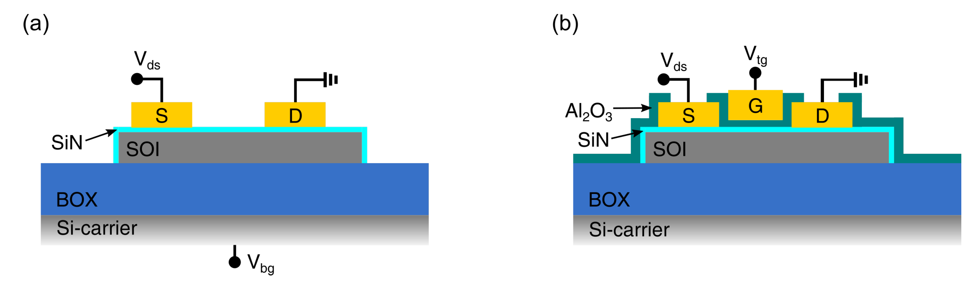
Figure 6.
Schematic cross-sections of Schottky barrier MOSFETs with metal/SiN/p-Si contacts and (a) back gate (pseudo MOSFET) or (b) a top gate electrode.
Figure 6.
Schematic cross-sections of Schottky barrier MOSFETs with metal/SiN/p-Si contacts and (a) back gate (pseudo MOSFET) or (b) a top gate electrode.

Figure 7.
Schottky barrier of devices with different SiN interlayers (a) before PMA and (b) after PMA.
Figure 7.
Schottky barrier of devices with different SiN interlayers (a) before PMA and (b) after PMA.

Figure 8.
Series resistance (a) before PMA and (b) after PMA, extracted by the method of Cheung [31]. The series resistance is given in M/m in order to reduce the error caused by different device geometries.
Figure 8.
Series resistance (a) before PMA and (b) after PMA, extracted by the method of Cheung [31]. The series resistance is given in M/m in order to reduce the error caused by different device geometries.

Figure 9.
Ideality factor of Schottky diodes (a) before PMA and (b) after PMA.

Figure 10.
Single measurements of same geometry with different SiN thicknesses (a) before PMA and (b) after PMA.
Figure 10.
Single measurements of same geometry with different SiN thicknesses (a) before PMA and (b) after PMA.

Figure 11.
Sample surfaces of (a) Si + 900 C SiN, (b) Si + 450 C SiN, (c) Si without SiN, after Al deposition, PMA and subsequently wet chemical removal of Al.
Figure 11.
Sample surfaces of (a) Si + 900 C SiN, (b) Si + 450 C SiN, (c) Si without SiN, after Al deposition, PMA and subsequently wet chemical removal of Al.

Figure 12.
Oxide thickness grown through different SiN layers to point out the density of different SiN layers.
Figure 12.
Oxide thickness grown through different SiN layers to point out the density of different SiN layers.

Figure 13.
(a) Switching behavior () and (b) output characteristics of pseudo MOSFETs using Al contacts and different SiN layer thicknesses without PMA (80 m contact length and width, 5 m channel length).
Figure 13.
(a) Switching behavior () and (b) output characteristics of pseudo MOSFETs using Al contacts and different SiN layer thicknesses without PMA (80 m contact length and width, 5 m channel length).

Figure 14.
Comparison of p- and n-type switching behavior (a) as reported before with 450 C SiN layer on a pseudo MOSFET without PMA ( m, m, m) [22] and (b) measured on a top gate MOSFET with 450 C and 900 C SiN layer with PMA ( V, 400 m contact length and width, 45 m channel length).
Figure 14.
Comparison of p- and n-type switching behavior (a) as reported before with 450 C SiN layer on a pseudo MOSFET without PMA ( m, m, m) [22] and (b) measured on a top gate MOSFET with 450 C and 900 C SiN layer with PMA ( V, 400 m contact length and width, 45 m channel length).

Publisher’s Note: MDPI stays neutral with regard to jurisdictional claims in published maps and institutional affiliations. |
© 2021 by the authors. Licensee MDPI, Basel, Switzerland. This article is an open access article distributed under the terms and conditions of the Creative Commons Attribution (CC BY) license (https://creativecommons.org/licenses/by/4.0/).
Share and Cite
MDPI and ACS Style
Richstein, B.; Hellmich, L.; Knoch, J. Silicon Nitride Interface Engineering for Fermi Level Depinning and Realization of Dopant-Free MOSFETs. Micro 2021, 1, 228-241. https://0-doi-org.brum.beds.ac.uk/10.3390/micro1020017
AMA Style
Richstein B, Hellmich L, Knoch J. Silicon Nitride Interface Engineering for Fermi Level Depinning and Realization of Dopant-Free MOSFETs. Micro. 2021; 1(2):228-241. https://0-doi-org.brum.beds.ac.uk/10.3390/micro1020017
Chicago/Turabian StyleRichstein, Benjamin, Lena Hellmich, and Joachim Knoch. 2021. "Silicon Nitride Interface Engineering for Fermi Level Depinning and Realization of Dopant-Free MOSFETs" Micro 1, no. 2: 228-241. https://0-doi-org.brum.beds.ac.uk/10.3390/micro1020017