
Electrical and Optical Doping of Silicon by Pulsed-Laser Melting


Research School of Physics, The Australian National University, Canberra, ACT 2601, Australia
*
Author to whom correspondence should be addressed.
Micro 2022, 2(1), 1-22; https://0-doi-org.brum.beds.ac.uk/10.3390/micro2010001
Submission received: 29 September 2021
/
Revised: 17 December 2021
/
Accepted: 21 December 2021
/
Published: 24 December 2021
(This article belongs to the Special Issue Innovative Methods for Semiconductor Doping)
Abstract
:Over four decades ago, pulsed-laser melting, or pulsed-laser annealing as it was termed at that time, was the subject of intense study as a potential advance in silicon device processing. In particular, it was found that nanosecond laser melting of the near-surface of silicon and subsequent liquid phase epitaxy could not only very effectively remove lattice disorder following ion implantation, but could achieve dopant electrical activities exceeding equilibrium solubility limits. However, when it was realised that solid phase annealing at longer time scales could achieve similar results, interest in pulsed-laser melting waned for over two decades as a processing method for silicon devices. With the emergence of flat panel displays in the 1990s, pulsed-laser melting was found to offer an attractive solution for large area crystallisation of amorphous silicon and dopant activation. This method gave improved thin film transistors used in the panel backplane to define the pixelation of displays. For this application, ultra-rapid pulsed laser melting remains the crystallisation method of choice since the heating is confined to the silicon thin film and the underlying glass or plastic substrates are protected from thermal degradation. This article will be organised chronologically, but treatment naturally divides into the two main topics: (1) an electrical doping research focus up until around 2000, and (2) optical doping as the research focus after that time. In the first part of this article, the early pulsed-laser annealing studies for electrical doping of silicon are reviewed, followed by the more recent use of pulsed-lasers for flat panel display fabrication. In terms of the second topic of this review, optical doping of silicon for efficient infrared light detection, this process requires deep level impurities to be introduced into the silicon lattice at high concentrations to form an intermediate band within the silicon bandgap. The chalcogen elements and then transition metals were investigated from the early 2000s since they can provide the required deep levels in silicon. However, their low solid solubilities necessitated ultra-rapid pulsed-laser melting to achieve supersaturation in silicon many orders of magnitude beyond the equilibrium solid solubility. Although infrared light absorption has been demonstrated using this approach, significant challenges were encountered in attempting to achieve efficient optical doping in such cases, or hyperdoping as it has been termed. Issues that limit this approach include: lateral and surface impurity segregation during solidification from the melt, leading to defective filaments throughout the doped layer; and poor efficiency of collection of photo-induced carriers necessary for the fabrication of photodetectors. The history and current status of optical hyperdoping of silicon with deep level impurities is reviewed in the second part of this article.
1. Introduction
Silicon (Si) is one of the most technologically important materials in the modern era and has found widespread applications across the microelectronics, telecommunications and photovoltaics industry, and more recently, for quantum communication and computing technologies. Indeed, apart from being the most abundant semiconductor on Earth, Si is also the most well studied semiconductor by the scientific community. Given the maturity of Si CMOS manufacturing infrastructure, further enhancing Si’s electrical and optical properties is very attractive in terms of the potential for extending its applications space.
Modifying Si’s properties by introducing into the Si crystalline lattice either intrinsic crystalline defects, such as vacancies and interstitials, or extrinsic impurities, such as P and B, has been known for at least 70 years. For example, over the last half of the last century, electrical doping of the near-surface of Si with impurities such as P, As, and B has been the basis for fabricating a range of electronic devices (e.g., microprocessors, CCD and CMOS cameras, solar cells, flat panel displays), and is the basis of the current CMOS manufacturing process. On the other hand, optical doping of Si with less conventional impurities such as the chalcogens (S, Se, Te) and transition metals (e.g., Au, Ti, Ag) has received significant research interest over the last two decades as a result of the potential for Si-based near-to-mid infrared light detection and intermediate-band photovoltaics [1,2].
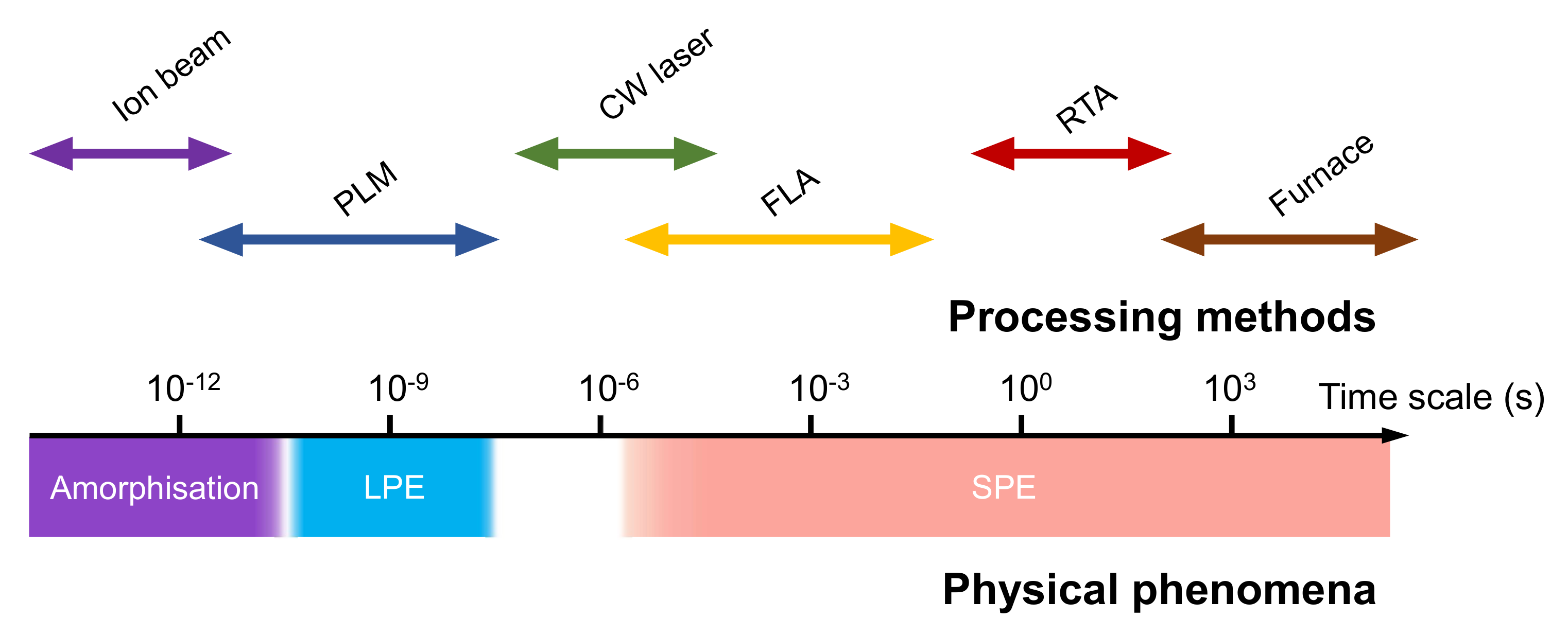
Although both intrinsic defects and extrinsic impurities can be introduced into the Si lattice during wafer growth processes, it is more practical and controllable to introduce them during subsequent processing steps involving but not limited to ion implantation, charged particle or ionising irradiation, and pulsed-laser annealing/melting. Introducing defects or impurity atoms into Si by ion beam irradiation usually requires an annealing (heating) step to remove unwanted damage or recrystallise amorphous layers that can form. The heating can be achieved over many different time scales as illustrated in Figure 1. On the far left of Figure 1 is the typical time scale for individual ions to penetrate and stop in a solid. In Si, this causes defects and amorphisation at sufficiently high ion doses. Conventionally, furnace annealing (shown on the far right of Figure 1) is used to remove or minimise ion-induced defects and to recrystallise amorphous layers by epitaxial growth in the solid phase, or more concisely, solid phase epitaxy (SPE), thus electrically activating (doping) Si with the ion implanted impurities.
Starting in the 1970s, a range of annealing methods emerged that could successfully anneal ion implanted Si. These methods cover a very wide range of time scales and are illustrated in Figure 1. At the longer time scales, above about one microsecond, Si can be crystallised and dopants activated in the solid phase. Shorter annealing times are used to minimise dopant diffusion and other undesirable effects of long annealing times. These more rapid solid phase annealing processes are treated more fully in the following section. At much shorter time scales, less than about a tenth of a microsecond, pulsed lasers can be used to locally melt the near-surface of Si without appreciably heating the underlying solid—we will refer to this process as pulsed laser annealing/melting (PLM). If the laser melts beyond the amorphous-crystalline interface into the underlying crystalline substrate, the molten Si solidifies from the underlying solid by ultra-rapid epitaxial growth in the liquid phase (or, more concisely, liquid phase epitaxy (LPE)), and can lead to high quality monocrystalline Si and dopant activation. If, however, the PLM does not melt beyond the amorphous-crystalline interface, or there is an absence of a substrate seed crystal, subsequent (ultra-rapid) solidification and crystallization will result in polycrystalline-Si (poly-Si) formation. Note that, as compared with LPE during crystal growth from saturated solutions [3], PLM-induced LPE occurs in a localised near-surface layer over much shorter timescales (minutes compared with tens to hundreds of nanoseconds). As outlined below, the ultra-rapid nature of the PLM process has made PLM a particularly attractive method for doping Si with desirable impurities in Si at concentrations well beyond the equilibrium solid solubility limit. In terms of current commercial interest in PLM, it is now a key technique used in the fabrication of commercial flat panel displays (FPD), while current research interest in PLM within the scientific community in to explore the possibility of doping Si with deep level impurities to dramatically enhance near-to-mid-infrared light detection in Si, that is, optical doping.
This article aims to provide a review of both the history and recent studies surrounding the use of PLM (in the nanosecond time scale) for electrical and optical doping of ion implanted Si. Here, electrical doping by PLM involves the incorporation and activation of shallow donor and/or acceptor atoms in the Si lattice for electronic device applications (e.g., when forming pn-junctions). On the other hand, optical doping involves the incorporation and activation of deep level impurities into Si for enhanced sub-bandgap light absorption, which has interesting applications in Si-based near-to-mid infrared light detection. In both these cases, activation of the dopant/impurity atom implies that there is one or more electronic level introduced into the Si bandgap following PLM. However, when activated, the shallow dopants used for electrical doping (i.e., group III and V dopants) introduce donor/acceptor levels in the bandgap that are relatively shallow with respect to the Si band edges (<), whereas deep level impurities used for optical hyperdoping (the chalcogens and transition metals) introduce electronic levels that are deep with respect to the band edges (≫). [1] It is also worth noting that, apart from the chalcogens and transition metals, deep electronic levels (or more succinctly, deep levels) can also be introduced by intrinsic defects in Si, such as those induced by ion implantation [4].
This review will be organised into two major sections, namely electrical and optical doping. Historically, PLM of Si was first pursued to recrystallize ion implanted Si for electrical doping applications, where the initial focus was to electrically activate shallow p- and n-type dopants to achieve charge carrier densities exceeding those possible under equilibrium conditions. Later, it was found that PLM can also be used to crystallise and electrically dope deposited amorphous Si films, which has become the basis for high performance thin film transistor (TFT) fabrication in FPDs. These applications of PLM, as a means of crystallising and electrical doping Si, are discussed in Section 2. On the other hand, Section 3 reviews recent PLM experiments that are focused on optical hyperdoping of Si with deep level impurities for enhanced near-to-mid infrared light absorption. Initial investigations of optical hyperdoping by PLM have been conducted on chalcogen-hyperdoped Si, while more recent experiments have been performed on transition-metal-hyperdoped Si.
2. Electrical Doping of Silicon with Pulsed-Lasers
Laser annealing, or pulsed-laser melting (PLM) as it is now known, was historically applied following ion implantation of suitable impurities as a means of electrically doping Si with conventional group III and V dopants at concentrations far beyond their equilibrium solid solubility limit. These early studies have led to a greater understanding of the trapping and segregation dynamics of the conventional dopants both in solid and liquid phase Si, particularly at short annealing times, and will be reviewed in Section 2.1. Deposited amorphous Si films on Si and other substrates were also investigated under PLM in early studies [5,6]. These studies gave results that are totally consistent with PLM of ion implanted Si (that is, LPE occurred when there was an underlying seed Si crystal and poly-Si resulted when there was an absence of a crystalline seed). Although we do not specifically review here the literature on PLM performed on deposited amorphous Si films, we highlight in Section 2.2 an important thin film application of PLM, specifically, for the fabrication of TFTs in commercial FPDs.
2.1. Historical Overview of Laser Processing (1970s to 1990s): Early Electrical Doping Studies
Major interest in utilising pulsed-lasers for semiconductor processing first emerged in the mid-70s when a group of Soviet scientists demonstrated its effectiveness at removing lattice damage and restoring long-range crystalline order in ion implanted Si and GaAs while simultaneously achieving high levels of electrical doping [7,8]. In contrast, Si lattice damage in the form of dislocation loops and other extended defects were often an unwanted consequence of high dose ion implantation and conventional furnace annealing. Furthermore, as mentioned in the introduction, PLM induces LPE in Si over much shorter time scales (typically in the nanosecond regime) as compared with Si recrystallisation during thermal annealing in the solid phase (millisecond to hours). The short time scale involved in PLM led researchers to believe that PLM could potentially achieve dopant supersaturation in Si at concentrations far beyond levels achievable by solid phase annealing techniques, while at the same time, reducing the concentration of residual defects [8,9].
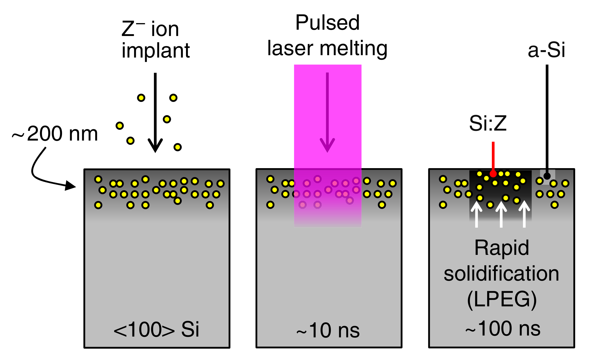
Figure 2 illustrates the ion implantation and PLM processes for electrical and optical doping of Si. Ion implantation generates disorder and amorphisation in the near-surface region where the impurity ions reside. During PLM, an intense pulse of energy is delivered to a localised region on the Si surface, melting it and resulting in a large temperature gradient across the (molten) surface and (solid) substrate. Subsequent recrystallisation of the molten surface occurs by LPE within the next tens to hundreds of nanoseconds, provided that the laser has melted beyond the amorphous-crystalline interface into the underlying substrate. In principle, this allows the ion implanted impurities to be “frozen into” the Si lattice at concentrations far beyond the equilibrium solid solubility. The resulting material is often referred to as impurity-supersaturated Si or impurity-hyperdoped Si in the literature. However, for the purpose of our discussion in this review, we will make a distinction between the two terminologies as follows: supersaturation will simply refer to the situation when the soluble impurity concentration exceeds the equilibrium solid solubility by about an order of magnitude or more, while hyperdoping refers to exceeding equilibrium solubility by at least several orders of magnitude as well as providing a similarly high level of electrical or optical activity of the introduced impurity. Note that successful LPE from PLM generally depends on the specific laser conditions such as the laser wavelength, energy density and pulse duration, as well as the implantation parameters prior to PLM. Readers are also referred to Ref. [9] for a more comprehensive and in-depth discussion about the physical processes involved during PLM.
In the initial ion implantation and PLM experiments in the late 1970s and early 1980s, electrical measurements and structural characterisation of Si implanted with various group III and group V dopants were very promising [8,9,11,12,13,14]. Soluble dopant concentrations beyond the equilibrium solid solubility limit were achieved for P, B, As, Sb, In, Ga and Bi (see Table 1). For B, P and As, practically all of the implanted atoms were electrically activated with little to no surface segregation during LPE. On the other hand, differing degrees of surface segregation were observed for Sb, In, Ga, and Bi (and in some cases, surface loss) as a consequence of their much lower equilibrium solid solubilities as compared with B, P and As [13,15,16]. Note that significant dopant diffusion can occur within the molten surface layer, thus broadening the ion implanted profile. Transmission electron microscopy (TEM) and Rutherford backscattering spectrometry with channeling (RBS-C) measurements confirmed that all of these ion implanted and PLM-processed samples were free from macroscopic defects when the implanted dose was kept below around (specific dose depended on the dopant species). Above this implantation dose, defective epitaxy was observed following PLM [9,17,18,19]. Note also that microscopic vacancy complexes smaller than the resolution of TEM (< 10 Å) were subsequently reported from deep level transient spectroscopy (DLTS) measurements in PLM-processed Si (even without the prior implantation step) [8,20]. Both the defective epitaxy concentration regime and the presence of PLM-induced microscopic defects will be discussed in later sections of this review.
The strong interest in using pulsed-lasers to anneal ion implanted Si in these early studies stimulated interest in the possibility of using continuous wave (CW) lasers [21,22,23,24,25]. In these cases, the heating time scale was around the s to s (see Figure 1). Similar to PLM, there is a strong temperature gradient during CW-laser annealing that decreases from the surface, with the surface temperature somewhat below the Si melting point. It was found that implantation disorder could be effectively removed using CW-laser annealing. Furthermore, recrystallisation occurred in the solid phase and active dopant concentrations somewhat exceeding the solubility limit could be achieved. The effectiveness of this rapid and selective annealing by CW-lasers made it possible to effectively activate ion implanted dopants with minimal diffusion, while keeping the underlying substrate at lower temperatures.
In terms of effective annealing of ion implantation damage, dopant solubility and activation, these early studies, in turn, stimulated much interest over the 1980s and early 1990s in examining a range of other rapid annealing methods that straddled the timescales between CW-lasers and conventional furnace annealing [25,26]. These methods are also illustrated in Figure 1 and include various forms of flash lamp annealing (FLA) [26,27,28] and rapid thermal annealing (RTA) [29,30,31,32]). They are also capable of achieving effective crystallisation and defect removal in the solid phase, with minimal dopant diffusion similar to the CW-laser case, as well as dopant solubilities exceeding equilibrium values. However, more detailed studies of dopant solubility following furnace annealing over much longer time scales found similarly high levels of dopant supersaturation at moderate temperatures between 500 °C to 650 °C [33,34,35].
Once it was realised that effective annealing of ion implanted Si could be carried out over a wide range of time scales, there was an effort to explore the particular advantages of each method. One important issue was the degree of dopant supersaturation and whether that could lead to correspondingly high electrically active concentrations that were stable under normal device operating conditions. A summary of the maximum level of dopant supersaturation and measured electrical activity that can be achieved using PLM and RTA/furnace annealing for P, B, As, Sb In, Ga and Bi is given in Table 1. Note that, in all cases, supersaturation can be achieved but subsequent furnace annealing at elevated temperatures (900 °C to 1100 °C) resulted in a return to equilibrium conditions, that is, significant precipitation of the supersaturated dopants, long range diffusion, and, in some cases, dopant segregation to the surface [9,35,36]. In other words, supersaturated dopant concentrations are thermally metastable.

Table 1.
Maximum equilibrium solid solubility () of various group III and V dopants in Si (obtained from Ref. [16]) and their highest experimentally observed metastable solubility in <100> Si from ion implantation followed by either solid phase annealing (furnace annealing or rapid thermal annealing, represented by and , respectively) or liquid phase PLM. Maximum carrier density measurements when available are reported in brackets. All values are reported in units of cm.
| P | B | As | Sb | In | Ga | Bi | |
|---|---|---|---|---|---|---|---|
| [15] | |||||||
| PLM | 5- | 5- | |||||
| (5-) | () | (5-) | () | [15] | [15] | [15] | |
| [12,17,37] | [11,17,37] | [15,17,37] | [15,38] | ||||
| Furnace | - | 1.3- | 5.0- | 4.0- | |||
| annealing | [31] | [33] | () | [33,34,39] | [39] | [35,39] | |
| and RTA | () | () | [33,34,39,40] | () | |||
| [41] | [31] | [28] | [39,42] |
As discussed above, both solid phase and liquid phase annealing methods, under suitable conditions, can result in substantial dopant supersaturation well beyond the solid solubility limit without apparent phase separation or precipitation. However, this situation does not necessarily imply correspondingly high levels of electrical activity. For example, some dopant atoms may not be located on electrically active lattice positions. They may form dimers, trimers or small clusters, and they may also form complexes with defects such as vacancies [32,43], which, depending on the specific nature of the defect complex, may or may not be electrically active. In such cases, the ‘active’ dopant concentration may be slightly or significantly below the apparent ’soluble’ impurity concentration (also see Refs. [40,44,45]). Indeed, as shown in Table 1, following annealing in the solid phase over a wide range of time scales (furnace and RTA), the measured charge carrier density is always lower than the measured level of maximum supersaturation, with the exception of B. Similar observations were also made in FLA-processed samples, although these are not specifically included in Table 1 (see instead Refs. [28,46]). Note also that, with the solid phase annealing methods, the difference between the maximum supersaturation and maximum electrical activity depends on the dopant. For example, in the case of Sb, the maximum electrical activity is only slightly below the maximum solubility, whereas for As there is almost an order of magnitude difference [32,40,44,45]. Reports show that, for B, P, As and Sb, the maximum electrically active concentrations appear to be ‘pinned’ at a level at or just below . Interestingly, electrically active concentrations above the observed level of supersaturation have also been reported for B in Si from both solid and liquid phase annealing [11,46]. This suggests that defects or defect-B complexes may also be electrically active, making it difficult to estimate the degree of specific dopant solubility.
Following the more extensive rapid solid phase annealing studies of ion implanted Si in the 1980s as outlined above, the initial excitement for the potential of PLM for Si device fabrication waned considerably. Indeed, from a device perspective, the advantages of solid phase RTA (and FLA) were compelling in comparison with PLM. For example, electrically active dopant concentrations were comparable across rapid SPE and PLM (as shown in Table 1), and residual defect, dopant profiles and reduced diffusion could be accurately modelled and simulated under short solid phase annealing regimes. In addition, RTA could be easily integrated into device fabrication infrastructure and process lines at the time. Hence, there was little motivation at the end of the 1980s to further explore PLM for electrical activation of dopants and other applications in device processing. This has been largely the case up to the present time, with some notable exceptions, such as for flat panel display processing, as discussed in the following section. In terms of optical doping, there was little if any interest in exploring PLM in this regard during early laser annealing studies. However, PLM of several transition metal elements implanted into Si was examined during this time [9,47,48] and these early studies provided stimulus for later studies as is outlined in Section 3.2 below.
To summarise this section, initial PLM studies were mostly systematic surveys performed on the group III and V dopants in Si. These experiments demonstrated the possibility of using PLM for dopant activation at concentrations beyond the solid solubility limit, but it was subsequently found that similar solubilities and electrical activities could be obtained by solid phase annealing. Hence, there was little motivation from the Si microelectronics device industry to pursue PLM for annealing: rather, RTA (and later FLA) in the solid phase was embraced. As we indicate below, the major continued interest in PLM has been for fabricating FPDs and for optical doping.
2.2. Electrical Doping by Plm beyond the 1990s: Flat Panel Displays
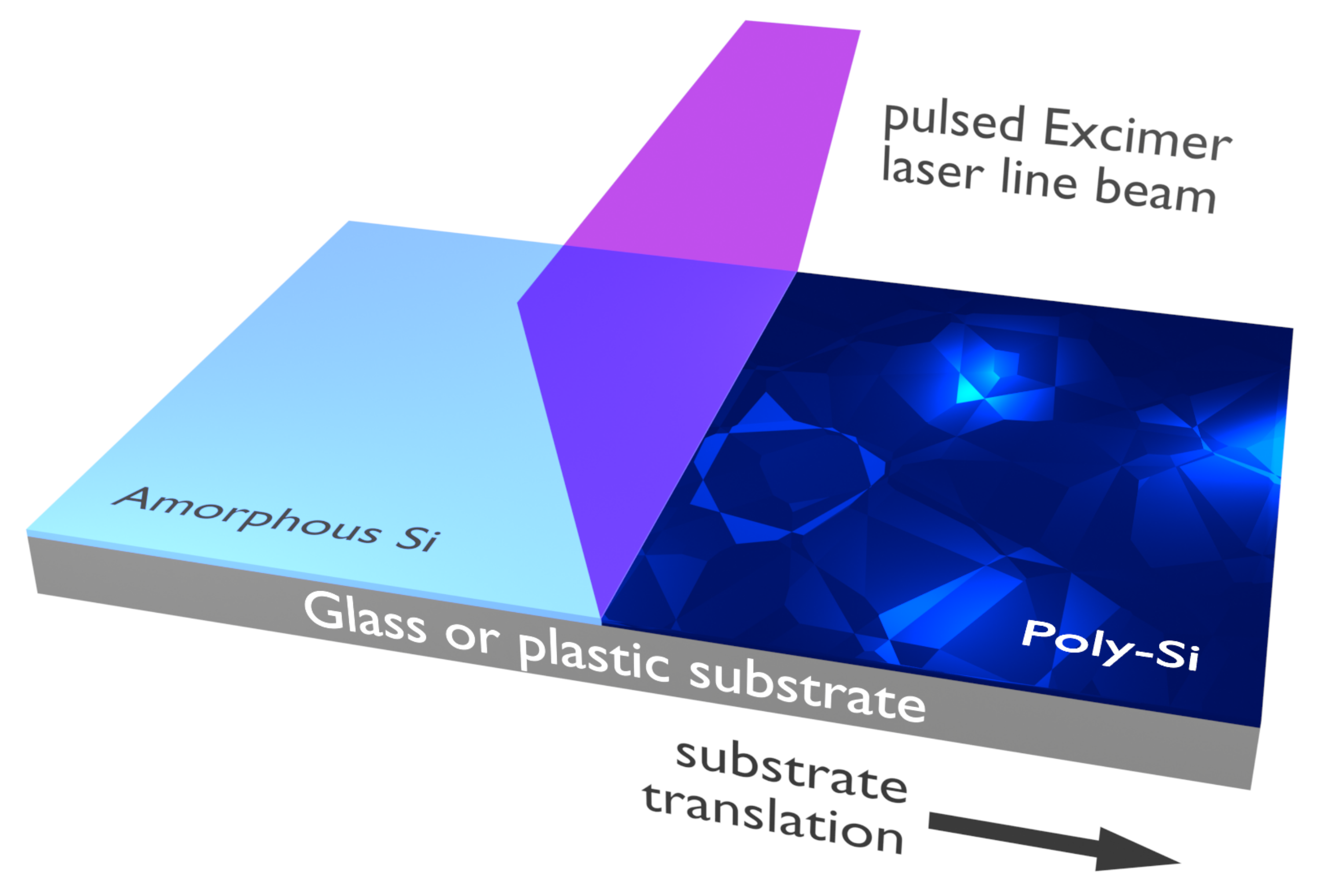
A major application of PLM in optoelectronics is for the crystallisation of thin films of deposited amorphous Si in FPDs. To achieve the required electrical doping and to increase carrier mobility, crystallisation of these deposited thin films of amorphous Si is highly desirable but, since the substrate in FPDs is either glass or a plastic material, solid phase crystallisation at temperatures of 650 °C is not possible without far exceeding the softening point of the substrate. PLM was investigated in the early to mid-1990s as an attractive way to overcome this problem and to provide poly-Si thin films with excellent electrical properties [49,50,51,52,53]. Both active matrix liquid crystal displays (AMLCD) and active matrix organic light emitting diode (AMOLED) displays require an active backplane containing TFTs and associated circuitry that defines the pixelation of the display. For high resolution FPDs, the footprint of each TFT needs to be as small as possible, which requires optimised electrical properties such as high electrical doping and electron mobility. Hence, conversion of deposited thin film amorphous Si into reasonably large grain poly-Si is desirable.
PLM was specifically developed for this FPD application [52] and the typical PLM arrangement that has been used is shown in Figure 3. Lasers operating at short UV wavelengths, such as XeCl Excimer lasers, ensure that laser light is absorbed in the near-surface of the Si thin film. In addition, a short pulse length of a few nanoseconds ensures that the amorphous Si can be melted with little temperature change to the underlying glass or plastic substrate. It is important to emphasise that, since there is an absence of a seed crystal, ultra-rapid solidification following PLM results in poly-Si. For melting large areas, such as in FPD panels, the output of the laser is first homogenized and then formed into a narrow line beam. Following deposition of a thin amorphous Si film, the substrate is usually scanned across the beam, while the laser is repetitively pulsed. Typically, the substrate translation rate is synchronized with the laser repetition rate to ensure that each area of the amorphous Si film is irradiated with sufficient energy to completely melt through the Si film (around 50 nm in thickness) during a single pass of the FPD panel. Under optimum conditions, the underlying glass or plastic substrate remains significantly below 100 °C [52], and thus there is no significant degradation of the substrate during PLM to form poly-Si.
3. Optical Hyperdoping with Deep Level Impurities
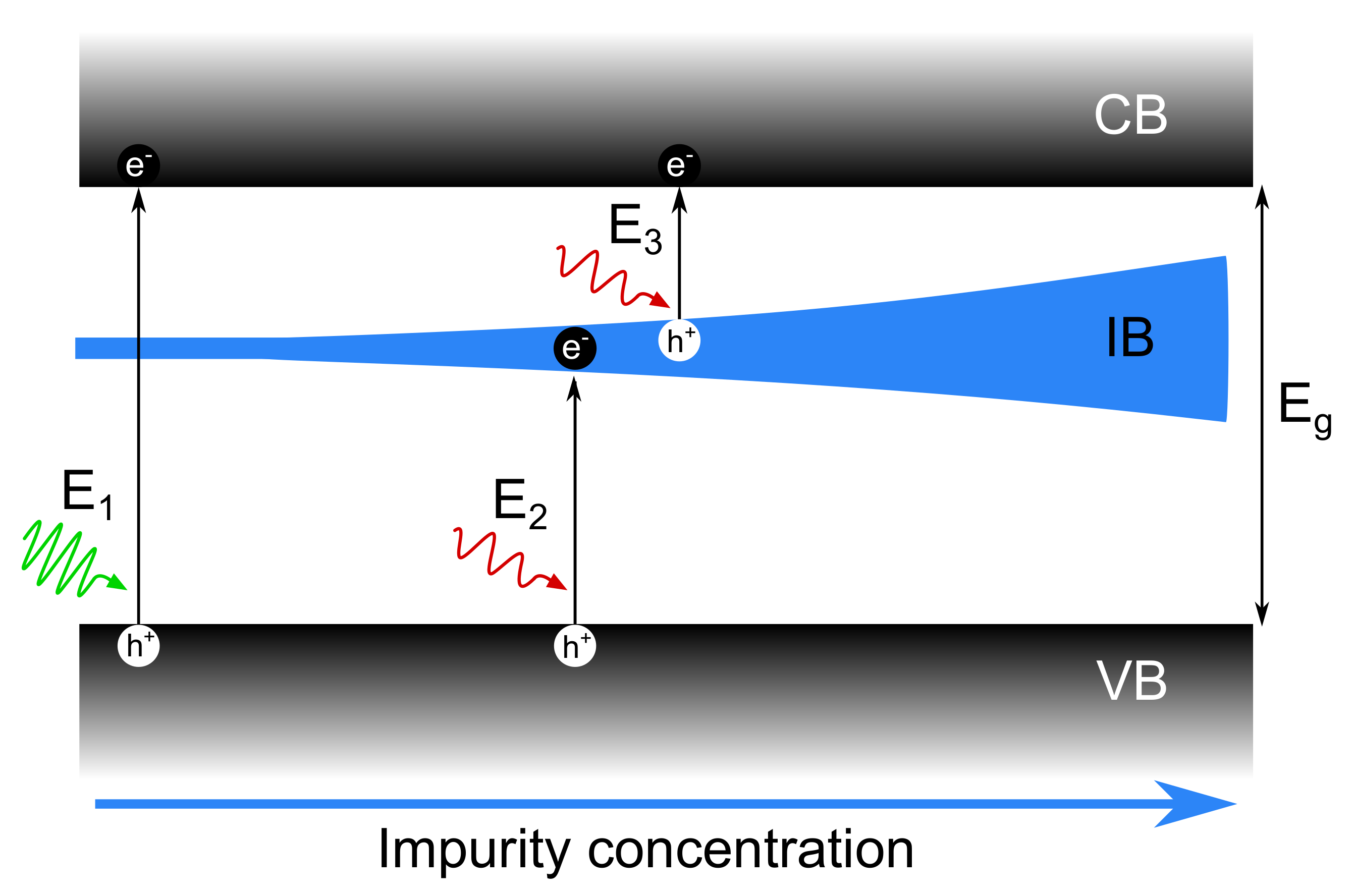
As discussed in Section 2.1, although PLM has shown promise in terms of highly effective electrical doping and removal of ion implantation damage in Si, similar outcomes could also be achieved by solid phase annealing techniques that are more cost-effective. Thus, there was little to no incentive in pursuing further research for the purposes of electrical doping in Si by PLM. Rather, continued experimental interest in PLM since the late 1990s has been for the optical doping of Si with deep level impurities such as the chalcogens (S, Se, Te) and transition metals, which has provided further insight into the importance of impurity diffusion and solubility (both in the liquid and solid) to the overall doping behaviour of these impurities in Si. In contrast to the shallow group III and V dopants, deep level impurities introduce electronic levels deep in the Si bandgap, enabling near-to-mid infrared sub-bandgap optical excitations. As illustrated in Figure 4, when deep level impurities are introduced into Si at sufficiently high concentrations ( cm), they can, in principle, result in an intermediate band (IB) in the bandgap and hence achieve efficient sub-bandgap optical absorption [1,54]. Furthermore, it has been proposed that the formation of an IB can also result in improved carrier transport properties as compared with discrete impurity levels [55]. The favourable optical and electrical properties of IB semiconductors has motivated researchers to physically realise such material systems through various methods [56,57], one of which is by hyperdoping Si with deep level impurities, which has attractive applications as Si-based infrared optoelectronic devices (e.g., telecom band detectors and IB solar cells) [1,54,58].
Since the required level of hyperdoping is generally several orders of magnitude greater than the equilibrium solid solubility of deep level impurities in Si, nanosecond scale PLM became a logical candidate for fabricating such materials. Early Si optical hyperdoping experiments involved the use of multiple PLM pulses both in the femtosecond and nanosecond timescales, and these studies were performed in an atmosphere [59,60]. However, in addition to achieving appropriate levels of sulfur-hyperdoping, femtosecond-PLM also introduces surface microtextures that are known to significantly reduce the reflectivity of Si [61,62]. Subsequent chalcogen-hyperdoping experiments focused on using ion implantation followed by a single ns-PLM pulse to achieve greater control over the impurity profile and concentration, while also avoiding surface complications introduced from fs-PLM [63,64,65].
3.1. Chalcogen-Hyperdoped Silicon
Physical, electrical and optical measurements (TEM, electron diffraction, RBS-C, secondary ion mass spectrometry (SIMS), resistivity, optical absorption) showed significant promise in terms of the successful hyperdoping of S, Se and Te impurities in high quality single crystalline Si from ion implantation followed by ns-PLM [63,64,65,66,67]. Specifically, S, Se and Te concentrations up to were achieved in the chalcogen-hyperdoped Si layer, with an estimated average carrier density of around . These chalcogen-hyperdoped Si materials also demonstrated significant enhancements in the sub-bandgap optical absorption up to mid-infrared wavelengths (2.5 m) with little diminished absorption at the longer wavelengths. These results have been summarised in a recent review on the topic in Ref. [54].
The high levels of chalcogen-hyperdoping and sub-bandgap absorption led the authors to believe that a chalcogen-induced IB had formed in their samples. However, there were several peculiarities observed in the optical and electrical measurements that could not be explained by the presence of a chalcogen-induced IB alone. Firstly, the absorption coefficient increased with decreasing photon energy below 0.2 eV. In addition, the photoresponse of fabricated junction detectors was limited by very large reverse leakage currents () despite being strongly rectifying [64]. These detectors were also reported to have abnormally large current gains that did not appear to obey conventional photocurrent gain mechanisms such as avalanche gain and photoconductive gain [66].
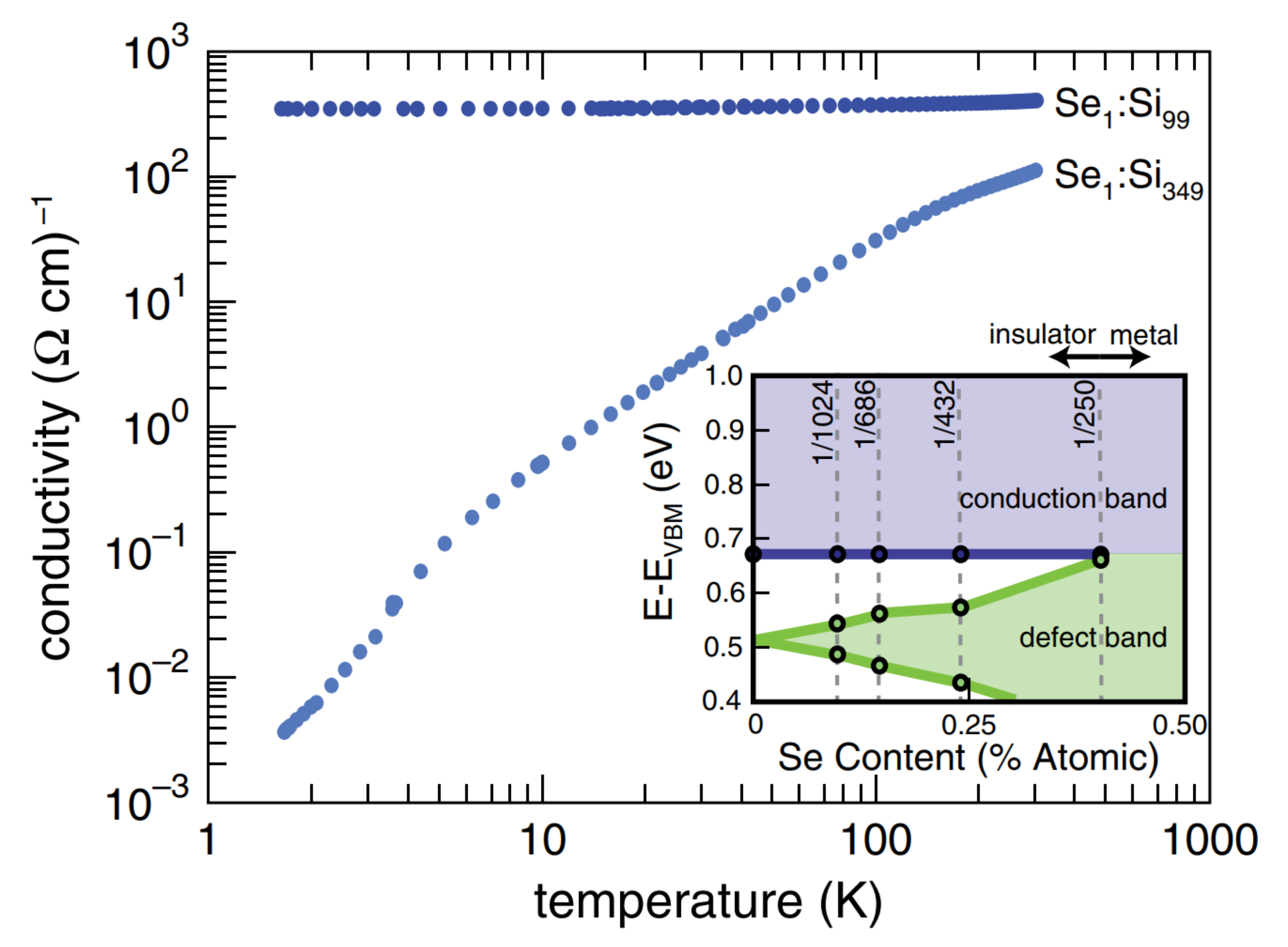
It was later revealed that some of these observed anomalies were most likely caused by an insulator-to-metal transition (IMT) at room temperature. Temperature-dependent conductivity measurements performed on S- and Se-hypedoped Si confirmed that the samples were metallic/degenerate at sufficiently high impurity concentrations [68,69]. A representative conductivity-temperature plot is shown in Figure 5. Since the double donor levels of S and Se are only about 0.1 eV to 0.3 eV from the CB edge (likely the same for Te), as the chalcogen impurity concentration increases, the IB widens and eventually overlaps with the CB, as illustrated in the inset of Figure 5. Thus, rather than introducing an IB, the bandgap of Si is effectively narrowed. Furthermore, since chalcogens are double donors, the merged IB/CB will be heavily populated by electrons such that the Fermi level is positioned within the merged IB/CB, rendering it degenerate. In addition to metallic conductivities, such an IMT could also give rise to the observed long wavelength MIR absorption (from free carrier absorption within the merged IB/CB, and not sub-bandgap processes), as well as large reverse leakage currents in fabricated junction diodes.
To counteract the effects of an IMT, Simmons et al. [70] employed a dopant compensation technique by co-doping sulfur-hyperdoped Si with B in an attempt to control and lower the position of the Fermi level by fine tuning the acceptor-to-donor ratio. These efforts successfully reduced the electron density in the CB and resulted in a three orders of magnitude improvement in the 1550 nm photoresponse when the Fermi level was lowered to just below the bottom edge of the IB (achieved when the B and S concentrations were matched).
Nevertheless, the relative shallowness of the double donor levels introduced by chalcogens in Si has unfortunately limited the potential of chalcogen-hyperdoped Si as an IB semiconductor and an efficient infrared photodetector. Although dopant compensation techniques have shown promise, they require meticulous fine tuning of the co-dopant profile and concentration to match that of the chalcogen impurity. Research efforts have since shifted gears towards impurities that introduce much deeper intermediate levels in the Si bandgap (i.e., closer to mid-gap), such as the transition metals.
3.2. Transition-Metal-Hyperdoped Silicon
This subsection will first treat measurements of the physical and structural aspects of transition-metal-hyperdoped Si using PLM, and then cover the optical and photodevice characterisation. The reason for this ordering is that it is essential to first understand the physical nature of transition-metal-hyperdoped Si, before interpreting the optical and photodevice measurements.
3.2.1. Physical and Structural Characterisation
Unlike the chalcogens, transition metals have much higher diffusivities ( to ) compared to the chalcogens ( to ), in addition to their low solubilities in solid Si. The equilibrium solid solubility of most transition metals in Si is around at 1300 °C, which is still three to four orders of magnitude lower than the critical concentration required for IB formation in Si. As a result, even with PLM, it has been significantly more challenging to obtain the hyperdoping concentrations necessary for IB formation with transition metals.
Recht et al. [71] performed a systematic survey that investigated the physical behaviour of various transition metal impurities implanted in Si under ns-PLM, including Au, Co, Cr, Cu, Fe, W, Zn, Pd and Pt. Several important observations resulted. First, the authors found that both the diffusivity of the metal species at the melting temperature, , and the equilibrium partition coefficient, (equilibrium concentration ratio of the impurity across the solid-liquid interface), affect the diffusion velocity of the metal species in molten Si. Due to much lower solubility in the solid, impurity supersaturation in the solid can only be achieved if the solid-liquid interface velocity during Si solidification outruns impurity diffusion in the melt towards the surface. The interfacial velocity can be controlled through the specific PLM parameters (laser wavelength, pulse duration, energy density). Hence it should, in principle, be possible to obtain supersaturation in the solid under suitable PLM conditions. Indeed, Recht et al. [71] were able to demonstrate some degree of success with Au and Zn. Even in these two cases, however, supersaturation was accompanied by strong impurity segregation, both laterally and towards the surface, as will be discussed below.
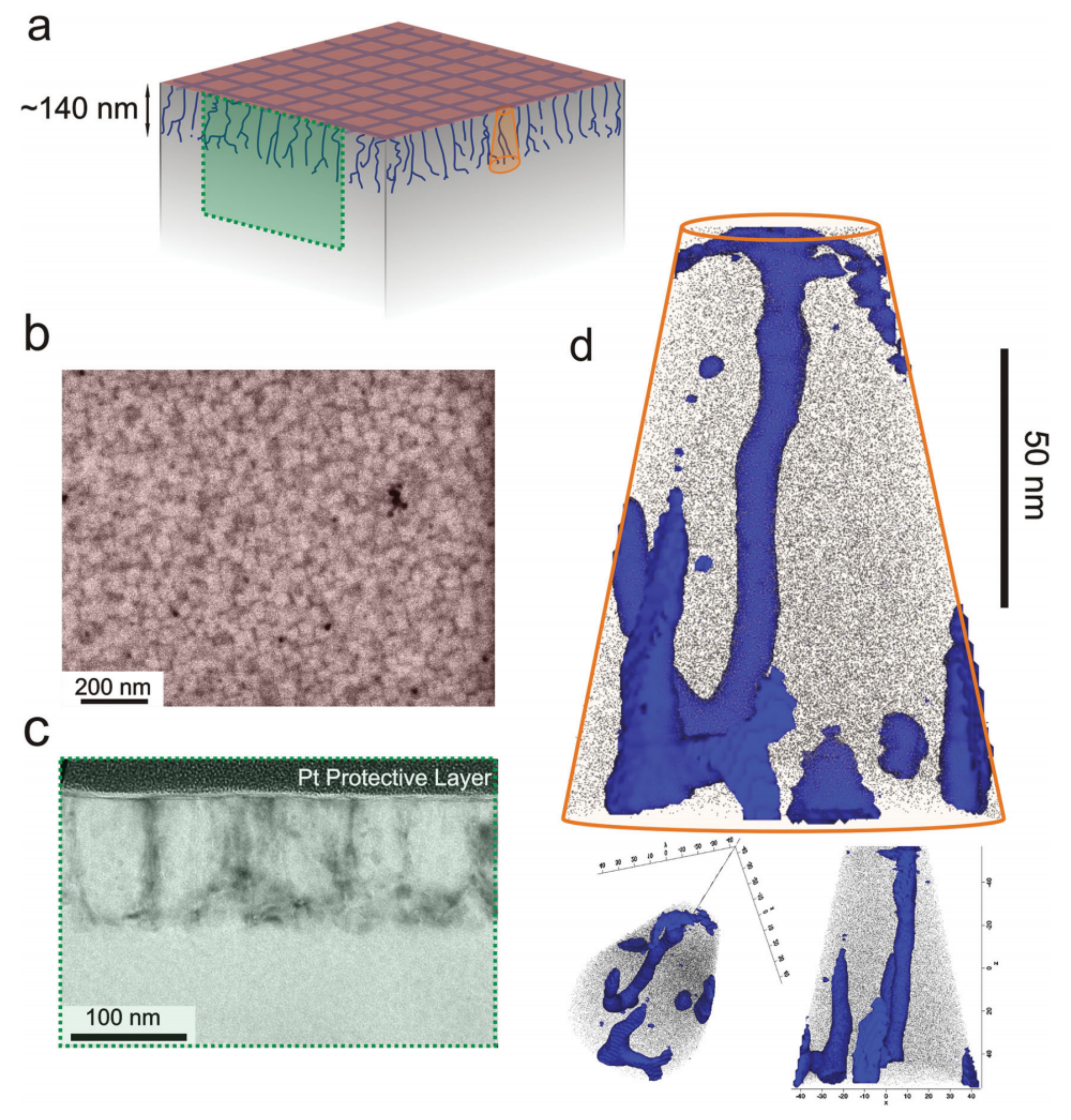
For most of the transition metal impurities studied, lateral and surface segregation appeared to dominate during LPE, with insignificant quantities of the impurity species remaining in solid solution in Si. An example of the latter observation is atom probe tomography (APT) measurements performed on Co implanted Si followed by PLM [72]. A summary of these results is provided as Figure 6. Briefly, APT revealed that practically all of the Co atoms reside on the surface or within vertical columnar structures referred to as filaments (blue structures in Figure 6d) that extend from the surface. These filaments are a result of lateral Co segregation during LPE, with insignificant amounts of Co (at least in terms of hyperdoping) in the single crystalline Si regions between them. Note that this lateral segregation phenomenon at high impurity concentrations under LPE is not unusual, and has previously been reported in early Si PLM studies involving a wide range of metal impurities (Cu, Fe, Zn, Mn, W, Mg and Cr) [9], as well as in more recent optical hyperdoping experiments involving Ti, V and Ag [73,74,75,76,77,78,79]. In some of these earlier experiments, the PLM samples were characterised by TEM which often did not contain the same high spatial and concentration resolution as APT. The lateral segregation of impurities in these transition metal studies was thought to be related to so-called cellular breakdown that was previously observed in Si supersaturated with group III and V dopants following implantation and PLM. Nonetheless, regardless of whether lateral impurity segregation results in near-equilibrium cellular breakdown or in far-from-equilibrium filamentary behaviour, both phenomena give rise to defective epitaxy following PLM and little impurity is trapped in good quality crystal between the cells/filaments.
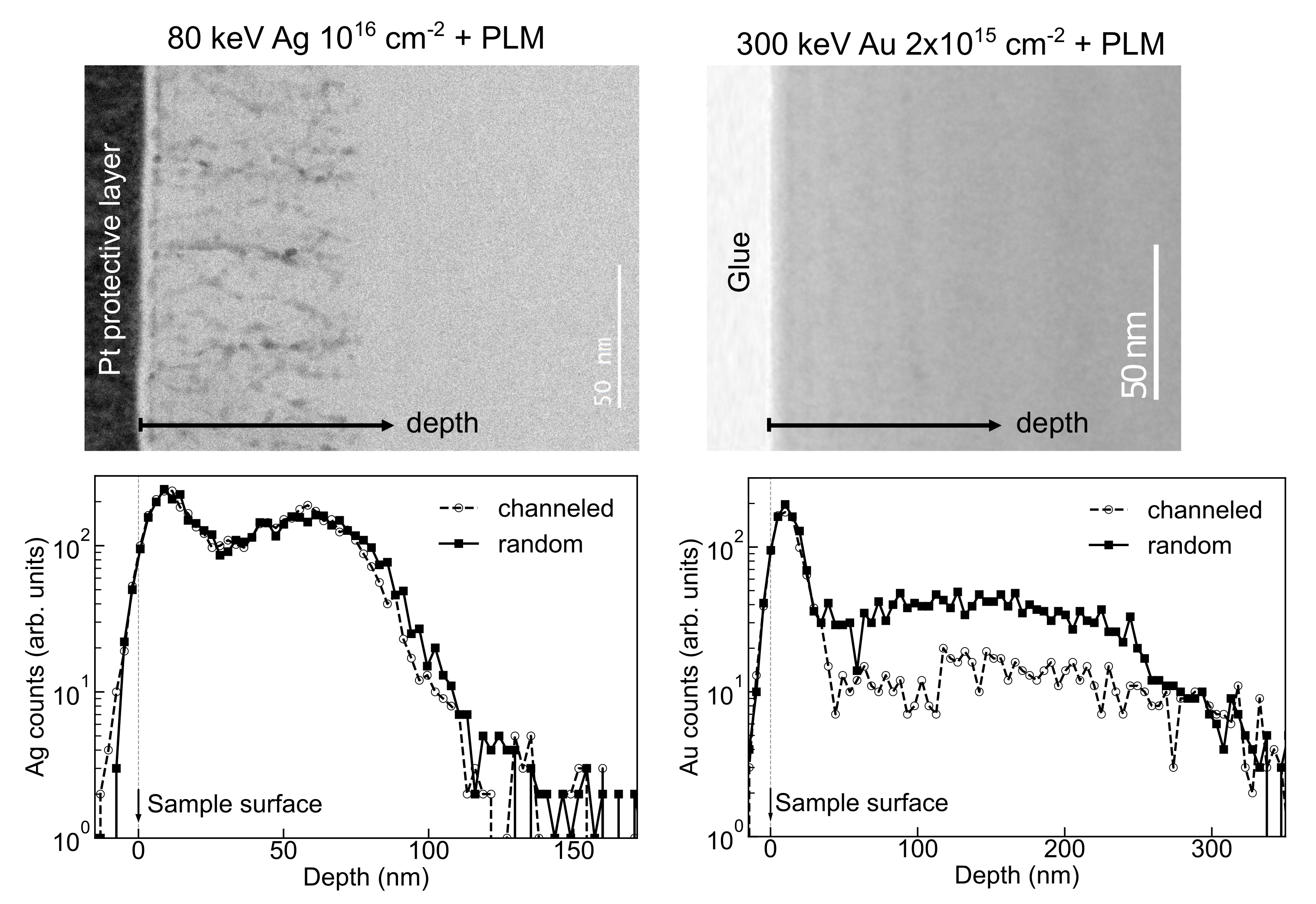
Further insights into the complex impurity redistribution processes involved during LPE have been provided in a very recent study by Lim et al. [79] These authors suggested that, for impurities such as Ag and Ti, there does not appear to be a suitable set of implantation and PLM conditions that will result in homogenous supersaturation (and hence hyperdoping) of these impurities in monocrystalline Si. In particular, below a certain threshold implantation dose unique to the particular metal species and implantation energy, PLM resulted in complete impurity segregation to the surface; while above this threshold implantation dose, highly defective epitaxy was observed due to the strong lateral segregation of impurities associated with filamentary breakdown. Representative TEM and RBS-C data for Ag implanted Si followed by PLM, illustrating both surface and lateral segregation phenomena are shown in the left panel of Figure 7. Note that the subsurface Ag peak in the Ag profile is due to lateral segregation of Ag into filamentary structures and not from homogenous impurity supersaturation, as has been verified by APT (see Ref. [79] for further details). This behaviour is very similar to the Co measurements shown previously in Figure 6d. In other words, practically all of the Ag (and Ti [75,77]) atoms appear to be confined either within the filamentary structures or on the surface.
Despite the apparent difficulty in hyperdoping almost all transition metals homogeneously in monocrystalline Si, Au is a particular exception. Successful Au-supersaturation at a level similar to the critical concentration required to form an IB was first demonstrated by Priolo et al. [47] (1988), and more recently, with optical hyperdoping in mind, by Mailoa et al. [10] (2014) who used ion implantation (50 keV, various Au doses) and ns-PLM (355 nm Nd:YAG, 5 ns, ). Subsequent RBS-C and angular scan measurements [80] provided further insights into the specific Au atom location in the recrystallised Si lattice. As shown in the right panel of Figure 7, there is significant Au supersaturation underneath the thin surface segregated Au layer and more than 90% of this supersaturated Au is located on substitutional lattice sites following PLM. Note that the substitutional Au fraction can be found using the difference between the random and channeled spectra for Au [80]. Importantly, there is sufficient substitutional Au for IB formation, noting that the two well known Au deep donor and acceptor levels in Si are introduced by substitutional Au [81,82]. (Not all substitutional configurations of transition metals are electrically active. For example, Ti deep levels in Si are introduced by interstitial Ti [81,83]. In the context of hyperdoping for IB formation, high concentrations of electrically active deep levels are required. For Au and Ag, these are the substitutional lattice configurations while for Ti it is the interstitial. Readers are referred to Ref. [79] for a more detailed discussion.) Similar results have also been reported in Au-hyperdoped Si fabricated from depositing a 1 nm thin film of Au on monocrystalline Si followed by ns-PLM [84].
Additionally, Yang et al. [80] have also shown that high quality Au-hyperdoped Si can be achieved with higher Au implantation energies up to and exceeding 300 keV, followed by PLM. This effectively increases the thickness of the Au-hyperdoped Si layer and the absorption depth of related sub-bandgap photons. Furthermore, the total substitutional Au content also increases with increasing implantation energy and dose. As will be shown in the following section, these improvements have led to further enhancements in the overall sub-bandgap optical absorption which should, in principle, translate to improved infrared light detection efficiencies of fabricated detectors.
3.2.2. Optical and Photodevice Characterisation
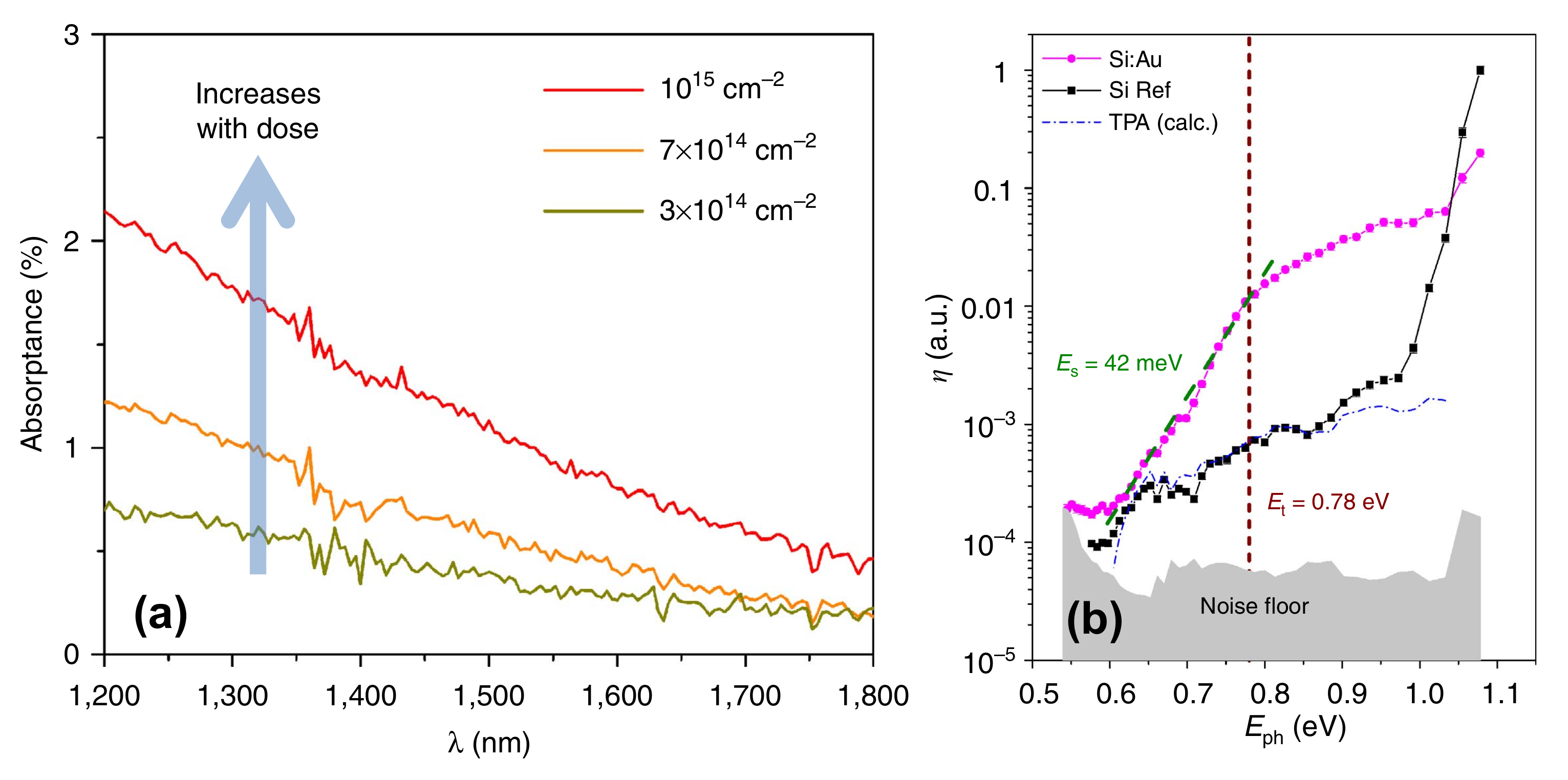
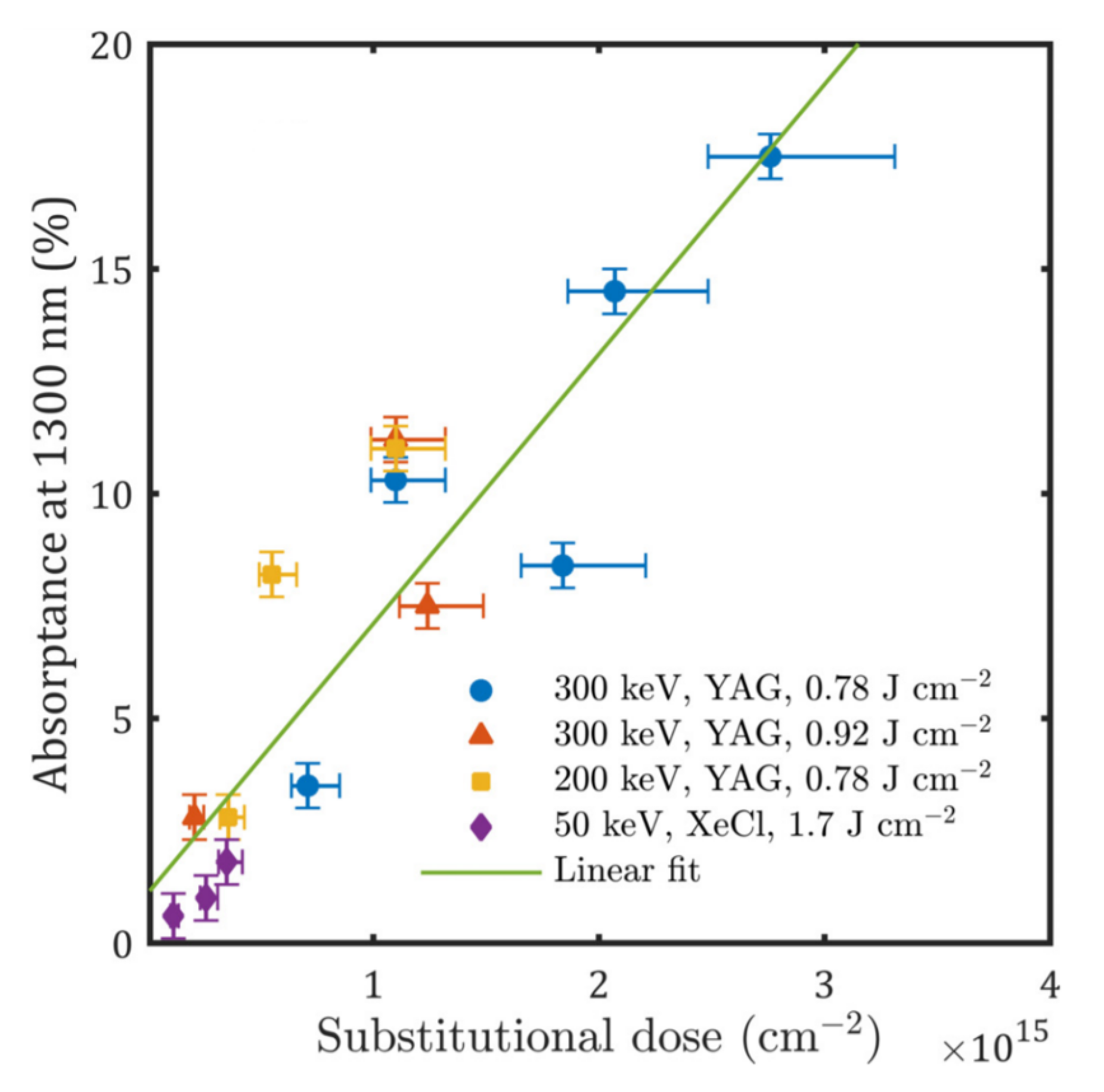
Having established strong evidence for Au-hyperdoping in Si in the above subsection, we now consider corresponding optical and device characteristics. Figure 8 shows the sub-bandgap absorption and photoresponse of Au-hyperdoped Si from Ref. [10]. It is clear from (a) that these Au-hyperdoped Si samples exhibit sub-bandgap absorption that increases monotonically with increasing Au dose (concentration). Furthermore, as shown in (b), enhanced sub-bandgap photoresponse in the NIR was observed in fabricated junction photodetectors, with an activation energy of 0.78 eV. This activation energy was interpreted as evidence for successful Au-hyperdoping, or, in other words, due to the Au deep donor level positioned at 0.78 eV below the CB edge and/or its associated IB. This interpretation was supported by subsequent RBS-C measurements and annealing experiments by Yang et al. [80] who demonstrated a strong correlation between the sub-bandgap absorption and the amount of substitutional Au. A summary of these results is shown in Figure 9. Briefly, the sub-bandgap absorption at 1300 nm is shown to increase linearly with the substitutional Au dose. Note that higher substitutional Au doses were achieved by systematically increasing the implantation dose and/or energy (see Ref. [80] for details). However, as expected, subsequent annealing at moderate temperatures resulted in a noticeable reduction in the sub-bandgap absorption due to Au moving off substitutional lattice sites where they are no longer electrically active [85].
In short, the results above strongly indicate that substitutional Au plays an important role in promoting NIR absorption and photoresponse in Au-hyperdoped Si. However, in the absorption spectra shown in Figure 8a, the spectral lineshape appears to be relatively featureless across the observed spectral range. In particular, if a Au-induced IB has formed from PLM, one might expect a distinct (broad) absorption peak at the optical transition energy between the IB and the CB (approximately 0.78 eV or 1590 nm), as will become apparent below. Furthermore, despite being free from macroscopic extended defects, these Au-hyperdoped Si photodetectors displayed extremely poor external quantum efficiencies (EQE, around at 1550 nm). Similarly, low EQEs were also reported in photodetectors fabricated from Au thin film deposition followed by PLM [84]. The reasons for these peculiarities remained elusive until recently.
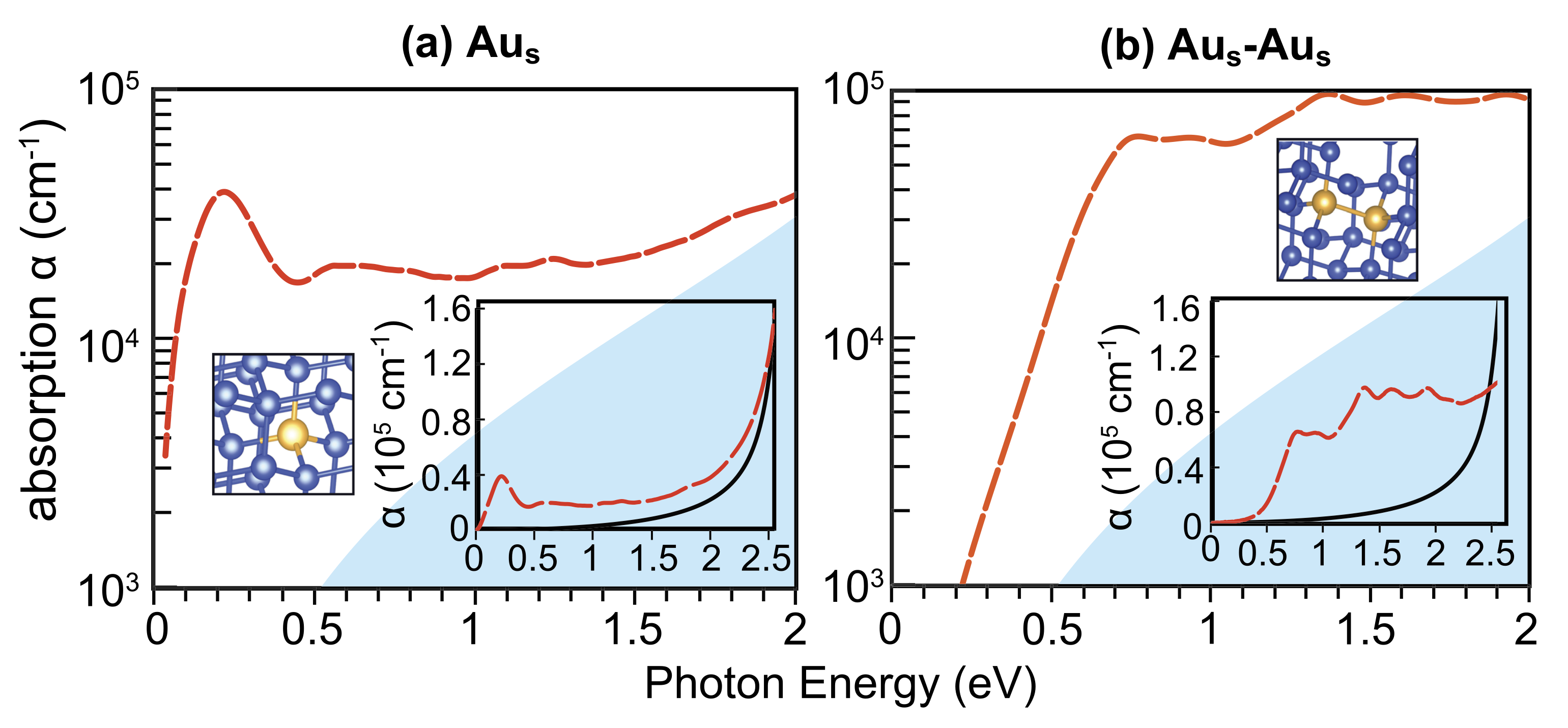
Several publications in recent years have provided valuable new insights into the reason for the apparent anomalies indicated above, as we will now discuss. First-principles density functional theory (DFT) calculations suggest that Au-hyperdoped Si containing approximately purely substitutional Au monomers should, in principle, result in a prominent sub-bandgap absorption peak at the optical transition energy as shown in Figure 10a [82]. Additionally, the experimentally observed sub-bandgap absorption appears to be an order of magnitude lower than predicted from DFT. However, DFT also revealed that, in addition to the Au substitutional monomer (), the substitutional dimer () is also an energetically favourable lattice configuration and can thus be expected to be present in significant quantities in Au-hyperdoped Si. However, unlike , the dimer does not introduce deep mid-gap levels in the Si bandgap. Rather, shallower levels are introduced near the CB and VB edges, resulting in greatly suppressed sub-bandgap absorption and a visibly different absorption spectrum as shown in Figure 10b [82]. In other words, the Au substitutional dimer is not optically active.
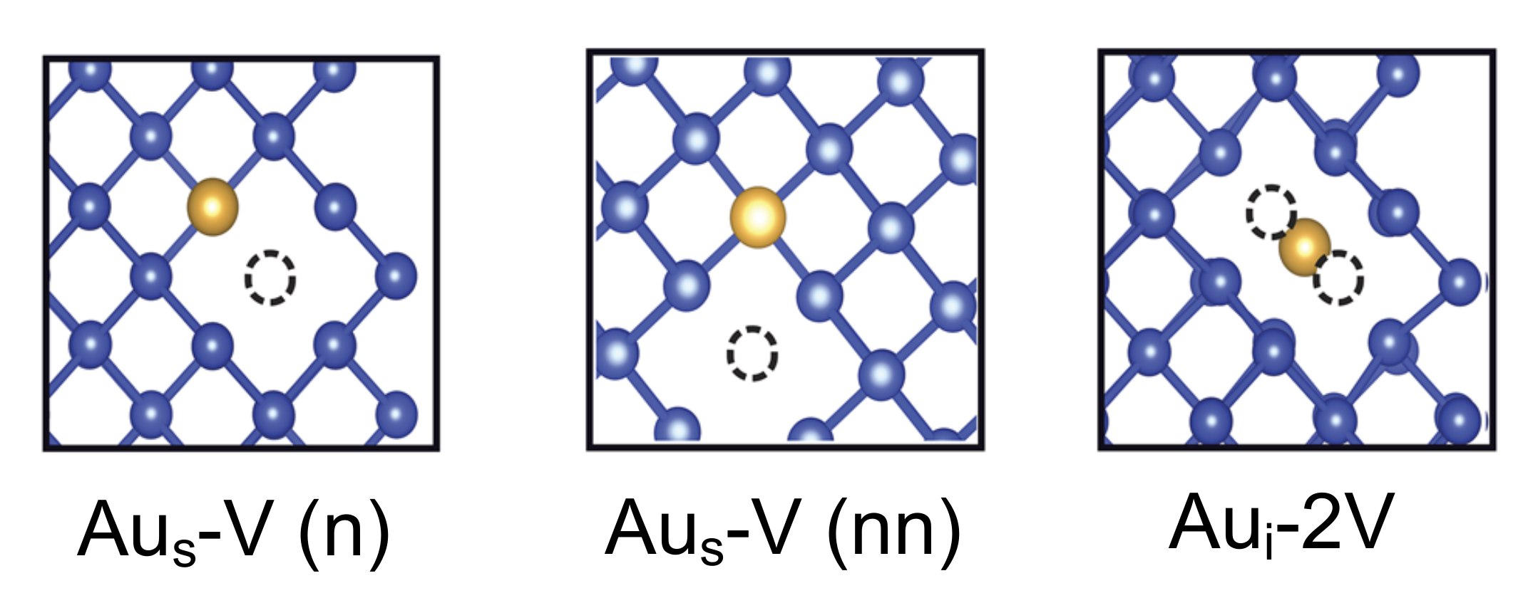
Furthermore, positron annihilation spectroscopy (PAS) measurements indicated that there is an elevated concentration of vacancies trapped along with Au following PLM, presumably to reduce the overall strain in Au-hyperdoped Si [86]. As shown in Figure 11, DFT predicted several Au-vacancy configurations that can form from PLM, and only some of which are optically active. Note that RBS-C cannot distinguish between the , - and various -V lattice configurations.
A major consequence of having a distribution of different substitutional/partly substitutional Au configurations in Au-hyperdoped Si is that the experimentally observed sub-bandgap optical absorption will be greatly suppressed [82,86]. Additionally, since the substitutional Au concentration measured from RBS-C is only about two to three times greater than , it is very likely that there is insufficient optically active Au in the Au-hyperdoped Si samples to form a Au-induced IB. Nevertheless, optically active Au atoms (whether it is or a particular configuration of -V) are still expected to be present at very high concentrations in Au-hyperdoped Si and thus contribute to the sub-bandgap absorption and photoresponse shown above.
In addition to the substitutional Au-vacancy complex, it was recently shown from deep level transient spectroscopy (DLTS) that the implantation and PLM processing introduces microscopic vacancy-type defects that are electrically active [87]. One such defect is the electron trap, , that introduces a deep level at - and is present at concentrations as high as . It is thought to be a vacancy complex extending several hundreds of nanometers away from the implantation end-of-range and the maximum PLM melt depth (i.e., deep in the substrate) and has been suggested to originate from interactions between long range implantation defects (e.g., highly mobile interstitials) and vacancy clusters introduced by PLM. The precise atomic identity and origin of this defect level, however, has yet to be established. Despite showing negligible sub-bandgap optical absorption in comparison with Au-hyperdoping, these process-induced defects were shown to produce a significant photocurrent (under 1550 nm illumination) that approaches the value from optically active Au-related defect complexes (i.e., and some -V) [88]. Indeed, it has been suggested that the kink observed in the spectral response reported by Mailoa et al. [10] and shown in Figure 8, may be a result of this defect (around 0.78 eV above the VB) and not from optically active Au in Si. Nevertheless, the above observations indicate that the photo-generated carrier collection efficiency at the device contacts must be extremely poor to result in the observed EQE values. It has been suggested that the poor carrier collection efficiency is likely due to the short carrier lifetimes within the Au-hyperdoped Si layer, as well as the unoptimised device architecture (vertical and, in some cases, mesa structures) [88]. Improvements to the overall EQE can thus be expected from device architectures that are tailored to the carrier transport properties of Au-hyperdoped Si (e.g., closely spaced planar structures), as well as improving the electrical contact properties. Note that these optimisation strategies to improve the device EQE are in addition to previous efforts that were targeted at increasing the Au-hyperdoped layer thickness (absorption depth) and active Au concentration (absorption coefficient) through optimisation of the implantation energy and dose, as discussed in the previous section.
To summarise this section, Au-hyperdoped Si has been shown to enhance Si sub-bandgap absorption and this method has attractive potential applications as an efficient Si-based infrared photodetector. However, photodetectors fabricated to date have extremely low EQEs that do not appear to be consistent with correspondingly high levels of NIR absorption. Detailed device analysis has revealed that the EQE is limited by the poor photo-carrier collection efficiency at the contacts due to short carrier lifetimes in the Au-hyperdoped Si layer, as well as unoptimised device architectures. Furthermore, DFT calculations and PAS measurements collectively suggested that Au-hyperdoping levels are unlikely to be high enough to result in the formation of a Au-induced IB. In hindsight, even in the absence of an IB, it is very likely that significant improvements to the EQE of Au-hyperdoped Si photodetectors can be achieved from further optimisations to the device architecture (e.g., by introducing waveguides and ring resonators [4]), as well as improved electrical contacts. These introductions should subsequently lead to the commercial realisation of efficient all-Si near-infrared photodetectors based on the introduction of deep levels by implantation of Au.
Beyond Au, there are also numerous publications detailing the optical, electrical and device characteristics of similarly prepared transition metal-doped Si samples [76,78,89,90,91,92,93]. A substantial amount of work was performed on Ti implanted into Si, followed by PLM, and readers are referred to Ref. [1] for a more detailed summary surrounding these results. It is important to reiterate that these Ti samples (as well as others such as V (vanadium) and Ag) are characterised by defective epitaxy due to filamentary breakdown. Nevertheless, these transition metal-doped Si samples exhibited enhanced sub-bandgap absorption in the near-to-mid infrared [78,89]. Although these samples were also characterised by high “metallic-like” conductivities, photoconductivity is most likely caused by a hopping conduction mechanism between impurity-rich filaments and not from an impurity-induced IB [76,90,91]. Subsequently fabricated photodetectors were characterised by high levels of reverse leakage currents and, consequently, poor detection efficiencies. Further investigations are necessary to obtain a better understanding about the operational mechanism of photodetectors based on defective, impurity-rich filamentary Si and their potential for Si-based infrared detection.
4. Summary and Future Outlook
In terms of electrical doping of Si, PLM was viewed over four decades ago as a potentially attractive technique for electrically doping Si above the solid solubility limit. This was not only considered a real advantage for the conventional dopants, B, P, and As, but could enable unconventional dopants with a lower solubility, such as Ga, Sb, In and Bi, to be considered. However, this intense early study of PLM also stimulated more detailed studies of solid phase annealing of Si that led to rapid annealing methods, such as RTA and FLA, to be developed. When these methods were demonstrated to provide similar levels of (above solubility) electrical doping to that achieved by PLM, interest in PLM waned. It took the development of FPDs in the 1990s to provide a resurgence of interest in PLM. Repetitively pulsed Excimer lasers are now routinely used for recrystallisation of large area amorphous Si thin films to provide requisite doping and carrier mobility properties for TFTs that define the display pixelation.
The first demonstrations of using PLM for optical doping of Si for infrared light detection arose around two decades ago. The concept was to introduce deep level impurities into the Si bandgap at high enough concentrations to form an IB and thus stimulate sub-bandgap absorption. In principle, PLM was viewed as a viable way to overcome the low equilibrium solid solubility limit of the chalcogen and transition metal elements that can provide the required deep levels in Si. Again, the approach used was to introduce the deep level impurities by ion implantation and employ PLM to trap large concentrations of these impurities in good quality Si crystal. For the chalcogens, although strong infrared absorption was achieved, an IMT occurred at high concentrations and this behaviour compromised further attempts to fabricate efficient infrared photodetectors. Attention then turned to the transition metals with initial demonstrations showing strong absorption for Au and Ti. However, a survey of a range of transition metals highlighted several challenges such as both strong lateral and surface segregation of such impurities during LPE and the formation of filamentary structures and associated defects at the highest concentrations.
Despite these limitations, it was recently found that Au, in contrast to all other transition metals examined in sufficient detail, appeared to be trapped on substitutional Si lattice sites in good quality crystal at concentrations above that required for IB formation. Nevertheless, the EQE of photodetectors fabricated using Au was poor and not significantly better than photodetectors fabricated from defective Si using other transition metals. Subsequent studies using Au found that: (i) despite high near-substitutional lattice concentrations, much of the Au was likely to be in the form of dimers, small clusters or Au-defect complexes; and (ii) the lifetime of carriers in the Au-hyperdoped layer was very short such that, for vertical photodiode architectures, photo-generated carriers could not be efficiently collected at the device contacts, thus explaining the low EQE. The former effect compromised optical activity and meant that it was unlikely, even for Au, that an IB had been formed. However, despite the lack of an IB, strong absorption with Au that scaled with substitutional concentration indicated that the EQE could be substantially improved for Au if improved device architectures (such as closely placed planar structures) were used to more efficiently collect photocarriers. For other transition metals, the quality of fabricated photodetectors to date is almost certainly compromised by defective structures within the recrystallised layer following PLM.
In terms of current research interest, based on the strong infrared absorption achieved to date and theoretical predictions, optimising both the Au substitutional concentration and the device architecture for efficient photocarrier collection should realise commercially-viable photodetectors. For example, almost all previous attempts to fabricate Si-based infrared photodetectors have used vertical device structures, current attempts are being directed at alternative (lateral) architectures to address the short carrier lifetimes in Au-hyperdoped Si and provide more efficient carrier collection. Further research to study, and hopefully enhance, the electrically active substitutional Au concentration beyond that required for IB formation would also be advantageous, in the interests of both enhancing optical absorption and carrier mobility. Finally, it may be productive to undertake a more detailed search for deep level impurities other than Au that can also hyperdope Si under appropriate implantation and PLM conditions, and thus lead to efficient sub-bandgap absorption of light.
Author Contributions
Conceptualization, J.S.W.; writing—original draft preparation, S.Q.L. and J.S.W.; writing—review and editing, S.Q.L. and J.S.W.; supervision, J.S.W.; project administration, S.Q.L. All authors have read and agreed to the published version of the manuscript.
Funding
This research received no external funding.
Institutional Review Board Statement
Not applicable.
Informed Consent Statement
Not applicable.
Conflicts of Interest
The authors declare no conflict of interest.
Abbreviations
The following abbreviations are used in this manuscript:
| PLM | Pulsed-laser melting |
| RTA | Rapid thermal annealing |
| FLA | Flash lamp annealing |
| S/LPE | Solid/liquid phase epitaxy |
| FPD | Flat panel display |
| TFT | Thin film transistor |
| RBS-C | Rutherford backscattering spectrometry with channelling analysis |
| T/SEM | Transmission/scanning electron microscopy |
| SIMS | Secondary ion mass spctrometry |
| APT | Atom probe tomography |
| PAS | Positron annihilation spectroscopy |
| DLTS | Deep level transient spectroscopy |
| DFT | Density functional theory |
| IMT | Insulator-to-metal transition |
| CB/VB/IB | Conduction/valence/intermediate band |
| EQE | External quantum efficiency |
References
- Yang, W.; Lim, S.Q.; Williams, J.S. Optical hyperdoping. In Laser Annealing Processes in Semiconductor Technology; Cristiano, F., Magna, A.L., Eds.; Woodhead Publishing: Cambridge, UK; Elsevier: Amsterdam, The Netherlands, 2021; Chapter 8. [Google Scholar]
- Yang, W.; Mathews, J.; Williams, J. Hyperdoping of Si by ion implantation and pulsed laser melting. Mat. Sci. Semicon. Proc. 2017, 62, 103–114. [Google Scholar] [CrossRef]
- Capper, P.; Mauk, M. Liquid Phase Epitaxy of Electronic, Optical and Optoelectronic Materials; John Wiley & Sons: New York, NY, USA, 2007; Volume 21. [Google Scholar]
- Casalino, M.; Coppola, G.; Iodice, M.; Rendina, I.; Sirleto, L. Near-infrared sub-bandgap all-silicon photodetectors: State of the art and perspectives. Sensors 2010, 10, 10571–10600. [Google Scholar] [CrossRef] [PubMed]
- Bean, J.; Leamy, H.; Poate, J.; Rozgonyi, G.; Sheng, T.; Williams, J.; Celler, G. Epitaxial laser crystallization of thin-film amorphous silicon. Appl. Phys. Lett. 1978, 33, 227–230. [Google Scholar] [CrossRef]
- Bean, J.; Leamy, H.; Poate, J.; Rozgonyi, G.; Van der Ziel, J.; Williams, J.; Celler, G. Substrate and doping effects upon laser-induced epitaxy of amorphous silicon. J. Appl. Phys. 1979, 50, 881–885. [Google Scholar] [CrossRef]
- Shtyrkov, E.I.; Khaibullin, I.B.; Zaripov, M.M.; Galyatudinov, M.F.; Bayazitov, R.M. Local laser annealing of implantation doped semiconductor layers. Sov. Physics. Semicond. 1975, 9, 1309–1310. [Google Scholar]
- Wood, R.F.; White, C.W.; Young, R.T. Laser processing of semiconductors: An overview. Semicond. Semimetals 1984, 23, 1–41. [Google Scholar]
- Poate, J.M. Laser Annealing of Semiconductors; Elsevier: Amsterdam, The Netherlands, 1982. [Google Scholar]
- Mailoa, J.P.; Akey, A.J.; Simmons, C.B.; Hutchinson, D.; Mathews, J.; Sullivan, J.T.; Recht, D.; Winkler, M.T.; Williams, J.S.; Warrender, J.M.; et al. Room-temperature sub-band gap optoelectronic response of hyperdoped silicon. Nat. Commun. 2014, 5, 3011. [Google Scholar] [CrossRef] [PubMed] [Green Version]
- Young, R.T.; White, C.W.; Clark, G.J.; Narayan, J.; Christie, W.H.; Murakami, M.; King, P.W.; Kramer, S.D. Laser annealing of boron-implanted silicon. Appl. Phys. Lett. 1978, 32, 139–141. [Google Scholar] [CrossRef]
- Finetti, M.; Negrini, P.; Solmi, S.; Nobili, D. Electrical properties and stability of supersaturated phosphorus-doped silicon layers. J. Electrochem. Soc. 1981, 128, 1313. [Google Scholar] [CrossRef]
- White, C.W.; Pronko, P.P.; Wilson, S.R.; Appleton, B.R.; Narayan, J.; Young, R.T. Effects of pulsed ruby-laser annealing on As and Sb implanted silicon. J. Appl. Phys. 1979, 50, 3261–3273. [Google Scholar] [CrossRef]
- Hoonhout, D.; Saris, F.W. Dopant segregation in silicon by pulsed-laser annealing: A test case for the concept of thermal melting. Phys. Lett. A 1979, 74, 253–255. [Google Scholar] [CrossRef]
- White, C.W.; Wilson, S.R.; Appleton, B.R.; Young Jr, F.W. Supersaturated substitutional alloys formed by ion implantation and pulsed laser annealing of group-III and group-V dopants in silicon. J. Appl. Phys. 1980, 51, 738–749. [Google Scholar] [CrossRef]
- Trumbore, F.A. Solid solubilities of impurity elements in germanium and silicon. Bell Syst. Tech. J. 1960, 39, 205–233. [Google Scholar] [CrossRef]
- Natsuaki, N.; Tamura, M.; Tokuyama, T. Nonequilibrium solid solutions obtained by heavy ion implantation and laser annealing. J. Appl. Phys. 1980, 51, 3373–3382. [Google Scholar] [CrossRef]
- Narayan, J.; White, C.W. Melting phenomenon and properties of defects associated with pulsed laser irradiation. Philos. Mag. A 1981, 43, 1515–1535. [Google Scholar] [CrossRef]
- Narayan, J. Development of morphological instability and formation of cells in silicon alloys during pulsed laser irradiation. J. Cryst. Growth 1982, 59, 583–598. [Google Scholar] [CrossRef]
- Jellison, G.E. Chapter 3 Optical and Electrical Properties of Pulsed Laser-Annealed Silicon. In Semiconductors and Semimetals; Wood, R.F., White, C.W., Young, R.T., Eds.; Elsevier: Amsterdam, The Netherlands, 1984; Volume 23, pp. 95–164. [Google Scholar]
- Gat, A.; Gibbons, J.F.; Magee, T.J.; Peng, J.; Williams, P.; Deline, V.; Evans, C., Jr. Use of a scanning cw Kr laser to obtain diffusion-free annealing of B-implanted silicon. Appl. Phys. Lett. 1978, 33, 389–391. [Google Scholar] [CrossRef]
- Gat, A.; Gibbons, J.F.; Magee, T.J.; Peng, J.; Deline, V.R.; Williams, P.; Evans, C., Jr. Physical and electrical properties of laser-annealed ion-implanted silicon. Appl. Phys. Lett. 1978, 32, 276–278. [Google Scholar] [CrossRef]
- Lietoila, A.; Gibbons, J.F.; Magee, T.J.; Peng, J.; Hong, J.D. Solid solubility of As in Si as determined by ion implantation and cw laser annealing. Appl. Phys. Lett. 1979, 35, 532–534. [Google Scholar] [CrossRef]
- Williams, J.S.; Brown, W.L.; Leamy, H.J.; Poate, J.M.; Rodgers, J.W.; Rousseau, D.; Rozgonyi, G.A.; Shelnutt, J.A.; Sheng, T.T. Solid-phase epitaxy of implanted silicon by cw Ar ion laser irradiation. Appl. Phys. Lett. 1978, 33, 542–544. [Google Scholar] [CrossRef]
- Poate, J.M.; Bean, J.C.; Brown, W.L.; Cohen, R.L.; Feldman, L.C.; Leamy, H.J.; Rodgers, J.W.; Rousseau, D.; Rozgonyi, G.A.; Shelnutt, J.A.; et al. Liquid and solid phase regrowth of Si by laser irradiation and thermally assisted flash annealing. Radiat. Eff. 1980, 48, 167–174. [Google Scholar] [CrossRef]
- Rebohle, L.; Prucnal, S.; Skorupa, W. A review of thermal processing in the subsecond range: Semiconductors and beyond. Semicond. Sci. Technol. 2016, 31, 103001. [Google Scholar] [CrossRef]
- Cohen, R.L.; Williams, J.S.; Feldman, L.C.; West, K.W. Thermally assisted flash annealing of silicon and germanium. Appl. Phys. Lett. 1978, 33, 751–753. [Google Scholar] [CrossRef]
- Duffy, R.; Dao, T.; Tamminga, Y.; Van Der Tak, K.; Roozeboom, F.; Augendre, E. Groups III and V impurity solubilities in silicon due to laser, flash, and solid-phase-epitaxial-regrowth anneals. Appl. Phys. Lett. 2006, 89, 071915. [Google Scholar] [CrossRef] [Green Version]
- Gat, A. Heat-pulse annealing of arsenic-implanted silicon with a CW arc lamp. IEEE Electron Device Lett. 1981, 2, 85–87. [Google Scholar] [CrossRef]
- Sadana, D.K.; Shatas, S.C.; Gat, A. Heatpulse Annealing of Ion-Implanted Silicon: Structural Characterization by Transmission Electron Microscopy; Inst. Phys., Conf. Ser.; (United Kingdom); CRC Press: Boca Raton, FL, USA, 1983. [Google Scholar]
- Narayan, J.; Holland, O.W.; Eby, R.E.; Wortman, J.J.; Ozguz, V.; Rozgonyi, G.A. Rapid thermal annealing of arsenic and boron-implanted silicon. Appl. Phys. Lett. 1983, 43, 957–959. [Google Scholar] [CrossRef]
- Nylandsted Larsen, A.; Pedersen, F.T.; Weyer, G.; Galloni, R.; Rizzoli, R.; Armigliato, A. The nature of electrically inactive antimony in silicon. J. Appl. Phys. 1986, 59, 1908–1917. [Google Scholar] [CrossRef]
- Williams, J.S.; Elliman, R.G. Limits to solid solubility in ion implanted silicon. Nucl. Instruments Methods 1981, 182, 389–395. [Google Scholar] [CrossRef]
- Williams, J.S.; Elliman, R.G. Substitutional solid solubility limits during solid phase epitaxy of ion implanted (100) silicon. Appl. Phys. Lett. 1982, 40, 266–268. [Google Scholar] [CrossRef]
- Campisano, S.U.; Rimini, E.; Baeri, P.; Foti, G. Supersaturated solid solutions after solid phase epitaxial growth in Bi-implanted silicon. Appl. Phys. Lett. 1980, 37, 170–172. [Google Scholar] [CrossRef]
- Götzlich, J.; Tsien, P.H.; Ryssel, H. Relaxation behavior of metastable As and P concentrations in Si after pulsed and CW laser annealing. MRS Online Proc. Libr. (OPL) 1983, 23, 235. [Google Scholar] [CrossRef]
- Chikawa, J.i.; Sato, F. Solid Solubilities of Group-III and Group-V Dopants in Pulsed Laser-Annealed Silicon. Jpn. J. Appl. Phys. 1980, 19, L577. [Google Scholar] [CrossRef]
- White, C.W.; Narayan, J.; Young, R.T. Laser annealing of ion-implanted semiconductors. Science 1979, 204, 461–468. [Google Scholar] [CrossRef]
- Narayan, J.; Holland, O.W. Formation of metastable supersaturated solid solutions in ion implanted silicon during solid phase crystallization. Appl. Phys. Lett. 1982, 41, 239–242. [Google Scholar] [CrossRef]
- Williams, J.S.; Short, K.T. Metastable doping behavior in antimony-implanted (100) silicon. J. Appl. Phys. 1982, 53, 8663–8667. [Google Scholar] [CrossRef]
- Landi, E.; Armigliato, A.; Solmi, S.; Kögler, R.; Wieser, E. Electrical activation of boron-implanted silicon during rapid thermal annealing. Appl. Phys. A 1988, 47, 359–366. [Google Scholar] [CrossRef]
- De Souza, J.P.; Fichtner, P.F.P. Electrical activation of bismuth implanted into silicon by rapid thermal annealing and kinetics of defects. J. Appl. Phys. 1993, 74, 119–122. [Google Scholar] [CrossRef] [Green Version]
- Chu, W.K. Stability study of laser irradiation of silicon diffused with arsenic. Appl. Phys. Lett. 1980, 36, 273–275. [Google Scholar] [CrossRef]
- Graziani, T.; Short, K.T.; Williams, J.S. Comparison of solubility limits and electrical activities for antimony and arsenic ion implanted silicon. Phys. Lett. A 1982, 91, 231–233. [Google Scholar] [CrossRef]
- Williams, J.S. Solid phase epitaxial regrowth phenomena in silicon. Nucl. Instruments Methods Phys. Res. 1983, 209, 219–228. [Google Scholar] [CrossRef]
- Jain, S.H.; Griffin, P.B.; Plummer, J.D.; Mccoy, S.; Gelpey, J.; Selinger, T.; Downey, D.F. Metastable boron active concentrations in Si using flash assisted solid phase epitaxy. J. Appl. Phys. 2004, 96, 7357–7360. [Google Scholar] [CrossRef]
- Priolo, F.; Poate, J.M.; Jacobson, D.C.; Batstone, J.L.; Custer, J.S.; Thompson, M.O. Trapping of Au in Si during pulsed laser irradiation: A comparison with ion beam induced segregation. Appl. Phys. Lett. 1988, 53, 2486–2488. [Google Scholar] [CrossRef]
- Cullis, A.G.; Webber, H.C.; Poate, J.M.; Simons, A.L. Segregation and increased dopant solubility in Pt-implanted and laser-annealed Si layers. Appl. Phys. Lett. 1980, 36, 320–322. [Google Scholar] [CrossRef]
- Brotherton, S.D.; McCulloch, D.J.; Clegg, J.B.; Gowers, J.P. Excimer-laser-annealed poly-Si thin-film transistors. IEEE Trans. Electron Devices 1993, 40, 407–413. [Google Scholar] [CrossRef]
- Kohno, A.; Sameshima, T.; Sano, N.; Sekiya, M.; Hara, M. High performance poly-Si TFTs fabricated using pulsed laser annealing and remote plasma CVD with low temperature processing. IEEE Trans. Electron Devices 1995, 42, 251–257. [Google Scholar] [CrossRef]
- Smith, P.M.; Carey, P.G.; Sigmon, T.W. Excimer laser crystallization and doping of silicon films on plastic substrates. Appl. Phys. Lett. 1997, 70, 342–344. [Google Scholar] [CrossRef]
- Sigmon, T.W.; Toet, D.; Carey, P.G.; Smith, P.M.; Wickboldt, P. Applications of pulsed lasers in low-temperature thin film electronics fabrication. In Proceedings of the First International Symposium on Laser Precision Microfabrication. International Society for Optics and Photonics, Saitama, Japan, 6 November 2000; Volume 4088, pp. 73–79. [Google Scholar]
- Suzuki, T. Flat panel displays for ubiquitous product applications and related impurity doping technologies. J. Appl. Phys. 2006, 99, 3. [Google Scholar] [CrossRef]
- Warrender, J.M. Laser hyperdoping silicon for enhanced infrared optoelectronic properties. Appl. Phys. Rev. 2016, 3, 031104. [Google Scholar] [CrossRef]
- Luque, A.; Martí, A.; Antolín, E.; Tablero, C. Intermediate bands versus levels in non-radiative recombination. Phys. B Condens. Matter 2006, 382, 320–327. [Google Scholar] [CrossRef]
- Ramiro, Í.; Martí, A.; Antolín, E.; Luque, A. Review of Experimental Results Related to the Operation of Intermediate Band Solar Cells. IEEE J. Photovoltaics 2014, 4, 736–748. [Google Scholar] [CrossRef] [Green Version]
- Okada, Y.; Ekins-Daukes, N.J.; Kita, T.; Tamaki, R.; Yoshida, M.; Pusch, A.; Hess, O.; Phillips, C.C.; Farrell, D.J.; Yoshida, K.; et al. Intermediate band solar cells: Recent progress and future directions. Appl. Phys. Rev. 2015, 2, 021302. [Google Scholar] [CrossRef] [Green Version]
- Luque, A.; Martí, A. Increasing the Efficiency of Ideal Solar Cells by Photon Induced Transitions at Intermediate Levels. Phys. Rev. Lett. 1997, 78, 5014–5017. [Google Scholar] [CrossRef]
- Crouch, C.H.; Carey, J.E.; Shen, M.; Mazur, E.; Genin, F.Y. Infrared absorption by sulfur-doped silicon formed by femtosecond laser irradiation. Appl. Phys. A 2004, 79, 1635–1641. [Google Scholar] [CrossRef]
- Crouch, C.H.; Carey, J.E.; Warrender, J.M.; Aziz, M.J.; Mazur, E.; Génin, F.Y. Comparison of structure and properties of femtosecond and nanosecond laser-structured silicon. Appl. Phys. Lett. 2004, 84, 1850–1852. [Google Scholar] [CrossRef]
- Vorobyev, A.Y.; Guo, C. Direct femtosecond laser surface nano/microstructuring and its applications. Laser Photonics Rev. 2013, 7, 385–407. [Google Scholar] [CrossRef]
- Wu, C.; Crouch, C.H.; Zhao, L.; Carey, J.E.; Younkin, R.; Levinson, J.A.; Mazur, E.; Farrell, R.M.; Gothoskar, P.; Karger, A. Near-unity below-band-gap absorption by microstructured silicon. Appl. Phys. Lett. 2001, 78, 1850–1852. [Google Scholar] [CrossRef]
- Kim, T.G.; Warrender, J.M.; Aziz, M.J. Strong sub-band-gap infrared absorption in silicon supersaturated with sulfur. Appl. Phys. Lett. 2006, 88, 241902. [Google Scholar] [CrossRef]
- Tabbal, M.; Kim, T.; Warrender, J.M.; Aziz, M.J.; Cardozo, B.L.; Goldman, R.S. Formation of single crystal sulfur supersaturated silicon based junctions by pulsed laser melting. J. Vac. Sci. Technol. B Microelectron. Nanometer Struct. Process. Meas. Phenom. 2007, 25, 1847–1852. [Google Scholar] [CrossRef] [Green Version]
- Bob, B.P.; Kohno, A.; Charnvanichborikarn, S.; Warrender, J.M.; Umezu, I.; Tabbal, M.; Williams, J.S.; Aziz, M.J. Fabrication and subband gap optical properties of silicon supersaturated with chalcogens by ion implantation and pulsed laser melting. J. Appl. Phys. 2010, 107, 123506. [Google Scholar] [CrossRef] [Green Version]
- Said, A.J.; Recht, D.; Sullivan, J.T.; Warrender, J.M.; Buonassisi, T.; Persans, P.D.; Aziz, M.J. Extended infrared photoresponse and gain in chalcogen-supersaturated silicon photodiodes. Appl. Phys. Lett. 2011, 99, 073503. [Google Scholar] [CrossRef]
- Umezu, I.; Warrender, J.M.; Charnvanichborikarn, S.; Kohno, A.; Williams, J.S.; Tabbal, M.; Papazoglou, D.G.; Zhang, X.; Aziz, M.J. Emergence of very broad infrared absorption band by hyperdoping of silicon with chalcogens. J. Appl. Phys. 2013, 113, 213501. [Google Scholar] [CrossRef] [Green Version]
- Winkler, M.T.; Recht, D.; Sher, M.J.; Said, A.J.; Mazur, E.; Aziz, M.J. Insulator-to-metal transition in sulfur-doped silicon. Phys. Rev. Lett. 2011, 106, 178701. [Google Scholar] [CrossRef]
- Ertekin, E.; Winkler, M.T.; Recht, D.; Said, A.J.; Aziz, M.J.; Buonassisi, T.; Grossman, J.C. Insulator-to-metal transition in selenium-hyperdoped silicon: Observation and origin. Phys. Rev. Lett. 2012, 108, 026401. [Google Scholar] [CrossRef] [Green Version]
- Simmons, C.B.; Akey, A.J.; Mailoa, J.P.; Recht, D.; Aziz, M.J.; Buonassisi, T. Enhancing the infrared photoresponse of silicon by controlling the Fermi level location within an impurity band. Adv. Funct. Mater. 2014, 24, 2852–2858. [Google Scholar] [CrossRef] [Green Version]
- Recht, D.; Smith, M.J.; Charnvanichborikarn, S.; Sullivan, J.T.; Winkler, M.T.; Mathews, J.; Warrender, J.M.; Buonassisi, T.; Williams, J.S.; Gradečak, S.; et al. Supersaturating silicon with transition metals by ion implantation and pulsed laser melting. J. Appl. Phys. 2013, 114, 124903. [Google Scholar] [CrossRef] [Green Version]
- Akey, A.J.; Recht, D.; Williams, J.S.; Aziz, M.J.; Buonassisi, T. Single-phase filamentary cellular breakdown via laser-induced solute segregation. Adv. Funct. Mater. 2015, 25, 4642–4649. [Google Scholar] [CrossRef] [Green Version]
- Olea, J.; Toledano-Luque, M.; Pastor, D.; González-Díaz, G.; Mártil, I. Titanium doped silicon layers with very high concentration. J. Appl. Phys. 2008, 104, 016105. [Google Scholar] [CrossRef] [Green Version]
- Olea, J.; Toledano-Luque, M.; Pastor, D.; San-Andrés, E.; Mártil, I.; González-Díaz, G. High quality Ti-implanted Si layers above the Mott limit. J. Appl. Phys. 2010, 107, 103524. [Google Scholar] [CrossRef] [Green Version]
- Mathews, J.; Akey, A.J.; Recht, D.; Malladi, G.; Efstathiadis, H.; Aziz, M.J.; Warrender, J.M. On the limits to Ti incorporation into Si using pulsed laser melting. Appl. Phys. Lett. 2014, 104, 112102. [Google Scholar] [CrossRef] [Green Version]
- Liu, F.; Wang, M.; Berencén, Y.; Prucnal, S.; Engler, M.; Hübner, R.; Yuan, Y.; Heller, R.; Böttger, R.; Rebohle, L.; et al. On the insulator-to-metal transition in titanium-implanted silicon. Sci. Rep. 2018, 8, 4164. [Google Scholar] [CrossRef] [PubMed] [Green Version]
- Akey, A.J.; Mathews, J.; Warrender, J.M. Maximum Ti concentrations in Si quantified with atom probe tomography (APT). J. Appl. Phys. 2021, 129, 175701. [Google Scholar] [CrossRef]
- García-Hemme, E.; García-Hernansanz, R.; Olea, J.; Pastor, D.; del Prado, A.; Mártil, I.; González-Díaz, G. Far infrared photoconductivity in a silicon based material: Vanadium supersaturated silicon. Appl. Phys. Lett. 2013, 103, 032101. [Google Scholar] [CrossRef] [Green Version]
- Lim, S.Q.; Akey, A.J.; Napolitani, E.; Chow, P.K.; Warrender, J.M.; Williams, J.S. A critical evaluation of Ag- and Ti-hyperdoped Si for Si-based infrared light detection. J. Appl. Phys. 2021, 129, 065701. [Google Scholar] [CrossRef]
- Yang, W.; Akey, A.J.; Smillie, L.A.; Mailoa, J.P.; Johnson, B.C.; McCallum, J.C.; Macdonald, D.; Buonassisi, T.; Aziz, M.J.; Williams, J.S. Au-rich filamentary behavior and associated subband gap optical absorption in hyperdoped Si. Phys. Rev. Mater. 2017, 1, 074602. [Google Scholar] [CrossRef]
- Graff, K. Metal Impurities in Silicon-Device Fabrication; Springer Science & Business Media: New York, NY, USA, 2013; Volume 24. [Google Scholar]
- Ferdous, N.; Ertekin, E. Atomic scale origins of sub-band gap optical absorption in gold-hyperdoped silicon. AIP Adv. 2018, 8, 055014. [Google Scholar] [CrossRef] [Green Version]
- Markevich, V.P.; Leonard, S.; Peaker, A.R.; Hamilton, B.; Marinopoulos, A.G.; Coutinho, J. Titanium in silicon: Lattice positions and electronic properties. Appl. Phys. Lett. 2014, 104, 152105. [Google Scholar] [CrossRef]
- Chow, P.K.; Yang, W.; Hudspeth, Q.; Lim, S.Q.; Williams, J.S.; Warrender, J.M. Observation of enhanced infrared absorption in silicon supersaturated with gold by pulsed laser melting of nanometer-thick gold films. J. Appl. Phys. 2018, 123, 133101. [Google Scholar] [CrossRef] [Green Version]
- Yang, W.; Hudspeth, Q.; Chow, P.K.; Warrender, J.M.; Ferdous, N.; Ertekin, E.; Malladi, G.; Akey, A.J.; Aziz, M.J.; Williams, J.S. Atomistic mechanisms for the thermal relaxation of Au-hyperdoped Si. Phys. Rev. Appl. 2019, 12, 024015. [Google Scholar] [CrossRef]
- Yang, W.; Ferdous, N.; Simpson, P.J.; Gaudet, J.M.; Hudspeth, Q.; Chow, P.K.; Warrender, J.M.; Akey, A.J.; Aziz, M.J.; Ertekin, E.; et al. Evidence for vacancy trapping in Au-hyperdoped Si following pulsed laser melting. APL Mater. 2019, 7, 101124. [Google Scholar] [CrossRef]
- Lim, S.Q.; Lew, C.T.K.; Chow, P.K.; Warrender, J.M.; Williams, J.S.; Johnson, B.C. Process-induced defects in Au-hyperdoped Si photodiodes. J. Appl. Phys. 2019, 126, 224502. [Google Scholar] [CrossRef]
- Lim, S.Q.; Lew, C.T.K.; Chow, P.K.; Warrender, J.M.; Williams, J.S.; Johnson, B.C. Toward understanding and optimizing Au-hyperdoped Si infrared photodetectors. APL Mater. 2020, 8, 061109. [Google Scholar] [CrossRef]
- Olea, J.; del Prado, A.; Pastor, D.; Mártil, I.; González-Díaz, G. Sub-bandgap absorption in Ti implanted Si over the Mott limit. J. Appl. Phys. 2011, 109, 113541. [Google Scholar] [CrossRef] [Green Version]
- Pastor, D.; Olea, J.; del Prado, A.; García-Hemme, E.; García-Hernansanz, R.; González-Díaz, G. Insulator to metallic transition due to intermediate band formation in Ti-implanted silicon. Sol. Energy Mater. Sol. Cells 2012, 104, 159–164. [Google Scholar] [CrossRef]
- Castán, H.; Pérez, E.; García, H.; Dueñas, S.; Bailón, L.; Olea, J.; Pastor, D.; García-Hemme, E.; Irigoyen, M.; González-Díaz, G. Experimental verification of intermediate band formation on titanium-implanted silicon. J. Appl. Phys. 2013, 113, 024104. [Google Scholar] [CrossRef] [Green Version]
- García-Hemme, E.; García-Hernansanz, R.; Olea, J.; Pastor, D.; del Prado, A.; Mártil, I.; Gónzalez-Díaz, G. Sub-bandgap spectral photo-response analysis of Ti supersaturated Si. Appl. Phys. Lett. 2012, 101, 192101. [Google Scholar] [CrossRef] [Green Version]
- García-Hemme, E.; García-Hernansanz, R.; Olea, J.; Pastor, D.; del Prado, A.; Mártil, I.; González-Díaz, G. Room-temperature operation of a titanium supersaturated silicon-based infrared photodetector. Appl. Phys. Lett. 2014, 104, 211105. [Google Scholar] [CrossRef] [Green Version]
Figure 1.
Approximate time scales involved during various ion beam and annealing processes. PLM: pulsed laser melting; CW: continuous wave; FLA: flash lamp annealing; RTA: rapid thermal annealing; L/SPE: liquid/solid phase epitaxy. LPE here refers to the ultra-rapid PLM-induced phenomena.
Figure 1.
Approximate time scales involved during various ion beam and annealing processes. PLM: pulsed laser melting; CW: continuous wave; FLA: flash lamp annealing; RTA: rapid thermal annealing; L/SPE: liquid/solid phase epitaxy. LPE here refers to the ultra-rapid PLM-induced phenomena.

Figure 2.
Simplified cross section schematic of the ion implantation and PLM process. LPEG: liquid phase epitaxial growth. Z: arbitrary ion species. a-Si: amorphous Si (from implantation damage). Adapted from Ref. [10].
Figure 2.
Simplified cross section schematic of the ion implantation and PLM process. LPEG: liquid phase epitaxial growth. Z: arbitrary ion species. a-Si: amorphous Si (from implantation damage). Adapted from Ref. [10].

Figure 3.
Schematic of the PLM setup used during TFT backplane fabrication for large area FPDs.

Figure 4.
Simplified schematic of the bandgap of Si and the formation of an IB due to impurity hyperdoping. Several optically excited band-to-band and sub-bandgap transitions are also shown. Adapted from Ref. [1].
Figure 4.
Simplified schematic of the bandgap of Si and the formation of an IB due to impurity hyperdoping. Several optically excited band-to-band and sub-bandgap transitions are also shown. Adapted from Ref. [1].

Figure 5.
Temperature-dependent conductivity of Se-hyperdoped Si, showing that at sufficiently high Se concentrations, conductivity is no longer temperature dependent, indicating a metallic phase. At lower Se concentrations, conductivity decreases with decreasing temperature, as expected for both impurity-free semiconductors and IB semiconductors, indicating an insulating phase. The inset is a schematic of the Si bandgap near the CB edge, illustrating the widening of the Se-induced IB with increasing Se concentration that eventually leads to the IB merging with the CB (IMT). Reprinted with permission from Ertekin et al., Physical Review Letters, 108, 026401 (2012) [69]. Copyright 2012 American Physical Society.

Figure 6.
Filamentary breakdown phenomena in Co implanted and PLM Si (defective epitaxy). (a) A cartoon illustration of the surface containing Co-rich filaments (blue strands). (b) SEM image of the surface showing cellular-like structures. (c) Cross sectional TEM image of the filament decorated layer. (d) 3D APT reconstructed image of a close-up on a single Co-rich filament viewed from different angles. The blue surface is a 1 at.% iso-concentration surface and the grey dots in between are Si. Reprinted with permission from Akey et al., Advanced Functional Materials, 25(29), 4642 (2015) [72]. Copyright 2015 Wiley.

Figure 7.
TEM images and corresponding RBS measured impurity distribution for implanted and PLM Si samples showing laterally segregated Ag (left panel) and highly substitutional Au (right panel), both under a surface segregated layer. Data from Refs. [79,80], respectively.

Figure 8.
Au-hyperdoped Si sub-bandgap absorption spectra (a) and photoresponse (b). Adapted from Ref. [10].
Figure 8.
Au-hyperdoped Si sub-bandgap absorption spectra (a) and photoresponse (b). Adapted from Ref. [10].

Figure 9.
Increase in absorptance with increasing substitutional Au. Higher substitutional Au doses were achieved by increasing the implantation energy and dose, which effectively increases the thickness of the Au-hyperdoped Si layer and the total Au concentration, respectively. Adapted with permission from Yang et al., Physical Review Materials, 1, 074602 (2017) [80]. Copyright 2017 American Physical Society.

Figure 10.
DFT calculated absorption spectra for Au-hyperdoped Si (red) consisting of approximately substitutional Au (a) monomers and (b) dimers. The blue shaded region is the calculated Si reference spectrum. Inset spectra are the same spectra plotted with a linear vertical axis. Also shown as an inset are schematics of the Au (gold atoms) lattice configurations in Si (blue atoms). Note that DFT underestimates the bandgap and thus comparisons with experimental measurements should be taken with caution. Adapted with permission from Ferdous and Ertekin, AIP Advances 8, 055014 (2018) [82]. Copyright 2018 Author(s), licensed under a Creative Commons Attribution 4.0 License.

Figure 11.
Several possible Au-vacancy (V) configurations in the Si lattice (gold atoms for Au, hollow dashed circles for a vacancy, blue atoms for Si). -2V has the lowest formation energy of the three possibilities shown. Not all Au-vacancy pairs introduce mid-gap states in Si and hence they may not be optically active. n: nearest neighbour; nn: next nearest neighbour. Adapted with permission from Yang et al., APL Mater. 7, 101124 (2019) [86]. Copyright 2019 Author(s), licensed under a Creative Commons Attribution 4.0 License.

Publisher’s Note: MDPI stays neutral with regard to jurisdictional claims in published maps and institutional affiliations. |
© 2021 by the authors. Licensee MDPI, Basel, Switzerland. This article is an open access article distributed under the terms and conditions of the Creative Commons Attribution (CC BY) license (https://creativecommons.org/licenses/by/4.0/).
Share and Cite
MDPI and ACS Style
Lim, S.Q.; Williams, J.S. Electrical and Optical Doping of Silicon by Pulsed-Laser Melting. Micro 2022, 2, 1-22. https://0-doi-org.brum.beds.ac.uk/10.3390/micro2010001
AMA Style
Lim SQ, Williams JS. Electrical and Optical Doping of Silicon by Pulsed-Laser Melting. Micro. 2022; 2(1):1-22. https://0-doi-org.brum.beds.ac.uk/10.3390/micro2010001
Chicago/Turabian StyleLim, Shao Qi, and James S. Williams. 2022. "Electrical and Optical Doping of Silicon by Pulsed-Laser Melting" Micro 2, no. 1: 1-22. https://0-doi-org.brum.beds.ac.uk/10.3390/micro2010001