
Ion Implantation Doping in Silicon Carbide and Gallium Nitride Electronic Devices


Consiglio Nazionale delle Ricerche—Istituto per la Microelettronica e Microsistemi (CNR-IMM), Strada VIII, n. 5—Zona Industriale, 95121 Catania, Italy
*
Author to whom correspondence should be addressed.
Micro 2022, 2(1), 23-53; https://0-doi-org.brum.beds.ac.uk/10.3390/micro2010002
Submission received: 16 December 2021
/
Revised: 29 December 2021
/
Accepted: 5 January 2022
/
Published: 10 January 2022
(This article belongs to the Special Issue Innovative Methods for Semiconductor Doping)
Abstract
:Wide band gap semiconductors such as silicon carbide (SiC) and gallium nitride (GaN) are excellent materials for the next generation of high-power and high-frequency electronic devices. In fact, their wide band gap (>3 eV) and high critical electric field (>2 MV/cm) enable superior performances to be obtained with respect to the traditional silicon devices. Hence, today, a variety of diodes and transistors based on SiC and GaN are already available in the market. For the fabrication of these electronic devices, selective doping is required to create either n-type or p-type regions with different functionalities and at different doping levels (typically in the range 1016–1020 cm−3). In this context, due to the low diffusion coefficient of the typical dopant species in SiC, and to the relatively low decomposition temperature of GaN (about 900 °C), ion implantation is the only practical way to achieve selective doping in these materials. In this paper, the main issues related to ion implantation doping technology for SiC and GaN electronic devices are briefly reviewed. In particular, some specific literature case studies are illustrated to describe the impact of the ion implantation doping conditions (annealing temperature, electrical activation and doping profiles, surface morphology, creation of interface states, etc.) on the electrical parameters of power devices. Similarities and differences in the application of ion implantation doping technology in the two materials are highlighted in this paper.
1. Introduction
The wide band gap semiconductors silicon carbide (SiC) and gallium nitride (GaN) are excellent materials for the fabrication of high-power, high-frequency, and high-temperature electronic devices [1,2,3,4]. In fact, due to their physical and electronic properties such as the wide band gap, the high electric field strength, the high electron mobility, and saturation velocity, they enable superior performances with respect to silicon devices in terms of breakdown voltage, specific on-resistance and maximum operation frequency, and temperature [5]. As a matter of fact, enormous signs of progress have been recorded in wide band gap semiconductor technologies in the last decades, which resulted in the demonstration and commercialization of several families of power devices [6,7,8,9,10,11].
Selective doping is a key process for the fabrication of electronic devices. For this reason, ion implantation has been widely investigated on these materials. Indeed, many papers have extensively discussed the mechanism of ion implantation doping in SiC [12,13,14,15,16,17,18,19,20,21,22] and GaN [23,24,25,26,27,28,29,30,31,32] as well as the correlated relevant implications (e.g., crystal damage, amorphization and recrystallization, doping, contact formation, surface degradation, etc.).
This paper provides a synthetic overview of some relevant issues related to ion-implantation doping of SiC and GaN by discussing some case studies to illustrate the common implications on the performances of electronic devices. Similarities and differences occurring in the two materials are highlighted throughout the paper.
2. Dopant Species in SiC and GaN Power Devices Technology
The commonly used elements for selective implantation doping of SiC electronic devices are nitrogen (N) or phosphorus (P) for n-type doping, and aluminum (Al) for p-type doping. Boron (B) was also initially proposed for p-type doping of SiC, but this approach was soon abandoned because of the large ionization energy of this dopant (>300 meV) [33]. These dopants become electrically active when they substitute Si or C in the SiC lattice. In particular, nitrogen is substitutional at the C sites, while phosphorus, aluminum, and boron are substitutional at the Si sites.
The ionization energies of the dopant species depend on the occupied lattice site in SiC (i.e., whether the site is hexagonal or cubic). As an example, the ionization energy of nitrogen and phosphorous donors is relatively small, and hence their ionization ratio is already reasonably high (i.e., from 50 to nearly 100%) at room temperature. On the other hand, the ionization energy of aluminum is much larger (varies in the range of 200–250 meV), and for that reason, typically incomplete ionization (5–30%) of the acceptors occurs at room temperature [34].
On the other hand, in the case of GaN, the most common dopant species are silicon (Si) for n-type and magnesium (Mg) for p-type doping. Si is incorporated at Ga-sites in the GaN lattice. The values of the ionization energy of Si donors have been estimated using different approaches, giving values in the range of 12–17 meV [35] (Hall measurements) and 29–62 meV [23] (resistance vs. temperature measurements). Instead, Mg produces an acceptor level at about 170 meV [23], thus leading to a few percentage ionization at room temperature. Brochen et al. [36] extrapolated an ionization energy of 245 meV at low doping levels. The high ionization energy of acceptors is one of the reasons why p-type Mg ion implantation doping in GaN is a challenge.
Ion implantation followed by activation annealing has also been used to incorporate rare earth elements (e.g., Er, Eu, Pr, etc.) into wide band gap semiconductors such as SiC and GaN [37,38,39]. However, this type of doping is more attractive for optoelectronics and photonics applications as it can enhance the emissions properties either in the visible or in the infrared. Hence, it will be not the object of discussion in this review paper.
Table 1 summarizes the values of the ionization energies of the main dopant species for 4H-SiC (N, P, Al and B) and GaN (Si and Mg) used for electronic device fabrication [2,6,23,34,35,36,40].
The ionization energies of the p-type dopant (i.e., Al for 4H-SiC and Mg for GaN) depend on the acceptor concentration [34,36]. In particular, the ionization energy EA decreases with an increase in the doping level, following the relation [41,42]:
where E0 is the ionization energy in lightly-doped materials; N is the doping level; and α is a constant, which is typically in the range of (2–4) × 10−5 meV cm [2]. In Section 5, it is shown that this relation well describes the behavior of p-type implanted 4H-SiC regions in real devices.
In the microelectronics industry, silicon (Si) has been the semiconductor of choice for more than five decades. To achieve selective doping in Si devices, both diffusion and ion implantation techniques are used [43]. Although ion-implantation is a “more invasive” doping technique as it produces point and extended defects in the crystal, it enables a more accurate control of the doping profile by multiple energies and doses of the implanted species.
Due to the high bond strength, the diffusion coefficients of the dopant species in 4H-SiC and GaN are typically extremely low. As an example, the diffusion coefficients of n-type and p-type dopants (P, N, Al, B) in SiC are in the range of 10−17–10−15 cm2 s−1 at 1800 °C (i.e., several orders of magnitude lower than those of Si dopants (10−14–10−13 cm2 s−1) at 1000 °C [2,18,44,45,46,47]. Therefore, ion implantation represents a method of choice to achieve selective doping in SiC devices, and electrical activation is achieved by post-implantation annealing processes at high-temperatures (>1500 °C). On the other hand, thermal annealing at lower temperatures (>1000 °C) is required for the electrical activation of dopants in GaN, similar to those required in other III-N semiconductors [23]. At this annealing temperatures the diffusion coefficients of Si and Mg dopant species in GaN are in the order of 10−14–10−13 cm2 s−1 [48,49]. However, the thermal stability of GaN materials represents a serious concern, since at about 900 °C, near-surface decomposition of GaN has already occurred with the release of nitrogen atoms and the formation of gallium droplets on the surface [28,50,51,52]. Hence, the adoption of ion-implantation for selective doping of GaN presents some difficulties. For this reason, the ion-implantation technique is principally used to create electrical isolation in lateral devices and to improve Ohmic contacts in GaN transistors (see Section 8).
Figure 1 shows the schematics of some common unipolar SiC and GaN power devices: 4H-SiC Schottky Barrier Diode (SBD), Junction Barrier Schottky (JBS) diode and Metal Oxide Semiconductor Field Effect Transistor (MOSFET); GaN Lateral SBD, “quasi-vertical” SBD, and High Electron Mobility Transistor (HEMT). The figure depicts how in these devices selective ion implantation can be used to create doped regions (e.g., source/drain regions, p+-contact regions, the guard ring and edge termination, the p-well, the two-dimensional electron gas (2DEG) isolation, etc.).
Table 2 summarizes the typical doping levels and implantation depth of the principal implanted regions that can be found in these SiC and GaN devices. In the case of the isolation of the two-dimensional electron gas (2DEG) in AlGaN/GaN HEMT, ion-implantation can be used to achieve highly resistive regions. Therefore, the doping level was not available (N.A.), as reported in Table 2.
In the next few sections of this paper, some relevant aspects of n-type and p-type implantation doping technology of SiC and GaN will be presented through the illustration of some case studies in the literature. A more detailed description will be given for the implantation doping in SiC technology, as it is a well-consolidated process used in power device fabrication (i.e., diodes and MOSFETs). On the other hand, in the case of GaN, some possible applications of ion implantation for 2DEG isolation and Ohmic contacts in HEMT technology will be discussed in more detail.
3. Ion Implantation Doping of SiC
As reported in Table 1, the most common dopant species in SiC are phosphorous (P) and nitrogen (N) for n-type, and aluminum (Al) for p-type doping. While ion implantation is the method of choice to achieve selective doping in SiC, this technique presents the disadvantage of generating damage in the crystal lattice and, under certain conditions, can lead to the amorphization of the material [53,54,55].
At room temperature (RT), ion implantation of SiC results in a high density of defects. For this reason, ion implantation doping of SiC is typically carried out at high temperatures (hot implantation) (e.g., in the range of 400–1000 °C) to dynamically annihilate the defects created by the ion cascade [55,56].
Subsequently, in order to achieve the electrical activation of the implanted dopant species, post-implantation annealing processes are employed, typically at temperatures above 1500 °C. The purpose of these annealing steps is to bring the dopant species in substitutional lattice sites and to further recover the implantation-induced damage [55].
Figure 2a reports the evolution of the electrical activation ratio of both n-type (N and P) and p-type (Al and B) dopant species with the annealing temperature [2,57]. In this popular case study, the implantation was carried out at room temperature, with a total dose of 1 × 1014 cm−2 at different energies and doses to obtain a 400 nm thick “box-like” profile and a concentration of 2 × 1018 cm−3. The electrical activation is the ratio between the donors (or acceptors) concentration (e.g., measured by capacitance-voltage analyses, C-V) and the total implanted atoms (e.g., determined by secondary ion mass spectrometry, SIMS). As can be seen in Figure 2a, while the electrical activation ratio for n-type and p-type dopant is very low; even after an annealing temperature of 1400–1500 °C, it significantly increases when the temperature is raised further (1500–1600 °C), until the almost complete activation is achieved at 1650 °C. At this implanted dose, there was no significant difference in the electrical behavior of the implanted layer if the implantation was carried out at room temperature or at elevated temperatures (i.e., up to 800 °C). However, by increasing the implantation dose, the electrical activation of the dopant species becomes more difficult due to the generation of lattice damage, and “hot implantation” becomes mandatory.
To better highlight the effect on the electrical properties, Figure 2b depicts the sheet resistance of 4H-SiC implanted either at room temperature or at 500 °C, as a function of the N, P, Al, and B implanted dose [58]. In this case, the implantation parameters (energies, doses) were defined to obtain a 200 nm thick “box-like” profile, while the post-implantation annealing was performed for 30 min in Ar at 1700 and 1800 °C for n-type and p-type dopants, respectively. As can be seen, no significant difference in the activation was observed after room temperature implantation or “hot implantation”, if the implanted dose remained low (<1 × 1015 cm−2). However, for high implantation doses (>1 × 1015 cm−2) a significant improvement in the electrical properties of the implanted layers could be achieved by carrying out the implants at 500 °C.
In the case of the n-type doping, P-implantation reached a better activation with respect to N-implantation [2,57,58]. A similar observation was made by Capano et al. [59], who compared the sheet resistance of 4H-SiC layers implanted at 600 °C with either P or N at high dose and annealed at 1700 °C. In particular, they reported that the lower activation ratio of N with respect to P can be ascribed to the formation of N2 molecules or other nitrogen-based compounds in SiC. Laube et al. [60] observed similar activation values for P- and N-donors for implanted concentrations up to about 2–5 × 1019 cm−3. Such a critical concentration represents an upper limit for electrically active N donors, while P donors can be activated at concentrations above 1020 cm3 because of their higher solubility in SiC [2,22].
Hence, nowadays, n-type doping in vertical power 4H-SiC MOSFETs is typically employed using P-implantation for the source regions. Moreover, the implantation temperature is generally limited in the range of 400–500 °C, since the formation of extended defects may occur at high temperatures, which in turn cannot be recovered even after by post-implantation annealing [61].
For p-type doping, the sheet resistance of the B-implanted sample was much higher than the Al-implanted one (Figure 2b) due to the higher ionization energy of B acceptors (see Table 1). Hence, Al- is commonly used for p-type implantation doping in SiC.
In order to increase or optimize the dopant electrical activation in SiC, Troffer et al. [33] proposed the co-implantation of the common n-type and p-type dopants with C or Si. In fact, the co-implantation of C atoms produces an excess of C interstitials that should facilitate the incorporation of Al or B atoms in substitutional Si atoms position, becoming shallow acceptors [33]. Hence, co-implantation of C or Si atoms has been used to control the electrical activation of B ions. C co-implantation improved the activation of B, while Si co-implantation decreased the activation [62].
The effect of n-type doping P co-implantation with C- or Si-atoms was studied by Zhu et al. [63]. However, in their case, no significant improvement in the electrical activation was observed with respect to the sample implanted only with P-ions [63].
In the case of p-type doping, Negoro et al. [58] carried out Al and C co-implantation, observing an increase in the free hole concentration by a factor of 1.5–2.5 with respect to the sample implanted only with Al at the same dose. However, at a high Al implanted dose (>6 × 1016 cm−2), the advantages of C co-implantation were very small due to the formation of defects that reduced the free-hole concentration.
In conclusion, despite the potential benefits of the co-implantation technique, today, this approach is not commonly used during device fabrication.
Another aspect to be mentioned is that the electrical activation of the dopants is typically limited by the presence of deep levels, formed after irradiation and high-temperature annealing [64], which behave as compensation centers. These centers reduce the free carrier concentration (electrons or holes) in the implanted material, especially in p-type doped Al-implanted SiC layers [33,65,66,67,68]. Hence, the compensation must be considered in the estimation, by electrical measurements, of the dopant electrical active fraction in SiC.
Finally, the post-implantation annealing time is also another important parameter that is often not widely discussed in the literature. In fact, the experimental works on ion implantation doping of SiC are often focused on the “steady-state” electrical activation (i.e., considering the case of “long enough” annealing time to achieve the maximum electrical activation for a given implanted concentration and annealing temperature). In general, a reasonable electrical activation of the common dopant species in SiC can be achieved by furnace annealing above 1600 °C for an annealing time of 30 min. The electrical activation can be enhanced by increasing the post-implantation-annealing temperature. As a summary of the general trend, Figure 3 reports some relevant literature findings on steady-state activation of P- and Al-implanted 4H-SiC at different annealing temperatures [2,57,60,69,70,71,72,73,74,75,76,77,78]. The green straight line in the figure represents the limit of 100% electrical activation. As can be seen, the deviation of the experimental data from the ideal situation of a 100% activation was higher for the case of a high p-type Al-doping level, which is often attributed to the higher compensation effect.
The effects of the annealing time on the electrical activation of the Al p-type dopant in 4H-SiC were studied by Nipoti et al. [79], who presented the “transient behavior” of electrical activation. In particular, for an Al concentration lower than 1 × 1019 cm−3, while the amount of Al atoms placed in substitutional sites was almost constant with the annealing time, the resistivity of the implanted layer decreased and the hole density increased with an increase in annealing time due to a decreased compensation [79].
In this context, Šimonka et al. [80] recently analyzed various time-dependent (transient) literature data on the electrical activation of P and Al in 4H-SiC. They pointed out that the time constants of the transients for electrical activation were in the order of several hours for post-implantation annealing temperatures lower than 1400 °C, and were reduced down to some tens of minutes at higher annealing temperature (>1700 °C). Following this model, Toifl et al. [81] predicted the effects of post-implantation annealing conditions on the characteristics of 4H-SiC MOSFETs, starting from acceptor and donor concentrations at different annealing times, temperatures, and total implanted concentration. These results can be, in principle, used by device manufacturers/designers to predict the MOSFETs characteristics, depending on the post-implantation annealing conditions.
4. Surface Roughness of SiC Layers after Ion Implantation Doping
A critical issue that characterizes the ion implantation doping of SiC is represented by the high surface roughness of the material after high-temperature post-implantation annealing. In fact, for annealing temperatures above 1000 °C under vacuum, Si desorption from the SiC surface starts to occur [2]. Hence, in general, the surface roughness of ion implanted SiC increases with an increase in the annealing time and temperature above 1500 °C [82].
The first trials to reduce the Si desorption from the 4H-SiC surface during high-temperature annealing were presented by Capano et al. [83,84], who obtained an improvement in the surface morphology by performing the post-implantation annealing under a silane (SiH4) overpressure or by placing some Si in the annealing furnace near the sample. Then, the behavior of Al implanted 4H-SiC after high-temperature post-implantation annealing was systematically discussed by Rambach et al. [85]. In these experiments, the samples were annealed at 1700 °C under a Si overpressure established either by adding silane (SiH4) or by placing the sample in a SiC coated crucible [85]. Later, Weng et al. [86] monitored the effects of high-temperature annealing by atomic force microscopy (AFM) on the surface morphology of P- and Al-implanted 4H-SiC. In particular, they observed that the root mean square (RMS) roughness of the samples remained practically unaltered after n-type and p-type hot implantation (300–400 °C) doping at doses in the order of 1015 cm−2. However, after annealing at 1650 °C for 30 min, in the ambient Ar + SiH4, the implanted layers exhibited a pronounced “step bunching” on the surface.
Today, the most widely used approach to avoid Si desorption and surface roughening during activation annealing is the use of a carbon “capping layer”. Such a protective layer is typically formed by baking a photoresist at about 800 °C [87,88,89], or by sputtering of a carbon layer on the sample surface. After the high-temperature post-implantation annealing, the C-capping layer can be easily removed (e.g., either by a low temperature (800–900 °C) thermal oxidation or by O2-plasma treatments).
Figure 4 shows, as an example, the surface morphology of a 4H-SiC sample implanted with high dose (1.3 × 1015 cm−2) Al+-ions and annealed at 1700 °C for electrical activation, either with or without a protective carbon capping layer [90]. In this example, the carbon capping layer was formed by baking a photoresist layer and then removed by an oxidation process at 800 °C [90]. The AFM scan shown in Figure 4b was acquired after capping layer removal with a thermal oxidation process. As can be seen, while the high-temperature post-implantation annealing without the capping layer resulted in a pronounced surface roughness (RMS = 19 nm) and “step bunching” on the surface (Figure 4a), a smoother morphology (RMS = 2.4 nm) was preserved when the sample was annealed with the C-capping layer (Figure 4b).
The morphological and electrical properties of implanted SiC surfaces resulting from specific post-implantation annealing processes can have a significant influence on the behavior of Ohmic contacts and on the relevant electrical parameters of devices fabricated on these surfaces.
As an example, the surface roughness of Ti/Al Ohmic contacts formed with rapid annealing at 950 °C onto p-type Al-implanted 4H-SiC was much higher (43.5 nm) if the contacts were formed on a rough SiC surface (like that shown in Figure 4a) with respect to that of contacts formed on smoother p-type layers processed with a carbon capping layer (20.8 nm) [90].
Moreover, ion implantation doping and post-implantation annealing conditions can also have a notable impact on the channel mobility of SiC MOSFETs. In this case, controversial results have been reported by different authors. As an example, Haney et al. [91] reported that the channel mobility in 4H-SiC MOSFETs is not influenced by post-implantation annealing between 1200 and 1800 °C, if the SiC surface is protected with a carbon capping layer during annealing. On the other hand, Naik et al. [92] observed a lower channel mobility in 4H-SiC lateral MOSFETs processed with a graphite capping layer. Hence, they pointed out that an increased surface roughness induced by the capping layer was the limiting scattering mechanism. Interestingly, in the presence of a pronounced “step bunching” in the devices processed without a capping layer, an anisotropy of the drain current was observed by Lee et al. [93]. Later, Frazzetto et al. [94] reported a higher field effect mobility (40 cm2 V−1 s−1) in 4H-SiC MOSFETs annealed without a carbon capping layer with respect to that mobility found in the MOSFETs annealed with capping layer (24 cm2 V−1 s−1). This result suggests that the interface roughness is not the major limiting factor to the mobility. Rather, the temperature dependence of the mobility indicated that Coulomb scattering due to the presence of trapped charges at the SiO2/SiC interface is the main limiting mechanism for the mobility [94,95].
5. Impact of Ion Implantation Doping on SiC Devices Parameters
As introduced in Section 2, n-type and p-type implanted regions are key parts of 4H-SiC devices such as JBSs and MOSFETs. Hence, the electrical properties of these selectively doped regions have an impact on the final device performances. In the following sub-sections, some specific examples will be reported to explain the effect of the selective doping on the MOSFET parameters (threshold voltage, mobility, etc.) and on the Ohmic contacts in MOSFETs and JBSs.
5.1. Doping Effects on 4H-SiC MOSFETs: Threshold Voltage, Channel Mobility and “Counter Doping”
For the definition of the p-type body region of 4H-SiC MOSFETs, an intermediate p-type Al-doping level (in the order of 1017–1018 cm−3) is typically used. The MOSFET inversion channel was formed at the interface between the gate oxide and this p-type region (see schematic Figure 1c).
The doping level of the p-type body region has a relevant impact on both the threshold voltage and the channel mobility of 4H-SiC MOSFETs [96]. Therefore, controlling the electrical activation of Al and its doping profile in this region is a key factor for the reproducibility of the devices’ characteristics.
In particular, the threshold voltage Vth in a lateral MOSFET with a p-type body doping concentration NA can be described by the analytical expression [97]:
where VFB is the flat band voltage; ΦF is the bulk potential; Nox is the trap charge density in the oxide; Cox is the oxide capacitance; q is the elementary charge; and εSiC is the dielectric constant of SiC.
To bring the MOSFET in inversion condition, the bands bending must be two times the bulk potential ΦF. Hence, due to the large band gap of SiC, the surface electric field to reach the inversion condition is about twice as large than in Si [98]. This situation has a relevant impact on the carrier scattering mechanisms, which in turn are strongly dependent on the surface electric field [94,99].
Figure 5a shows the threshold voltage Vth of a lateral 4H-SiC MOSFET as a function of the active p-type doping concentration NA. The calculation was carried out considering three different values of the SiO2 gate oxide thickness (50 nm, 40 nm, and 30 nm) and a negative charge trap density of 2 × 1011 cm−2. As can be seen, for a SiO2 thickness of 50 nm, the value of Vth increased by about 3 V when the p-type doping concentration NA varied from 1 to 3 × 1017 cm−3.
Clearly, to have precise control of the electrical parameters, it is very important to control the active doping level of the p-type body region in 4H-SiC MOSFETs. Moreover, to accurately predict the electrical behavior of 4H-SiC MOSFETs, the depth profile of the p-type doped body region must also be accurately determined. In this context, Giannazzo et al. [100] demonstrated the capability of scanning capacitance microscopy (SCM) and scanning spreading resistance microscopy (SSRM) to determine, with nanometer resolution, the acceptor depth profile in Al-implanted 4H-SiC.
The impact of the p-type body doping concentration on the 4H-SiC MOSFET mobility is illustrated in Figure 5b. In particular, the figure reports the trend of the field effect mobility [98] and of the effective mobility [101] in 4H-SiC MOSFETs with different values of the p-type doping of the body region.
As can be seen, the mobility decreased with increasing doping concentration due to the increase in the electric field in the channel region. As a consequence, a trade-off between the channel mobility and the threshold voltage is typically observed in 4H-SiC MOSFETs [96]. A similar behavior was observed by Ortiz et al. [102], who measured the MOSFET mobility using Hall bars.
One of the most important physical issues that still characterizes the technology of 4H-SiC power MOSFETs is the development of methods to improve the inversion channel mobility. In fact, the SiO2/SiC interface typically presents a large density of interface states (i.e., about two orders of magnitude higher than in the SiO2/Si interface). Hence, charge trapping at the interface and Coulomb scattering occur in 4H-SiC MOSFETs, limiting the mobility of the carriers in the inversion layer.
In this context, the selective n-type ion implantation doping of the body region was one of the first attempts adopted to improve the channel mobility in 4H-SiC MOSFETs. In particular, Ueno et al. [103] implanted the near-surface region of lateral 4H-SiC MOSFETs using nitrogen (n-type dopant) at a dose of 2 × 1012 cm−2, obtaining an increase in the field effect mobility up to 38 cm2 V−1 s−1. Such ion implantation doping of the MOSFET was called “counter doping” because the electrically active donors introduced by nitrogen implantation provide a partial compensation of the p-type body doping in the channel region [103]. Such an approach was used later on by other authors, obtaining a field effect mobility value of 21.9 cm2 V−1 s−1 at room temperature [104]. Although ion implantation “counter doping” of 4H-SiC MOSFET is a promising approach, the main limitation of this method remains the control of the ion-beam-induced damage in the device channel region.
Today, the common approaches to address the mobility issues in 4H-SiC MOSFETs are the post-oxidation or post-deposition-annealing in nitrogen-rich atmospheres (NO or N2O), which were already introduced more than two decades ago, and are now widely used in commercial devices [105]. Interestingly, the “counter doping” effect obtained by ion-implantation also occurs in nitridated SiO2/SiC interfaces. In fact, first Swanson et al. [106] using SSRM and then Fiorenza et al. [107] using SCM demonstrated that the nitrogen atoms incorporated in the channel region of the MOSFET after N2O annealing were electrically active and behaved as donors, increasing the device channel conductivity.
Ion implantation doping of the 4H-SiC MOSFETs with antimony (Sb), in combination post-oxidation annealing in NO, was used by Modic et al. [108], who obtained field effect mobility values larger than 100 cm2 V−1 s−1.
5.2. Heavily Doped N-Type and P-Type Regions for Ohmic Contacts in SiC Devices
Heavily doped n-type and p-type implanted regions are commonly found in SiC electronic devices, where Ohmic contacts must be formed. In fact, due to the difficulty of forming a low Schottky barrier in wide band gap semiconductors, high doping levels (>5 × 1018 cm−3) are typically required to reduce the barrier thickness and favor the carrier tunneling through the metal/semiconductor interface. However, in these heavily doped regions, the electrical activation of the dopants can be more critical due to the presence of a larger number of implantation-induced defects. Hence, the formation of Ohmic contacts on these regions will strongly depend on the final electrical properties of these layers.
The properties of Al-implanted 4H-SiC layers have been studied in many works [65,85,109,110,111]. However, the difficulty of comparing results obtained under different experimental conditions (implanted dose, annealing temperature, annealing time, etc.) has always made this topic a subject of scientific debate.
Recently, we analyzed the effect of the post-implantation annealing temperature (1675–1825 °C) on the electrical properties of heavily doped (1020 at/cm3) Al-implanted 4H-SiC [77]. In particular, in this work, a combination of Van der Pauw and Hall effect measurements were used to determine the electrically active fraction of Al and the compensation ratio. To properly estimate the carrier concentration, the Hall scattering values rH should be carefully considered [112]. Hence, using the values of rH recently reported by Asada et al. [113], room temperature Hall measurements gave a hole concentration in the range of 0.65–1.34 × 1018 cm−3 and mobility values in the order of 21–27 cm2 V−1 s−1 [77].
For a p-type doped semiconductor with an acceptor density NA and a compensating donor density ND, the temperature dependence of the hole density p can be described by the neutrality equation [114]:
where ni is the intrinsic carrier concentration of SiC; NV is the density of states in the valence band; EA is the ionization energy of the Al acceptor; and g = 4 is the degeneracy factor of the ground level of the Al acceptor [112].
Due to the extremely low intrinsic carrier concentration ni in SiC, the neutrality equation can be approximated as [115]:
Hence, as shown in Figure 6, by fitting the experimental temperature dependence of the hole density p with Equation (4), it allowed us to estimate a fraction of active p-type Al-dopant of 39% at 1675 °C and a compensation of 9.4%. Table 3 summarizes the results of this analysis for the three annealing conditions, showing that the activation increased with an increase in the annealing temperature (i.e., 39% (1675 °C), 48% (1775 °C), and 56% (1875 °C)), while the compensation decreased from 9.4% to 6.2% in the same annealing temperature range.
Moreover, from the same analyses, it was found that the activation energy of the Al-implanted dopant species decreased with an increase in the acceptor dopant concentration from 110 meV (1675 °C) down to 99 meV (1875 °C).
The values of the ionization energy EA reported in Table 3 [77] are plotted as a function of the acceptor concentration NA in Figure 7.
This plot also includes other literature values of EA determined on Al-implanted 4H-SiC [90,109,110]. This dataset was fitted with the theoretical expression reported in Equation (1), thus enabling us to extrapolate an ionization energy of E0 = 216 meV.
Forming Ohmic contacts on p-type 4H-SiC is, in general, a challenging process due to the high ionization energy of the Al-acceptors and the difficulty of finding metals giving a low Schottky barrier height on wide band gap semiconductors [116]. The consolidated metallization scheme used for n-type SiC (i.e., nickel silicide (Ni2Si)) can also be used to form Ohmic contacts on heavily doped p-type 4H-SiC. However, Ti/Al-based metallization schemes are preferred, since they result in lower specific contact resistance values with respect to Ni-based contacts [90,117,118,119,120]. Among these Ti/Al-based schemes, Ti/Al/Ni stacks annealed at 950 °C have been recently proposed to form Ohmic contacts to p-type 4H-SiC [120]. Hence, such a Ti/Al/Ni solution was adopted for our p-type 4H-SiC implanted samples electrically activated under different conditions [121].
Figure 8 reports the values of the specific contact resistance determined by TLM analysis for the different annealing temperatures as follows: 5.2 × 10⁻⁴ Ω cm2 (1675 °C), 2.6 × 10⁻⁴ Ω cm2 (1775 °C), and 2.0 × 10⁻⁴ Ω cm2 (1825 °C).
These results can be useful to set the optimal processing conditions for Ohmic contacts on p-type regions in JBS and MOSFETs on 4H-SiC.
While in the case of the Al-implanted 4H-SiC layers, the ionization energy and the electrically active fraction of the p-type Al-dopant were evaluated from the temperature dependence of the hole density applying the neutrality equation, for the P-implanted n-type 4H-SiC layers, the neutrality equation was applied to determine the electrical activation for doping levels up to 1019 cm−3 [66]. However, higher P-concentrations typically produce a degenerate semiconductor [58,59,60,122,123], for which the best way to evaluate the electrical activation is to determine the ratio of the electron concentration from Hall measurements with respect to the overall P-implanted dose (e.g., determined by SIMS).
In this context, we have recently elucidated the active dopant profiling and the Ohmic contact behavior in highly P-doped (~1 × 1020 cm−3) 4H-SiC implanted layers, by combining the integral carrier density measurement determined by the Hall effect and the scanning capacitance microscopy (SCM) carriers’ depth profiles [78]. In particular, Al-doped (~1 × 1017 cm−3) p-type 4H-SiC layers were implanted at 400 °C with P+-ions at multiple doses (in the range 7.5 × 10¹³–5 × 1014 cm−2), in order to obtain a peak concentration in the order of 1020 cm−3. The implanted layers were then subjected to post-implantation annealing at 1675 °C in an Ar atmosphere for electrical activation.
Figure 9a reports the temperature dependence of the sheet resistance RSH and of the electron density n of the P-implanted 4H-SiC, determined by Van der Pauw and Hall effect measurements, respectively. As can be seen, RSH slightly increased from 181 to 212 Ohm/sq by increasing the measurement temperature, while the electron density was nearly independent of the temperature (n = 1.44 × 1015 cm−2), as expected for a degenerate semiconductor. Under these doping conditions, the donor energy level broadens and merges with the conduction band of 4H-SiC, thus allowing us to assume that most of the P-donors are ionized.
Hence, the ratio between the electron density determined from Hall measurements and the P-concentration given by SIMS profiles allowed us to estimate an electrical activation of more than 80% of the implanted P+-ions.
Figure 9b shows the electrically active P-profiles determined by SCM analysis, using the Hall measurements as normalization for the total charge density. For comparison, the SIMS profile is shown in the same plot. Notably, the SCM profile was almost overlapped with the SIMS profile both in the surface and in the tail of the P implant, whilst it exhibited a nearly flat region ~ (8.5 ∓ 9) × 1019 cm−3 from 70 to 160 nm in depth. The lower electrically active concentration in this region can be attributed to the presence of a high density of implantation-induced defects, which led to an incomplete activation of the implanted P-dopant in this region.
In terms of implications in real devices, the fabrication of low resistance Ohmic contacts on the heavily doped n-type implanted regions is very important for the source electrode in 4H-SiC MOSFET technology. Hence, nickel silicide Ohmic contacts were fabricated on the above described n-type implanted layer by deposition of 100 nm Ni film and annealing at 950 °C. These contacts exhibited a specific contact resistance of ρc = 5.4 × 10⁻⁶ Ω cm2 [78]. Clearly, since SiC is consumed during silicide formation, the new silicide/SiC interface will be located at a certain depth, which depends on the thickness of the deposited Ni film. Hence, the knowledge of the depth distribution of the electrically active dopant in the n-type implanted region (see Figure 9b) and its value at the depth of the new interface is important to optimize the properties of Ohmic contacts in 4H-SiC MOSFETs.
6. Ion Implantation Doping of GaN
As reported in Table 1, the most common dopant species in GaN are Si (n-type) and Mg (p-type).
The first attempts to use ion-implantation doping in GaN were performed in the 70s by Pankove and Hutchby [124,125], who reported the photoluminescence behavior of the material implanted with a large variety of impurities, demonstrating that Mg could be the shallowest acceptor for GaN.
Almost twenty years later, Pearton et al. [126] demonstrated the concrete possibility of selectively doping GaN by ion-implantation. In this work, ion-implanted Si was used as the n-type dopant, while Mg (with a co-implantation of P) was used as the p-type dopant. A rapid thermal annealing (RTA) at 1100 °C was used to achieve the electrical activation. In particular, as can be seen in Figure 10, Si-implantation (200 keV, 5 × 1014 cm−2) followed by annealing at 1050–1100 °C resulted in a sharp decrease in n-type conductivity (decrease of the sheet resistance) associated with an almost complete (93%) activation of the dopant [126]. On the other hand, the annealing of Mg-implantation alone (180 keV, 5 × 1014 cm−2) did not result in any noticeable p-type doping effect, while annealing above 1000 °C produced only a slight increase in n-type conductivity. Interestingly, Mg/P co-implantation (180/250 keV, 5 × 1014 cm−2) showed a change in the conductivity type after annealing at 1050–1100 °C with the creation of p-type material as determined by Hall measurements. Under these conditions, an activation percentage of 62% could be estimated by assuming an ionization energy for Mg of 150 meV [126]. The beneficial effect of the co-implantation was attributed to the creation of vacancies, which promote Mg into substitutional sites.
In the same paper [126], the use of N-implantation, followed by post-implantation annealing, was also proposed to achieve resistive regions for device isolation, particularly in AlGaN/GaN HEMTs. This aspect will be discussed in Section 8.
Next, Zolper et al. [127] successfully obtained n-type and p-type doping of GaN by ion-implantation of O and Ca, respectively. Although oxygen exhibited an ionization energy of 29 meV, its activation efficiency was less than 4% after post-implantation annealing at 1050 °C. Tan et al. [24] observed the difficulty in recovering Si ion-implantation induced damage in GaN up to 1100 °C, with the formation of a network of extended defects, which led to amorphization at a high dose (≥2 × 1015 cm–2). The formed amorphous layers could recrystallize into a defective polycrystalline material upon annealing in the range of 800–1000 °C.
Irokawa et al. [128,129] monitored the electrical activation characteristics of Si-implanted GaN at elevated temperatures (>1100 °C). For an implantation dose of 1 × 1014 cm−2, an annealing process at 1400 °C in N2 for 5 min resulted in a nearly 100% electrical activation efficiency and a low sheet resistance of the implanted layer (450 Ω/sqr). During annealing, the sample surface was preserved by a SiO2 capping layer.
Hall effect measurements demonstrated an ionization energy of 289 and 276 meV for the annealing temperatures of 1100 and 1200 °C, where a low electrical activation was observed. However, at higher temperatures (1300–1400 °C), the estimated ionization energies were much lower (11.2 and 10.5 meV), closer to the values predicted by Götz [35].
Some of the representative results of these studies are illustrated in Figure 10, which reports the sheet resistance of Si-, Mg-, and Mg/P-implanted GaN as a function of the annealing temperature [126,128,129]. As can be deduced from this figure, the activation of n-type Si dopant occurred in the annealing temperature range of 1000–1200 °C.
In this context, it is worth noting that, unlike SiC, in the case of GaN, no clear advantage of using “hot implantation” in the electrical activation up to temperatures of 700 °C has been reported in the literature [128]. This is consistent with Rutherford backscattering spectrometry in channeling geometry (RBS-C) results, showing a similar defect density in GaN implanted at 25, 300, and 550 °C [130]. As an example, in the case of n-type Si-doping, the sheet resistance of the implanted GaN as a function of post-implantation annealing temperature was approximately a factor of 2 lower for the room temperature implantation with respect to the 700 °C implantation, until the post-implantation annealing temperature of 1350 °C was reached (where the same activation of 65% was recorded in both cases) [128]. Since Si is typically all substitutional at these annealing temperatures [131], then this would indicate that ~82.5% of the Si occupies Ga sites and acts as donors and the remaining 17.5% occupies N sites, acting as acceptors. Hence, a possible scenario is the formation of both Si-vacancy or Si-interstitial complexes, which may be either electrically active or inactive, depending on the substrate temperature during implantation.
In terms of dopant incorporation and activation, the main difference between GaN and SiC may reside in the fact that the group IV dopants of III–V compounds are potentially amphoteric. Hence, small changes in the relative site occupation can have significant effects on the net electrical activation [128]. In contrast, there are no amphoteric shallow dopants in SiC.
As already seen in the case of SiC, the possibility of having a quantitative determination of the electrically active dopant depth profile is also an important topic related to ion implantation doping technology for GaN. In this context, Iucolano et al. [132,133] reported for the first time a quantitative determination of the electrically active Si dopant profile in GaN, obtained by means of scanning capacitance microscopy (SCM). In this study, different annealing processes were compared, showing that a rapid pre-annealing process at 1100 °C (ramp rate 100 °C/s), followed by an annealing at 1200 °C in a conventional furnace (ramp rate 5 °C/min) allowed the electrical activation of Si n-type dopant to increase from 36% to 63%. A similar characterization approach using SCM on Si-implanted GaN was presented five years later by Lamhamdi et al. [134], who obtained a similar activation value of 31% of the n-type Si dopant after rapid annealing at 1100 °C.
More debated is the case of Mg electrical activation. In fact, p-type electrical activation has always represented a challenge for implantation technology in GaN.
In general, rapid thermal annealing (RTA) has been commonly used for the electrical activation of both n-type and p-type dopants in GaN. In fact, RTA can enable the annealing of GaN at temperatures above its thermal stability without apparent GaN decomposition. While RTA is attractive for GaN annealing in terms of achievable temperatures and costs, the first trials carried out at about 1100–1200 °C showed the conversion from n-type to p-type material only after Mg co-implantation with other ions (see also Figure 10) [126,135]. Later, Iucolano et al. [133] demonstrated the conversion from n-type to p-type GaN after Mg-implantation and RTA ad 1200 °C for 30 s, but did not provide a quantification of the electrically active fraction of Mg.
Other studies indirectly confirmed the electrical activation in Mg-implanted GaN after conventional RTA by the occurrence of rectifying characteristics in p–n junctions [31,136]. However, in these papers, the electrical activation was not given. Moreover, high Mg doses (>1 × 1019 cm−3) have been used in these studies, which may induce a large amount of defects (e.g., vacancies) acting as compensating centers for Mg acceptors. Niwa et al. [137] reported an electrical activation of 2.3% of implanted Mg by conventional RTA. The annealing was performed at 1250 °C for 20 s in N2 at atmospheric pressure, with an AlN capping layer to protect the sample surface. However, in this work, the electrical activation was defined as the ratio between the free hole concentration and the implanted Mg-dose.
Among the possible reasons for the first unsuccessful attempts of using RTA to activate the implanted Mg was the short duration of the GaN annealing at high temperatures.
For p-type doping, annealing temperatures of GaN in the range of 1400–1500 °C have been preferred to remove implantation-induced defects, and move Mg-dopant into proper lattice sites (i.e., into substitutional position for Ga to be electrically active) [138]. These high temperatures can severely degrade the material, thus making mandatory the adoption of suitable capping layers or innovative annealing methods to prevent the surface degradation. As an example, to avoid the dissociation of GaN at such high temperatures, a high nitrogen overpressure of at least 1.5 GPa was proposed by Porowski et al. [139]. Based on photoluminescence results, they reported on an electrical activation of Mg-implanted GaN after annealing at 1300–1500 °C under N2 overpressure [139].
However, extremely high-pressure annealing requires expensive equipment that may be difficult to transfer for large-scale production. To overcome this problem, Feigelson et al. [30] developed a multicycle rapid thermal annealing (MRTA) procedure, consisting of repeating several short RTA annealings of GaN with a protective capping layer to keep the sample for an extended time at temperatures above the thermodynamically stable regime for GaN, and cooling down the sample at each cycle at a temperature below the decomposition temperature. In particular, the MRTA was carried out at a peak temperature of 1350 °C with a cycle time varying from 10 to 25 s, and a number of cycles from 10 to 60, for a total annealing time of 4–8 min above 1100 °C [30]. Such an annealing process was applied to GaN samples subjected to hot implantation (500 °C) of Mg-ions at different energies (10–300 keV) and doses (3.8 × 10¹³–8.3 × 1014 cm−2) and resulted in an Mg electrical activation up to 8.2% [140]. More recently, multicycle rapid annealing was also successfully applied for electrical activation of implanted Mg in order to create vertical p–n junctions on free standing GaN [141]. While the fabricated p–n junction exhibited a better rectification behavior than the one reported by conventional RTA activation [136], it was still characterized by a high contact resistance and capping layer optimization must still be addressed before the MRTA process can be practically used for selective doping of devices [141].
One of the reasons why there are not so many studies on acceptor implantation doping in GaN is related to the fact that a high background electron concentration in undoped GaN requires a high Mg dose to convert the material to p-type [12]. Unfortunately, ion implantation at a high dose introduces a significant amount of defects in the crystal, which favor trapping or compensation of the p-type carriers on a deep level, thus resulting in a poor acceptor activation. In this context, in conventional rapid thermal annealing (RTA) processes used for activation of Si and Mg dopants, the ramping rate was relatively low and exposed the material to a prolonged unintentional heating, which may further induce the formation of defects in the layer. To overcome this problem, Aluri et al. [142] proposed the use of a microwave annealing technique to obtain the electrical activation of Mg-implanted GaN layers. Based on an increase in the intensity of Mg-acceptor related luminescence peak (at 3.26 eV) in the photoluminescence spectra, they concluded that the acceptor activation could be achieved in single-energy Mg-implanted GaN at temperatures of about 1400 °C. However, the electrical characterization of the multiple-energy (10–300 keV, 3.8 × 10¹³–8.3 × 1014 cm−2) implanted films showed no evidence of an electrical activation of Mg even after 1500 °C annealing, as the sample remained highly resistive. This unsuccessful result was justified by the high degree of lattice damage created by the high dose, multiple-energy Mg-implantation.
Meyers et al. [143] demonstrated p-type conductivity and damage recovery in Mg-implanted GaN (at a concentration 1 × 1019 cm−3) annealed by rapid gyrotron microwave annealing at temperatures in the range of 1200–1350 °C under a N2 pressure of 3 MPa with an AlN capping layer. Gyrotron annealing consisted of 10 iterations of thermal “pulses,” in which the target temperature was reached with a fast ramp (~200 °C/s), and then the sample was cooled down to 700 °C before the next pulse. Transmission line model (TLM) measurements showed a resistivity of 1.62 × 10⁻¹ Ω cm for the sample annealed at 1200 °C, and Ohmic behavior of Ni/Au contacts fabricated on the implanted layer, thus confirming the successful achievement of p-type conductivity.
Finally, Sakurai et al. [144] demonstrated a highly effective electrical activation in Mg-implanted GaN employing an ultra-high-pressure-annealing (UHPA) in a N2 atmosphere at 1 GPa pressure at 1480 °C for 5 min. In particular, multiple energy Mg-implantation (30–300 keV) at a total dose of 4.8 × 1014 cm−2 (total 1.3 × 1019 cm−3) was carried out to obtain a 300 nm thick “box-like” profile. For comparison, a conventional RTA process at 1280 °C was performed with an AlN capping layer to protect the sample surface. In this work, SIMS analyses showed a diffusion of Mg and a redistribution of its chemical profile after the UHPA process. In particular, an almost flat profile with a concentration of 2.3 × 1018 cm−3 was observed after UHPA at 1380 °C, extending over a depth of about 1 micron. Hall measurements allowed for an estimation of the activation of about 78%, although this value was probably overestimated due to the uncertainty in the value of the Hall scattering factor [144].
The advantage of this annealing technique with respect to conventional RTA was the capability to preserve a smooth surface morphology at very high temperatures even without the use of a capping layer.
As can be seen from the description of these literature results, ion implantation doping of GaN and electrical activation of the dopant species is a subject of continuous discussion, but consolidated technological solutions have not been achieved yet.
7. Encapsulation of GaN during Activation Annealing
Thermal annealing processes of ion implanted GaN are significantly more challenging than in SiC. In fact, GaN starts to start decomposing at about 840 °C under atmospheric pressure, with loss of nitrogen atoms in the form of gaseous N2. Nitrogen loss is accompanied by the formation of metallic Ga droplets on the surface [28,50,51,52]. This decomposition process becomes more severe with an increase in temperature, and hence thermal annealing at high-temperature without surface protection is not possible [28].
Since carbon-based capping layers were successfully used to preserve the surface of SiC during high-temperature activation annealing, similar results could also be expected for GaN. However, Placidi et al. [145] showed that the GaN surface was seriously damaged after high-temperature annealing and the carbon-based capping layer presumably reacted with the implanted GaN was impossible to remove. Hence, in order to protect the GaN surface during annealing, other different capping layers have been investigated over the last decades in the literature (e.g., SiO2 [128,132,146,147,148], Si3N4 [136,149], AlN [25,30,134,150,151], AlN/SiOx [152], AlN/SiNx [153], with promising results in terms of preservation of the surface morphology upon high-temperature annealing.
Figure 11 shows, as an example, the AFM surface morphology of a GaN layer (grown on a sapphire substrate) before annealing (Figure 11a) and after rapid thermal annealing at 1150 °C for 5 min (Figure 11b) or at 1200 °C for 30 s (Figure 11c) in N2 with a SiO2 capping layer. The AFM surface morphology of the capped sample was acquired after the removal of the SiO2 layer in a buffered HF solution [154].
As can be seen, the surface morphology of the annealed samples after SiO2 was comparable to that of the non-annealed sample, thus apparently demonstrating the efficiency of this process in preserving the surface.
Recently, Sakurai et al. [144] replaced the capping layer concept by introducing an ultra-high N2 pressure (1 GPa) annealing (UHPA) process for the electrical activation of Mg. In particular, using this process, the implanted GaN exhibited a quite smooth surface (RMS = 0.6 nm) after UHPA at 1480 °C, which was much better compared to the sample annealed in a conventional RTA at 1280 °C (RMS = 23.8 nm) with an AlN capping layer.
The fabrication of GaN-based power devices may involve some processing steps, specifically related to the electrical activation of the selectively doped implanted region such as Si-doped n+-regions for Ohmic contacts, Mg-doped p+-type regions for p–n junctions or edge terminations, etc. such as annealing for Ohmic contact sintering (600–850 °C), oxidation processes, annealing to activate implanted species, etc. [25,155]. These annealing processes can have an impact not only on the surface morphology (which can be mitigated by an appropriate capping layer), but also on the electrical properties of near-surface regions or heterointerfaces. Hence, the performances of the devices can be influenced by the thermal budget for selective implantation doping.
As an example, as already schematically shown in Figure 1, GaN Schottky barrier diodes can use Mg-ion implantation to create p-type or highly resistive edge termination to optimize the breakdown [156,157]. On the other hand, in HEMT devices, Si-ion implantation can be used to increase the doping concentration below source-drain Ohmic contacts and minimize their specific contact resistance, as will be described in more detail in Section 8.
However, the high-temperatures (>1100 °C) necessary to activate either Mg (p-type) or Si (n-type) dopants can induce modification of the surface electrical properties and, hence, the electrical behavior of metal/GaN Schottky barriers used in diodes or in HEMTs.
Although the use of a protective capping layer of SiO2 is able to preserve the GaN surface morphology after high-temperature annealing in the range 1150–1200 °C (see Figure 11), Iucolano et al. [154] observed a worsening of the electrical behavior of the Schottky barrier in Ni/GaN Schottky contacts fabricated on these GaN surfaces after capping layer removal. Figure 12a summarizes these effects by reporting the dependence of the barrier height and of the reverse leakage current (at the reverse bias of −5 V) under different thermal annealing processes performed with a SiO2 capping layer, which was then removed for the Schottky contact formation. As can be seen, a reduction in the barrier height and an increase of the leakage current was observed with an increase in the annealing temperature and/or time. Interestingly, a study of the temperature dependence of the reverse leakage current of Schottky contacts demonstrated a deviation from the thermionic emission, and the occurrence of a variable-range hopping conduction mechanism in the samples subjected to high-temperature annealing [154]. This behavior can be associated with the generation of a high density of states at the Ni/GaN interface after annealing (in the range 0.3–2.4 × 10¹⁴ eV−1 cm−2 [158]), which were determined from the capacitance-frequency characteristics of forward biased diodes [159] (see Figure 12b).
A possible concern of using SiO2 as a capping layer during high-temperature annealing is the diffusion of oxygen atoms from the SiO2 layer into GaN, which can act as donors and modify the near-surface electrical properties of the material.
Similarly, Khalfaoui et al. [152] showed that the forward electrical behavior of “quasi vertical” Schottky diodes, fabricated on GaN epilayers subjected to high-temperature annealing for Mg-activation with an AlN/SiOx capping layer, showed the presence of both a non-ideal double Ni/GaN Schottky barrier and a strong increase in the leakage current under reverse bias.
Based on these pieces of evidence, it can be concluded that a good morphology after capping layer removal in high-temperature annealing GaN materials is not the only criterion to judge the possibility of integrating this process in a device fabrication flow chart.
8. Ion Implantation in GaN HEMT Technology
8.1. Two-Dimensional Electron Gas (2DEG) Insulation by Ion Implantation
Ion implantation has been used to create resistive regions in GaN-based materials, inducing the electrical isolation of devices. In particular, since the late 90s, implantation isolation has been studied in pure GaN or AlGaN material using different ion species (e.g., H+, He+, N+, F+, Mg+, Ar+, Zn+ ions) [126,160,161,162,163,164,165]. By comparing different ions (Ti+, O+, Fe+, Cr+) implanted at multiple energies into GaN field effect transistor structures (n and p-type), Dang et al. [166] concluded that the mechanism for the implant isolation was damage-related trap formation, while there was no chemical effect inducing isolation.
The general trend of implantation isolation is summarized in Figure 13, which shows, as an example, the evolution of the sheet resistance with the annealing temperature of n-type or p-type GaN samples implanted with N+-ions at multiple energies and doses [126]. As can be seen, the sheet resistance of the material increases with an increase in the annealing temperature up to 750 °C due to the introduction of deep levels that compensate for the original conductivity of the material. However, above this temperature, the deep levels are removed and the conductivity of the material starts to increase, thus decreasing the isolation efficiency of the process. The activation energies for these deep levels after annealing at 750 °C were estimated to be 0.90 eV (for p-type) and 0.83 eV (for n-type) [126].
Boudinov et al. [167] studied the electrical isolation in n-type GaN by MeV ion implantation with different species (H, Li, C, and O). The results demonstrated that the threshold dose necessary to achieve good isolation depends linearly on the initial n-type doping of the material and reciprocally on the number of atomic displacements produced by the implant. This isolation exhibited a good thermal stability up to annealing temperatures of 900 °C [167].
Due to the possibility of creating resistive regions by ion implantation, this process has been largely adopted to create the 2DEG isolation in the AlGaN/GaN heterostructure, in order to electrically isolate HEMT devices.
Shiu et al. [168] demonstrated a thermally stable electrical isolation for the AlGaN/GaN HEMT structure by multiple energy (25–75 keV) and dose (5 × 1014 cm−2) implantation of oxygen ions. The sheet resistance of the implanted regions was in the order of 1012 Ω/sqr up to annealing temperatures in the order of 450 °C, but then decreased down to 106 Ω/sqr at 850 °C (see Figure 13). On the other hand, Roccaforte et al. [169] used N+-implantation for HEMT device isolation 1010–1011 Ω/sqr at 750 °C, which, however, decreased by several orders of magnitude upon annealing at 850 °C
These studies definitively demonstrated that the ion implantation isolation process is fully compatible with HEMT processing and represents a valid alternative to the mesa etching. However, the thermal stability of the implanted layer can be a concern, which must be faced by optimizing the implantation conditions (ion species, energy, and dose) and the post annealing temperature. At the same time, the thermal budget for HEMT device fabrication (especially that required for Ohmic contacts formation) must be minimized to preserve the high resistivity of the 2DEG isolation. As a general rule reported in many papers, for acceptable device isolation, the implanted region should have a sheet resistance >107 Ω/sqr.
8.2. N-Type Si-Implantation Doping of GaN for Ohmic Contacts
One of the current applications of selective ion implantation doping in GaN devices is the improvement in the electrical characteristics of Ohmic contacts. In fact, the formation of good Ohmic contacts on GaN and AlGaN/GaN heterostructures is particularly challenging due to the wide band gap of the material. In general, the formation of a good Ohmic contact (with a low specific contact resistance ρc) is accompanied by metal/semiconductor reactions occurring upon annealing, which lead to the formation of new intermetallic phases and create nitrogen-vacancy-rich regions that behave as heavily n-type GaN-material [170]. However, these reactions and the formation of new phases depend on many parameters such as the nitride material properties (resistivity, doping, defect density, etc.), the metal scheme, and the annealing conditions [171]. Moreover, in order to make GaN-on-Si device technology fully compatible with the Si CMOS processing fabs, the use of Au for Ohmic contacts must be avoided (“Au-free” contacts) [172,173].
In this context, Si ion implantation has been considered as a possible approach to obtain non-alloyed (i.e., without post-metallization annealing) Ohmic contacts on either GaN or AlGaN/GaN heterostructures [25,145]. Some authors have used Si implantation on lightly doped p-type GaN material in order to create the heavily doped n-type source/drain regions in GaN MOSFETs [174,175]. In other cases, Si implantation has been used on n-type GaN to selectively increase the doping level below the contacts, and enable an Ohmic behavior without post-metallization annealing [176,177].
However, the practical use of Si ion implantation doping for Ohmic contact technology in GaN devices can be particularly difficult due to the high impurity incorporation and unrecoverable lattice damage caused by implantation, resulting in poor electrical proprieties of the contacts. Moreover, as already reported in Section 7, the sample surface must be protected by an appropriate capping layer during the high-temperature annealing process (1000–1200 °C) necessary to achieve the electrical activation of the n-type Si dopant due also to the possible impact of the surface morphology on the properties of the contacts formed on these regions. Placidi et al. [145] studied the impact of the SiO2 capping layer on the formation of Ti/Al Ohmic contacts on n-type Si implanted GaN subjected to post-implantation annealing in N2 at 1150 °C. In particular, they demonstrated that the smoother surface morphology (RMS~10–15 nm) obtained using a SiO2 capping layer during Si activation resulted in a more uniform reaction, leading to the formation of the TiAl3 phase after contact annealing [145]. Accordingly, the values of the specific contact resistance in the capped material also varied in a small range (1–2 × 10⁻⁵ Ω cm2), while Ohmic contacts formed on unprotected implanted GaN exhibited a high dispersion of the ρc values (in the range 10−4–10−6 Ω cm2).
In some cases, selective implantation doping for Ohmic contacts requires the use of a “retarding layer” to shift the implantation profile toward the surface. As an example, Kozubal et al. [178] combined the optimization of a 350 nm thick SiO2 retarding layer with a high implantation energy (250 keV) of Si+-ions, obtaining a decrease in the specific contact resistance of Ti/Au contacts down to 2 × 10⁻⁷ Ω cm2.
Clearly, a heavily-doped layer below the metal contact and optimized post-implantation annealing conditions for the electrical activation are key parameters for good Ohmic contacts properties. Nguyen et al. [179] monitored the specific contact resistance of Ti/Al/Ni/Au contacts fabricated on Si implanted regions activated under different annealing condition. In particular, they observed that the specific contact resistance decreased down to 2.66 × 10⁻⁸ Ω cm2 with an increase in the annealing temperature up to 1200 °C. However, a further increase in the post-implantation annealing temperature up to 1250 °C led to a strong dopant out diffusion that was detrimental for the electrical properties of the contact.
Ohmic contact formation on AlGaN/GaN heterostructures is even more complicated than in GaN due to the complexity of the process in the presence of the 2DEG [170]. In this context, the possibility of using selective Si ion implantation doping on AlGaN/GaN heterostructures for HEMT devices has been reported in the literature [146,180,181,182]. Non-alloyed Ohmic contacts for HEMT devices were first demonstrated by Yu et al. [146], who reached a source/drain contact resistance of 0.4 Ω mm on selectively n-type Si implanted regions, and a high saturation current density of 730 mA/mm. Clearly, the choice of the metal stack and its annealing conditions can further favor the Ohmic contact formation on AlGaN/GaN heterostructures. In fact, Qiao et al. [180] demonstrated that the optimization of the metal stack for an advanced metal/AlGaN reaction can lead to a more intimate metal/2DEG contact and a lower contact resistance.
In conclusion, in selective ion implantation doping of GaN devices, the resistivity of the implanted region below the contacts is very important for the final device on-resistance. In this context, the implantation angle [181] and dopant peak position (which depends on the implantation energy and the use of retarding layers) [182] are key parameters that must be considered to optimize the resistivity of implanted region below the contacts.
Table 4 summarizes some of the important literature results on the formation of Ohmic contacts on both GaN and AlGaN/GaN heterostructures subjected to n-type selective doping by Si ion implantation and high-temperature post-implantation annealing for electrical activation of the dopant.
9. Conclusions
In conclusion, the main features of selective ion implantation doping technology for SiC and GaN devices were briefly reviewed, highlighting the similarities and differences of these two materials.
In the case of SiC, ion implantation is nowadays a well-consolidated technique for selective doping in power devices such as Schottky diodes and MOSFETs. “Hot implantation” (400–500 °C) and high-temperature (>1500 °C) post-implantation annealing are required to bring the n-type and p-type dopant species into the substitutional position and optimize their electrical activation. For device fabrication, carbon-based capping layers can be used during the high-temperature post-implantation annealing steps, in order to prevent the surface roughening caused by the silicon desorption.
In this context, the control of the degree of electrical activation of n-type and p-type dopant species in SiC as well as the dopant depth profiles are very important due to the relevant implications on several device parameters (e.g., resistance in Ohmic contacts, threshold voltage and mobility in MOSFETs, etc.).
For the near future, the development and optimization of new ultra-rapid annealing processes for the electrical activation of the dopant species in SiC (e.g., based on laser annealing) can be promising routes to improve the crystalline quality of the implanted layers and to better control the relevant device parameters.
In the case of GaN, while lower annealing temperatures are required to activate the implanted dopants (>1000 °C), the thermal stability of GaN-based materials represents a serious concern, since at temperatures of about 900 °C, near-surface decomposition of GaN has already occurred. Hence, in order to protect the GaN surface during annealing, several capping layers have been proposed (SiO2, Si3N4, AlN, AlN/SiOx, AlN/SiNx). In spite of the promising results in terms of surface morphology, there remains no consolidated solution for GaN surface protection.
In addition, it is worth noting that, unlike SiC, in the case of GaN, there is no clear advantage of using “hot implantation” in the electrical activation up to temperatures of 700 °C. In this context, a major difference between SiC and GaN implantation doping resides in the fact that the group IV dopants of III–V compounds are potentially amphoteric. Hence, in GaN, small changes in the relative site occupation can have a significant impact on the net electrical activation, in contrast to SiC, which does not possess amphoteric shallow dopants. For these reasons, today, the use of ion implantation in GaN device technology remains mainly limited to the isolation of the 2DEG and selective n-type doping to reduce the specific contact resistance in source-drain in HEMT devices. However, according to the recent literature, significant effort is still required in the next few years to develop new rapid annealing processes and reliable capping layer solutions, in order to improve the activation of the p-type implanted Mg-dopant, and to open the way to the fabrication of edge terminations and p–n junctions in the material.
Author Contributions
Conceptualization, writing, review and editing, F.R.; Review and editing, F.G. and G.G.; Experiments and data analyses, F.R., F.G. and G.G.; Funding acquisition, F.R. All authors have read and agreed to the published version of the manuscript.
Funding
The latest authors research on SiC reported in this paper was partially funded by the ECSEL-JU project REACTION (first and euRopEAn siC eigTh Inches pilOt liNe)—Grant Agreement no. 783158. The GaN research activities of the authors are currently funded by the National Project EleGaNTe (Electronics on GaN-based Technologies)—PON ARS01_01007, and by the European Project GaN4AP (GaN for Advanced Power Applications)—Grant Agreement no. 101007310.
Institutional Review Board Statement
Not applicable.
Informed Consent Statement
Not applicable.
Data Availability Statement
The data that support the findings of this study are available from the corresponding author upon reasonable request.
Acknowledgments
The authors would like to acknowledge their colleagues at CNR-IMM: P. Fiorenza, R. Lo Nigro, and M. Vivona for their fruitful discussions and contributions in recent SiC and GaN experiments; S. Di Franco, D. Corso and C. Bongiorno for their precious technical support during devices fabrication, electrical measurements, and TEM analyses. Former co-workers A. Frazzetto, M.-H. Weng, and M. Spera are acknowledged for their experimental contributions. M. Saggio, S. Rascunà, F. Iucolano, and A. Severino from STMicroelectronics in Catania are greatly acknowledged for their constant support in our research activities.
Conflicts of Interest
The authors declare no conflict of interest.
References
- Ren, F.; Zolper, J.C. Wide Band Gap Electronic Devices; World Scientific: Singapore, 2003. [Google Scholar] [CrossRef]
- Kimoto, T.; Cooper, J.A. Fundamentals of Silicon Carbide Technology: Growth, Characterization, Devices and Applications, 1st ed.; John Wiley & Sons: Singapore, 2014. [Google Scholar] [CrossRef]
- Meneghini, M.; Meneghesso, G.; Zanoni, E. Power GaN Devices: Materials, Application and Reliability; Springer International Publishing: Cham, Switzerland, 2017. [Google Scholar] [CrossRef]
- Roccaforte, F.; Leszcyński, M. Nitride Semiconductor Technology: Power Electronics and Optoelectronic Devices, 1st ed.; Wiley-VCH Verlag GmbH & Co. KGaA: Weinheim, Germany, 2020. [Google Scholar] [CrossRef]
- Roccaforte, F.; Fiorenza, P.; Greco, G.; Lo Nigro, R.; Giannazzo, F.; Patti, A.; Saggio, M. Challenges for energy efficient wide band gap semiconductor power devices. Phys. Stat. Sol. A 2014, 211, 2063–2071. [Google Scholar] [CrossRef]
- Kimoto, T. Material science and device physics in SiC technology for high-voltage power devices. Jpn. J. Appl. Phys. 2015, 54, 040103. [Google Scholar] [CrossRef]
- She, X.; Huang, A.Q.; Lucía, Ó.; Ozpineci, B. Review of Silicon Carbide Power Devices and Their Applications. IEEE Trans. Ind. Electron. 2017, 64, 8193–8205. [Google Scholar] [CrossRef]
- Roccaforte, F.; Fiorenza, P.; Greco, G.; Lo Nigro, R.; Giannazzo, F.; Iucolano, F.; Saggio, M. Emerging trends in wide band gap semiconductors (SiC and GaN) technology for power devices. Microelectron. Eng. 2018, 187–188, 66–77. [Google Scholar] [CrossRef]
- Roccaforte, F.; Fiorenza, P.; Lo Nigro, R.; Giannazzo, F.; Greco, G. Physics and technology of gallium nitride materials for power electronics. Riv. Nuovo Cim. 2018, 41, 625–681. [Google Scholar] [CrossRef]
- Amano, H.; Baines, Y.; Beam, E.; Borga, M.; Bouchet, T.; Chalker, P.R.; Charles, M.; Chen, K.J.; Chowdhury, N.; Chu, R.; et al. The 2018 GaN power electronics roadmap. J. Phys. D Appl. Phys. 2018, 51, 163001. [Google Scholar] [CrossRef]
- He, J.; Cheng, W.-C.; Wang, Q.; Cheng, K.; Yu, H.; Chai, Y. Recent Advances in GaN-Based Power HEMT Devices. Adv. Electron. Mater. 2021, 7, 2001045. [Google Scholar] [CrossRef]
- Harris, G.L. Diffusion of Impurities and Ion Implantation. In Properties of Silicon Carbide; Harris, G.L., Ed.; INSPEC, the Institution of Electrical Engineers: London, UK, 1995; pp. 151–157. [Google Scholar]
- Heera, V.; Skorupa, W. Ion implantation and annealing effects in silicon carbide. Mater. Res. Soc. Symp. Proc. 1997, 438, 241–252. [Google Scholar] [CrossRef]
- Svensson, B.G.; Hallén, A.; Linnarsson, M.K.; Kuznetsov, A.Y.; Janson, M.S.; Formanek, B.; Österman, J.; Persson, P.; Hultman, L.; Storasta, L.; et al. Doping of Silicon Carbide by Ion Implantation. Mater. Sci. Forum 2001, 353-356, 549–554. [Google Scholar] [CrossRef]
- Hallén, A.; Janson, M.; Kuznetsov, A.; Åberg, D.; Linnarsson, M.; Svensson, B.; Persson, P.; Carlsson, F.; Storasta, L.; Bergman, J.; et al. Ion implantation of silicon carbide. Nucl. Instr. Methods Phys. Res. B 2002, 186, 186–194. [Google Scholar] [CrossRef]
- Wong-Leung, J.; Janson, M.S.; Kuznetsov, A.; Svensson, B.G.; Linnarsson, M.K.; Hallén, A.; Jagadish, C.; Cockayne, D.J.H. Ion implantation in 4H-SiC. Nucl. Instr. Methods Phys. Res. B 2008, 266, 1367–1372. [Google Scholar] [CrossRef]
- Kimoto, T.; Kawahara, K.; Niwa, H.; Kaji, N.; Suda, J. Ion Implantation Technology in SiC for Power Device Applications. In Proceedings of the 2014 International Workshop on Junction Technology (IWJT), Shanghai, China, 18–20 May 2014; pp. 1–6. [Google Scholar] [CrossRef]
- Lazar, M.; Carole, D.; Raynaud, C.; Ferro, G.; Sejil, S.; Laariedh, F.; Brylinski, C.; Planson, D.; Morel, H. Classic and alternative methods of p-type doping 4H-SiC for integrated lateral devices. In Proceedings of the IEEE 2015 International Semiconductor Conference (CAS), Sinaia, Romania, 12–14 October 2015; pp. 145–148. [CrossRef] [Green Version]
- Hallén, A.; Linnarson, M.K. Ion implantation technology for silicon carbide. Surf. Coat. Technol. 2016, 306, 190–193. [Google Scholar] [CrossRef]
- Nipoti, R.; Ayedh, H.M.; Svensson, B.G. Defects related to electrical doping of 4H-SiC by ion implantation. Mater. Sci. Semicond. Proc. 2018, 78, 13–21. [Google Scholar] [CrossRef]
- Godignon, P.; Torregrosa, F.; Zekentes, K. Silicon Carbide Doping by Ion Implantation. Mater. Res. Found. 2020, 69, 107–174. [Google Scholar] [CrossRef]
- Roccaforte, F.; Fiorenza, P.; Vivona, M.; Greco, G.; Giannazzo, F. Selective Doping in Silicon Carbide Power Devices. Materials 2021, 14, 3923. [Google Scholar] [CrossRef]
- Zolper, J.C.; Hagerott Crawford, M.; Pearton, S.J.; Abernathy, C.R.; Vartuli, C.B.; Yuan, C.; Stall, R.A. Ion implantation and rapid thermal processing of Ill-V nitrides. J. Electr. Mater. 1996, 25, 839–844. [Google Scholar] [CrossRef]
- Tan, H.H.; Williams, J.S.; Zou, J.; Cockayne, J.H.; Pearton, S.J.; Stall, R.A. Damage to epitaxial GaN layers by silicon implantation. Appl. Phys. Lett. 1996, 69, 2364–2366. [Google Scholar] [CrossRef] [Green Version]
- Pearton, S.J.; Zolper, J.C.; Shul, R.J.; Ren, F. GaN: Processing, defects, and devices. J. Appl. Phys. 1999, 86, 1–78. [Google Scholar] [CrossRef]
- Pearton, S.J.; Ren, F.; Zhang, A.P.; Lee, K.P. Fabrication and performance of GaN electronic devices. Mater. Sci. Eng. R 2000, 30, 55–212. [Google Scholar] [CrossRef]
- Kucheyev, S.O.; Williams, J.S.; Pearton, S.J. Ion implantation into GaN. Mater. Sci. Eng. R 2001, 33, 51–108. [Google Scholar] [CrossRef]
- Ronning, C.; Carlson, E.P.; Davis, R.F. Ion implantation into gallium nitride. Phys. Rep. 2011, 351, 349–385. [Google Scholar] [CrossRef]
- Lorenz, K.; Wendler, E. Implantation Damage Formation in GaN and ZnO. In Ion Implantation; Goorsky, M., Ed.; InTech: Rijeka, Croa, 2012; pp. 237–264. [Google Scholar] [CrossRef] [Green Version]
- Feigelson, B.N.; Anderson, T.J.; Abraham, M.; Freitas, J.A.; Hite, J.K.; Eddy, C.R.; Kub, F.J. Multicycle rapid thermal annealing technique and its application for the electrical activation of Mg implanted in GaN. J. Cryst. Growth 2012, 350, 21–26. [Google Scholar] [CrossRef]
- Narita, T.; Kachi, T.; Kataoka, K.; Uesugi, T. P-type doping of GaN(000-1) by magnesium ion implantation. Appl. Phys. Express 2017, 10, 016501. [Google Scholar] [CrossRef]
- Breckenridge, M.H.; Tweedie, J.; Reddy, P.; Guan, Y.; Bagheri, P.; Szymanski, D.; Mita, S.; Sierakowski, K.; Bockowski, M.; Collazo, M.; et al. High Mg activation in implanted GaN by high temperature and ultra high pressure annealing. Appl. Phys. Lett. 2021, 118, 022101. [Google Scholar] [CrossRef]
- Troffer, T.; Schadt, M.; Frank, T.; Itoh, H.; Pensl, G.; Heindl, J.; Strunk, H.P.; Maier, M. Doping of SiC by Implantatin of Boron and Aluminum. Phys. Stat. Sol. A 1997, 162, 277–298. [Google Scholar] [CrossRef]
- Darmody, C.; Goldsman, N. Incomplete ionization in aluminum-doped4H-silicon carbide. J. Appl. Phys. 2019, 126, 145701. [Google Scholar] [CrossRef]
- Gö̈tz, W.W.; Johnson, N.M.; Chen, C.; Liu, H.; Kuo, C.; Imler, W. Activation energies of Si donors in GaN. Appl. Phys. Lett. 1996, 68, 3144–3146. [Google Scholar] [CrossRef]
- Brochen, S.; Brault, J.; Chenot, S.; Dussaigne, A.; Leroux, M.; Damilano, B. Dependence of the Mg-related acceptor ionization energy with the acceptor concentration in p-type GaN layers grown by molecular beam epitaxy. Appl. Phys. Lett. 2013, 103, 032102. [Google Scholar] [CrossRef]
- Chao, L.C.; Steckl, A.J. Room-temperature visible and infrared photoluminescence from Pr-implanted GaN films by focused-ion-beam direct write. Appl. Phys. Lett. 1999, 74, 2364–2366. [Google Scholar] [CrossRef]
- Alves, E.; Monteiro, T.; Soares, J.; Santos, L.; da Silva, M.F.; Soares, J.C.; Lojkowski, W.; Kolesnikov, D.; Vianden, R.; Correia, J.G. High temperature annealing of Er implanted GaN. Mater. Sci. Eng. B 2001, 81, 132–135. [Google Scholar] [CrossRef]
- Pasold, G.; Albrecht, F.; Grillenberger, J.; Grossner, U.; Hülsen, C.; Witthuhn, W.; Sielemann, R. Erbium-related band gap states in 4H– and 6H–silicon carbide. J. Appl. Phys. 2003, 93, 2289–2291. [Google Scholar] [CrossRef]
- Pensl, G.; Ciobanu, F.; Frank, T.; Krieger, M.; Reshanov, S.; Schmid, F.; Weidner, M. SiC Material Properties. In SiC Materials and Devices Vol. I; Shur, M., Rumyanstev, S., Levinshtein, M., Eds.; World Scientific Publishing Co. Pte. Ltd.: Singapore, 2006; pp. 1–41. [Google Scholar] [CrossRef]
- Pearson, G.L.; Bardeen, J. Electrical properties of pure silicon and silicon alloys containing boron and phosphorous. Phys. Rev. 1949, 75, 865–883. [Google Scholar] [CrossRef]
- Efros, A.L.; Lien, N.V.; Shklovskii, B.I. Impurity band structure in lightly doped semiconductors. J. Phys. C Solid State Phys. 1979, 12, 1869–1881. [Google Scholar] [CrossRef]
- Rimini, E. Ion Implantation: Basics to Device Fabrication; Springer: Boston, MA, USA, 1995. [Google Scholar] [CrossRef]
- Kroko, L.J.; Milnes, A.G. Diffusion of nitrogen into silicon carbide single crystals doped with aluminum. Solid-State Electron. 1966, 9, 1125–1130. [Google Scholar] [CrossRef]
- Mokhov, E.N.; Vodakov, Y.A.; Lomakina, G.A. Diffusion of Aluminum in Silicon Carbide. Sov. Phys. Solid State 1969, 11, 415–416. [Google Scholar]
- Krause, O.; Ryssel, H.; Pichler, P. Determination of aluminum diffusion parameters in silicon. J. Appl. Phys. 2002, 91, 5645–5649. [Google Scholar] [CrossRef]
- Mokhov, E.N. Doping of SiC Crystals during Sublimation Growth and Diffusion. In Cystal Growth; Glebovsky, V., Ed.; Intech Open: London, UK, 2019; pp. 1–25. [Google Scholar]
- Jakiela, R.; Barcz, A.; Dumiszewska, E.; Jagoda, A. Si diffusion in epitaxial GaN. Phys. Status Solidi C 2006, 3, 1416–1419. [Google Scholar] [CrossRef]
- Köhler, K.; Gutt, R.; Wiegert, J.; Kirste, L. Diffusion of Mg dopant in metal-organic vapor-phase epitaxy grown GaN and AlxGa1−xN. J. Appl. Phys. 2013, 113, 073514. [Google Scholar] [CrossRef]
- Kelly, M.K.; Ambacher, O.; Dahlheimer, B.; Groos, G.; Dimitrov, R.; Angerer, H.; Stutzmann, M. Optical patterning of GaN films. Appl. Phys. Lett. 1996, 69, 1749–1751. [Google Scholar] [CrossRef]
- Rana, M.A.; Choi, H.W.; Breese, M.B.H.; Osipowicz, T.; Chua, S.J.; Watt, F. A Study of the Decomposition of GaN during Annealing over a Wide Range of Temperatures. MRS Online Proceeding Libr. Arch. 2003, 743, L11.28.1–L11.28.6. [Google Scholar] [CrossRef]
- Choi, H.W.; Cheong, M.G.; Rana, M.A.; Chua, S.J.; Osipowicz, T.; Pan, J.S. Rutherford backscattering analysis of GaN decomposition. J. Vac. Sci. Technol. B 2003, 21, 1080–1083. [Google Scholar] [CrossRef]
- Heera, V.; Stoemenos, J.; Kögler, R.; Skorupa, W. Amorphization and recrystallization of 6H-SiC by ion-beam irradiation. J. Appl. Phys. 1995, 77, 2999–3009. [Google Scholar] [CrossRef]
- Bolse, W.; Conrad, J.; Rödle, T.; Weber, T. Ion-beam-induced amorphization of 6H-SiC. Surf. Coat. Technol. 1995, 74–75, 927–931. [Google Scholar] [CrossRef]
- Kimoto, T.; Inoue, N. Nitrogen Ion Implantation into α-SiC Epitaxial Layers. Phys. Stat. Sol. A 1997, 162, 263–276. [Google Scholar] [CrossRef]
- Negoro, Y.; Miyamoto, N.; Kimoto, T.; Matsunami, H. Remarkable lattice recovery and low sheet resistance of phosphorus implanted 4H-SiC (11–20). Appl. Phys. Lett. 2002, 80, 240–242. [Google Scholar] [CrossRef] [Green Version]
- Kimoto, T.; Takemura, O.; Matsunami, H.; Nakata, T.; Inoue, M. Al+ and B+ implantation into 6H-SiC epilayers and application to pn junction diodes. J. Electr. Mater. 1998, 27, 358–364. [Google Scholar] [CrossRef]
- Negoro, Y.; Kimoto, T.; Matsunami, H.; Schmid, F.; Pensl, G. Electrical activation of high-concentration aluminum implanted in 4H-SiC. J. Appl. Phys. 2004, 96, 4916–4922. [Google Scholar] [CrossRef] [Green Version]
- Capano, M.A.; Santhakumar, R.; Venugopal, R.; Melloch, M.R.; Cooper, J.A. Phosphorus Implantation into 4H-Silicon Carbide. J. Electron. Mater. 2000, 29, 210–214. [Google Scholar] [CrossRef]
- Laube, M.; Schmid, F.; Pensl, G.; Wagner, G.; Linnarsson, M.; Maier, M. Electrical activation of high concentrations of N+ and P+ ions implanted into 4H–SiC. J. Appl. Phys. 2002, 92, 549–554. [Google Scholar] [CrossRef]
- Wendler, E.; Heft, A.; Wesh, W. Ion-beam induced damage and annealing behaviour in SiC. Nucl. Instr. Meth. Phys. B 1998, 141, 105–117. [Google Scholar] [CrossRef]
- Itho, H.; Troffer, T.; Peppermuller, C.; Pensl, G. Effects of C or Si co-implantation on the electrical activation of B atoms implanted in 4H–SiC. Appl. Phys. Lett. 1998, 73, 1427–1429. [Google Scholar] [CrossRef]
- Zhu, L.; Li, Z.; Chow, T.P. N-Type Doping of 4H-SiC with Phosphorus Co-Implanted with C or Si. J. Electron. Mater. 2001, 30, 891–894. [Google Scholar] [CrossRef]
- Pensl, G.; Ciobanu, F.; Frank, T.; Kirmse, D.; Krieger, M.; Reshanov, S.; Schmid, F.; Weidner, W.; Ohshima, T.; Itoh, H.; et al. Defect-engineering in SiC by ion implantation and electron irradiation. Microelectron. Eng. 2006, 83, 146–149. [Google Scholar] [CrossRef]
- Rambach, M.; Frey, L.; Bauer, A.J.; Ryssel, H. Extracting Activation and Compensation Ratio from Aluminum Implanted 4H-SiC by Modeling of Resistivity Measurements. Mater. Sci. Forum 2006, 527–529, 827–830. [Google Scholar] [CrossRef]
- Fujihara, H.; Suda, J.; Kimoto, T. Electrical properties of n- and p-type 4H–SiC formed by ion implantation into high-purity semi-insulating substrates. Jpn. J. Appl. Phys. 2017, 56, 070306. [Google Scholar] [CrossRef]
- Weiße, J.; Hauck, M.; Sledziewski, T.; Tschiesche, M.; Krieger, M.; Bauer, A.J.; Mitlehner, H.; Frey, L.; Erlbacher, T. Analysis of compensation effects in aluminum-implanted 4H–SiC devices. Mater. Sci. Forum 2018, 924, 184–187. [Google Scholar] [CrossRef]
- Weiße, J.; Hauck, M.; Krieger, M.; Bauer, A.J.; Erlbacher, T. Aluminum acceptor activation and charge compensation in implanted p-type 4H-SiC. AIP Adv. 2019, 9, 055308. [Google Scholar] [CrossRef] [Green Version]
- Capano, M.A.; Cooper, J.A.; Melloch, M.R.; Saxler, A.; Mitchel, W.C. Ionization Energies and Electron Mobilities in Phosphorus- and Nitrogen-implanted 4H-Silicon Carbide. J. Appl. Phys. 2000, 87, 8773–8777. [Google Scholar] [CrossRef]
- Saks, N.S.; Agarwal, A.K.; Ryu, S.H.; Palmour, J.W. Low-dose Aluminum and Boron Implants in 4H and 6H Silicon Carbide. J. Appl. Phys. 2001, 90, 2796–2805. [Google Scholar] [CrossRef]
- Senzaki, J.; Fukuda, K.; Arai, K. Influences of Postimplantation Annealing Conditions on Resistance Lowering in High-Phosphorus-Implanted 4H-SiC. J. Appl. Phys. 2003, 94, 2942–2947. [Google Scholar] [CrossRef]
- Sundaresan, S.G.; Rao, M.V.; Tian, Y.-l.; Ridgway, M.C.; Schreifels, J.A.; Kopanski, J.J. Ultrahigh-temperature Microwave Annealing of Al+- and P+-Implanted 4H-SiC. J. Appl. Phys. 2007, 101, 73708. [Google Scholar] [CrossRef] [Green Version]
- Hailei, W.; Guosheng, S.; Ting, Y.; Guoguo, Y.; Lei, W.; Wanshun, Z.; Xingfang, L.; Yiping, Z.; Jialiang, W. Effect of Annealing Process on the Surface Roughness in Multiple Al Implanted 4H-SiC. J. Semicond. 2011, 32, 72002. [Google Scholar] [CrossRef]
- Nipoti, R.; Scaburri, R.; Hallén, A.; Parisini, A. Conventional Thermal Annealing for a more Efficient p-type Doping of Al+ Implanted 4H-SiC. J. Mater. Res. 2013, 28, 17–22. [Google Scholar] [CrossRef]
- Nipoti, R.; Carnera, A.; Alferi, G.; Kranz, L. About the Electrical Activation of 1 × 1020 cm−3 Ion Implanted Al in 4H–SiC at Annealing Temperatures in the Range 1500–1950 °C. Mater. Sci. Forum 2018, 924, 333–338. [Google Scholar] [CrossRef]
- Toifl, A. Modeling and Simulation of Thermal Annealing of Implanted GaN and SiC. Master Thesis, Technical University of Vienna, Vienna, Austra, 2018. Available online: https://www.iue.tuwien.ac.at/uploads/tx_sbdownloader/toifl.pdf (accessed on 16 December 2021).
- Spera, M.; Corso, D.; Di Franco, S.; Greco, G.G.; Severino, A.; Fiorenza, P.; Giannazzo, F.; Roccaforte, F. Effect of high temperature annealing (T > 1650 °C) on the morphological and electrical properties of p-type implanted 4H-SiC layers. Mater. Sci. Semicond. Proc. 2019, 93, 274–279. [Google Scholar] [CrossRef] [Green Version]
- Spera, M.; Greco, G.; Severino, A.; Vivona, M.; Fiorenza, P.; Giannazzo, F.; Roccaforte, F. Active dopant profiling and Ohmic contacts behavior in degenerate n-type implanted silicon carbide. Appl. Phys. Lett. 2020, 117, 013502. [Google Scholar] [CrossRef]
- Nipoti, R.; Parisini, A. Al+ Ion Implanted 4H-SiC: Electrical Activation versus Annealing Time. ECS Trans. 2019, 92, 91–98. [Google Scholar] [CrossRef]
- Šimonka, V.; Toifl, A.; Hössinger, A.; Selberherr, S.; Weinbub, J. Transient model for electrical activation of aluminium and phosphorus-implanted silicon carbide. J. Appl. Phys. 2018, 123, 235701. [Google Scholar] [CrossRef]
- Toifl, A.; Šimonka, V.; Hössinger, A.; Selberherr, S.; Grasser, T. Simulation of the Effects of Postimplantation Annealing on Silicon Carbide DMOSFET Characteristics. IEEE Trans. Electron Dev. 2019, 66, 3060–3065. [Google Scholar] [CrossRef]
- Blanqué, S.; Pérez, R.; Godignon, P.; Mestres, N.; Morvan, E.; Kerlain, A.; Dua, C.; Brylinski, C.; Zielinski, M.; Camassel, J. Room Temperature Implantation and Activation Kinetics of Nitrogen and Phosphorus in 4H-SiC Crystals. Mater. Sci. Forum 2004, 457–460, 893–896. [Google Scholar] [CrossRef]
- Capano, M.A.; Ryu, S.; Cooper, J.A.; Melloch, M.R.; Rottner, K.; Karlsson, S.; Nordell, N.; Powell, A.; Walker, D.E. Surface roughening in ion implanted 4H-silicon carbide. J. Electron. Mater. 1999, 28, 214–218. [Google Scholar] [CrossRef]
- Saddow, S.E.; Williams, J.; Isaacs-Smith, T.; Capano, M.A.; Cooper, J.A.; Mazzola, M.S.; Hsieh, A.J.; Casady, J.B. High temperature implant activation in 4H and 6H-SiC in a silane ambient to reduce step bunching. Mater. Sci. Forum 2000, 338–342, 901–904. [Google Scholar] [CrossRef]
- Rambach, M.; Bauer, A.J.; Ryssel, H. Electrical and topographical characterization of aluminum implanted layers in 4H silicon carbide. Phys. Stat. Sol. B 2008, 245, 1315–1326. [Google Scholar] [CrossRef]
- Weng, M.H.; Roccaforte, F.; Giannazzo, F.; Di Franco, S.; Bongiorno, C.; Zanetti, E.; Ruggiero, A.; Saggio, M.; Raineri, V. Correlation Study of Morphology, Electrical Activation and Contact formation of Ion Implanted 4H-SiC. Solid State Phenom. 2010, 156–158, 493–498. [Google Scholar] [CrossRef]
- Negoro, Y.; Katsumoto, K.; Kimoto, T.; Matsunami, H. Flat Surface after High-Temperature Annealing for Phosphorus-Ion Implanted 4H-SiC(0001) using Graphite Cap. Mater. Sci. Forum 2004, 457–460, 933–936. [Google Scholar] [CrossRef]
- Vassilevski, K.V.; Wright, N.G.; Nikitina, I.P.; Horsfall, A.B.; O’Neill, A.G.; Uren, M.J.; Hilton, K.P.; Masterton, A.G.; Hydes, A.J.; Johnson, C.M. Protection of selectively implanted and patterned silicon carbide surfaces with graphite capping layer during post-implantation annealing. Semicond. Sci. Technol. 2005, 20, 271–278. [Google Scholar] [CrossRef]
- Nipoti, R.; Mancarella, F.; Moscatelli, F.; Rizzoli, R.; Zampolli, S.; Ferri, M. Carbon-Cap for Ohmic Contacts on Ion-Implanted 4H–SiC. Electroch. Solid-State Lett. 2010, 13, H432–H435. [Google Scholar] [CrossRef]
- Frazzetto, A.; Giannazzo, F.; Lo Nigro, R.; Raineri, V.; Roccaforte, F. Structural and transport properties in alloyed Ti/Al Ohmic contacts formed on p-type Al-implanted 4H-SiC annealed at high temperature. J. Phys. D Appl. Phys. 2011, 44, 255302. [Google Scholar] [CrossRef] [Green Version]
- Haney, S.; Agarwal, A. The Effects of Implant Activation Anneal on the Effective Inversion Layer Mobility of 4H-SiC MOSFETs. J. Electron. Mater. 2007, 37, 666–671. [Google Scholar] [CrossRef]
- Naik, H.; Tang, K.; Chow, T.P. Effect of Graphite Cap for Implant Activation on Inversion Channel Mobility in 4H-SiC MOSFETs. Mater. Sci. Forum 2009, 615–617, 773–776. [Google Scholar] [CrossRef]
- Lee, K.L.; Ohshima, T.; Ohi, A.; Itoh, H.; Pensl, G. Anomalous Increase in Effective Channel Mobility on Gamma-Irradiated p-Channel SiC Metal–Oxide–Semiconductor Field-Effect Transistors Containing Step Bunching. Jpn. J. Appl. Phys. 2006, 45, 6830–6836. [Google Scholar] [CrossRef]
- Frazzetto, A.; Giannazzo, F.; Fiorenza, P.; Raineri, V.; Roccaforte, F. Limiting mechanism of inversion channel mobility in Al-implanted lateral 4H-SiC metal-oxide semiconductor field-effect transistors. Appl. Phys. Lett. 2011, 99, 072117. [Google Scholar] [CrossRef]
- Fiorenza, P.; Giannazzo, F.; Frazzetto, A.; Roccaforte, F. Influence of the surface morphology on the channel mobility of lateral implanted 4H-SiC(0001) metal-oxide-semiconductor field-effect transistors. J. Appl. Phys. 2012, 112, 084501. [Google Scholar] [CrossRef] [Green Version]
- Agarwal, A.; Burk, A.; Callanan, R.; Capell, C.; Das, M.; Haney, S.; Hull, B.; Jonas, C.; O’ Loughlin, M.; O’ Neil, M.; et al. Critical Technical Issues in High Voltage SiC Power Devices. Mater. Sci. Forum 2009, 600–603, 895–900. [Google Scholar] [CrossRef]
- Sze, S.M.; Ng, K.K. Physics of Semiconductor Devices; John Wiley & Sons, Inc.: Hoboken, NJ, USA, 2007. [Google Scholar]
- Matocha, K. Challenges in SiC power MOSFET design. Solid-State Electron. 2008, 52, 1631–1635. [Google Scholar] [CrossRef]
- Pérez-Tomás, A.; Brosselard, P.; Godignon, P.; Millán, J.; Mestres, N.; Jennings, M.R.; Covington, J.A.; Mawby, P.A. Field-effect mobility temperature modeling of 4H-SiC metal-oxide-semiconductor transistors. J. Appl. Phys. 2006, 100, 114508. [Google Scholar] [CrossRef]
- Giannazzo, F.; Roccaforte, F.; Raineri, V. Acceptor, compensation, and mobility profiles in multiple Al implanted 4H-SiC. Appl. Phys. Lett. 2007, 91, 202104. [Google Scholar] [CrossRef]
- Nakazawa, S.; Okuda, T.; Suda, J.; Nakamura, T.; Kimoto, T. Interface Properties of 4H-SiC (112¯0) and (11¯00) MOS Structures Annealed in NO. IEEE Trans. Electron Dev. 2015, 62, 309–315. [Google Scholar] [CrossRef]
- Ortiz, G.; Strenger, C.; Uhnevionak, V.; Burenkov, A.; Bauer, A.J.; Pichler, P.; Cristiano, F.; Bedel-Pereira, E.; Mortet, V. Impact of acceptor concentration on electrical properties and density of interface states of 4H-SiC n-metal-oxide-semiconductor field effect transistors studied by Hall effect. Appl. Phys. Lett. 2015, 106, 062104. [Google Scholar] [CrossRef] [Green Version]
- Ueno, K.; Oikawa, T. Counter-doped MOSFETs of 4H-SiC. IEEE Electron Device Lett. 1999, 20, 624–626. [Google Scholar] [CrossRef]
- Moscatelli, F.; Poggi, A.; Solmi, S.; Nipoti, R. Nitrogen Implantation to Improve Electron Channel Mobility in 4H-SiC MOSFET. IEEE Trans. Electron Dev. 2008, 55, 961–967. [Google Scholar] [CrossRef]
- Cabello, M.; Soler, V.; Rius, G.; Montserrat, J.; Rebollo, J.; Godignon, P. Advanced processing for mobility improvement in 4H-SiC MOSFETs: A review. Mater. Sci. Semicond. Proc. 2018, 78, 22–31. [Google Scholar] [CrossRef]
- Swanson, L.K.; Fiorenza, P.; Giannazzo, F.; Frazzetto, A.; Roccaforte, F. Correlating macroscopic and nanoscale electrical modifications of SiO2/4H-SiC interfaces upon post-oxidation-annealing in N2O and POCl3. Appl. Phys. Lett. 2012, 101, 193501. [Google Scholar] [CrossRef]
- Fiorenza, P.; Giannazzo, F.; Vivona, M.; La Magna, A.; Roccaforte, F. SiO2/4H-SiC interface doping during post-deposition-annealing of the oxide in N2O or POCl3. Appl. Phys. Lett. 2013, 103, 153508. [Google Scholar] [CrossRef]
- Modic, A.; Liu, G.; Ahyi, A.C.; Zhou, Y.; Xu, P.; Hamilton, M.C.; Williams, J.R.; Feldman, L.C.; Dhar, S. High channel mobility 4H-SiC MOSFETs by antimony counter-doping. IEEE Electron Device Lett. 2014, 35, 894–896. [Google Scholar] [CrossRef]
- Pernot, J.; Contreras, S.; Camassel, J. Electrical transport properties of aluminium implanted 4H-SiC. J. Appl. Phys. 2005, 98, 023706. [Google Scholar] [CrossRef]
- Parisini, A.; Nipoti, R. Analysis of the hole transport through valence band states in heavy Al doped 4H-SiC by ion implantation. J. Appl. Phys. 2013, 114, 243703. [Google Scholar] [CrossRef]
- Contreras, S.; Konczewicz, L.; Arvinte, R.; Peyre, H.; Chassagne, T.; Zielinski, M.; Juillaguet, S. Electrical transport properties of p-type 4H-SiC. Phys. Stat. Sol. A 2017, 214, 1600679. [Google Scholar] [CrossRef] [Green Version]
- Pensl, G.; Schmid, F.; Ciobanu, F.; Laube, M.; Reshanov, S.A.; Schulze, N.; Semmelroth, K.; Nagasawa, H.; Schöner, A.; Wagner, G. Electrical and optical characterization of SiC. Mater. Sci. Forum 2003, 433–436, 365–370. [Google Scholar] [CrossRef]
- Asada, S.; Okuda, T.; Kimoto, T.; Suda, J. Hall scattering factors in p-type 4H-SiC with various doping concentrations. Appl. Phys. Express 2016, 9, 041301. [Google Scholar] [CrossRef]
- Schorder, D.K. Semiconductor Material and Device Characterization, 3rd ed.; John Wiley & Sons, Inc.: Hoboken, NJ, USA, 2006. [Google Scholar]
- Rambach, M.; Bauer, A.J.; Ryssel, H. High Temperature Implantation of Aluminum in 4H Silicon Carbide. Mater. Sci. Forum 2007, 556–557, 587–590. [Google Scholar] [CrossRef]
- Roccaforte, F.; Frazzetto, A.; Greco, G.; Giannazzo, F.; Fiorenza, P.; Lo Nigro, R.; Saggio, M.; Leszczyński, M.; Prystawko, P.; Raineri, V. Critical issues for interfaces to p-type SiC and GaN in power devices. Appl. Surf. Sci. 2012, 258, 8324–8333. [Google Scholar] [CrossRef]
- Fisher, A.A.; Jennings, M.; Sharma, Y.K.; Sanchez-Fuentes, A.; Walker, D.; Gammon, P.M.; Pérez-Tomás, A.; Thomas, S.M.; Burrows, S.E.; Mawby, P.A. On the Schottky Barrier Height Lowering Effect of Ti3SiC2 in Ohmic Contacts to P-Type 4H-SiC. Intern. J. Fund. Phys. Sci. 2014, 4, 95–100. [Google Scholar] [CrossRef]
- Abi-Tannous, T.; Souedain, M.; Ferro, G.; Lazar, M.; Raynaud, C.; Toury, B.; Beaufort, M.F.; Barbot, J.F.; Dezellus, O.; Planson, D. A Study on the Temperature of Ohmic Contact to p-Type SiC Based on Ti3SiC2 Phase. IEEE Trans. Electron Dev. 2016, 63, 2462. [Google Scholar] [CrossRef] [Green Version]
- Vivona, A.; Greco, G.; Lo Nigro, R.; Bongiorno, C.; Roccaforte, F. Ti/Al/W Ohmic contacts to p-type implanted 4H-SiC. J. Appl. Phys. 2015, 118, 035705. [Google Scholar] [CrossRef]
- Vivona, M.; Greco, G.; Bongiorno, C.; Lo Nigro, R.; Scalese, S.; Roccaforte, F. Electrical and structural properties of surfaces and interfaces in Ti/Al/Ni Ohmic contacts to p-type implanted 4H-SiC. Appl. Surf. Sci. 2017, 420, 331–335. [Google Scholar] [CrossRef]
- Spera, M.; Greco, G.; Corso, D.; Di Franco, S.; Severino, A.; Messina, A.A.; Giannazzo, F.; Roccaforte, F. Ohmic Contacts on p-Type Al-Implanted 4H-SiC Layers after Different Post-Implantation Annealings. Materials 2019, 12, 3468. [Google Scholar] [CrossRef] [Green Version]
- Nipoti, R.; Nath, A.; Qadri, S.B.; Tian, Y.-L.; Albonetti, C.; Carnera, A.; Rao, M.V. High-Dose Phosphorus-Implanted 4H-SiC: Microwave and Conventional Post-Implantation Annealing at Temperatures ≥ 1700C. J. Electron. Mater. 2012, 41, 457–465. [Google Scholar] [CrossRef]
- Schmid, F.; Laube, M.; Pensl, G.; Wagner, G.; Maier, M. Electrical activation of implanted phosphorus ions in [0001]- and [11-20]-oriented 4H-SiC. J. Appl. Phys. 2002, 91, 9182–9186. [Google Scholar] [CrossRef]
- Pankove, J.I.; Hutchby, J.A. Photoluminescence of Zn-implanted GaN. Appl. Phys. Lett. 1974, 24, 281–283. [Google Scholar] [CrossRef]
- Pankove, J.I.; Hutchby, J.A. Photoluminescence of ion-implanted GaN. J. Appl. Phys. 1976, 47, 5387–5390. [Google Scholar] [CrossRef]
- Pearton, S.J.; Vartuli, C.B.; Zolper, J.C.; Yuan, C.; Stall, R.A. Ion implantation doping and isolation of GaN. Appl. Phys. Lett. 1995, 67, 1435–1437. [Google Scholar] [CrossRef]
- Zolper, J.C.; Wilson, R.G.; Pearton, S.J.; Stall, R.A. Ca and O ion implantation doping of GaN. Appl. Phys. Lett. 1996, 68, 1945–1947. [Google Scholar] [CrossRef]
- Irokawa, Y.; Fujishima, O.; Kachi, T.; Pearton, S.J.; Ren, F. Electrical characteristics of GaN implanted with Si+ at elevated temperatures. Appl. Phys. Lett. 2005, 86, 112108. [Google Scholar] [CrossRef]
- Irokawa, Y.; Fujishima, O.; Kachi, T.; Nakano, Y. Electrical activation characteristics of silicon-implanted GaN. J. Appl. Phys. 2005, 97, 083505. [Google Scholar] [CrossRef]
- Wenzel, A.; Liu, C.; Rauschenbach, B. Effect of implantation-parameters on the structural properties of Mg-ion implanted GaN. Mater. Sci. Eng. B 1999, 59, 191–194. [Google Scholar] [CrossRef]
- Kobayashi, H.; Gibson, W.M. Lattice location of Si in ion implanted GaN. Appl. Phys. Lett. 1998, 73, 1406–1408. [Google Scholar] [CrossRef]
- Iucolano, F.; Giannazzo, F.; Roccaforte, F.; Romano, L.; Grimaldi, M.G.; Raineri, V. Quantitative determination of depth carrier profiles in ion-implanted Gallium Nitride. Nucl. Instr. Methods Phys. Res. B 2007, 257, 336–339. [Google Scholar] [CrossRef]
- Iucolano, F.; Giannazzo, F.; Roccaforte, F.; Puglisi, V.; Grimaldi, M.G.; Raineri, V. Effects of thermal annealing in ion-implanted Gallium Nitride. In Proceedings of the 15th IEEE International Conference on Advanced Thermal Processing of Semiconductors (RTP2007), Catania, Italy, 2–5 October 2007; pp. 161–163. [Google Scholar] [CrossRef]
- Lamhamdi, M.; Cayrel, F.; Bazin, A.E.; Collard, E.; Alquier, D. Carrier profiling in Si-implanted gallium nitride by Scanning Capacitance Microscopy. Nucl. Instr. Methods Phys. Res. B 2012, 275, 37–40. [Google Scholar] [CrossRef]
- Liu, K.T.; Su, Y.K.; Chang, S.J.; Horikoshi, Y. Magnesium/nitrogen and beryllium/nitrogen coimplantation into GaN. J. Appl. Phys. 2005, 98, 073702. [Google Scholar] [CrossRef]
- Oikawa, T.; Saijo, Y.; Kato, S.; Mishima, T.; Nakamura, T. Formation of definite GaN p–n junction by Mg-ion implantation to n-GaN epitaxial layers grown on a high-quality free-standing GaN substrate. Nucl. Instr. Methods Phys. Res. B 2015, 365, 168–170. [Google Scholar] [CrossRef]
- Niwa, T.; Fujii, T.; Oka, T. High carrier activation of Mg ion-implanted GaN by conventional rapid thermal annealing. Appl. Phys. Express 2017, 10, 091002. [Google Scholar] [CrossRef]
- Alves, H.; Leiter, F.; Pfisterer, D.; Hofmann, D.M.; Meyer, B.K.; Einfeld, S.; Heinke, H.; Hommel, D. Mg in GaN: The structure of the acceptor and the electrical activity. Phys. Stat. Sol. C 2003, 1770–1782. [Google Scholar] [CrossRef]
- Porowski, S.; Grzegory, I.; Kolesnikov, D.; Lojkowski, W.; Jager, V.; Jager, W.; Bogdanov, V.; Suski, T.; Krukowski, S. Annealing of GaN under high pressure of nitrogen. J. Phys. Condens. Matter 2002, 14, 11097–11110. [Google Scholar] [CrossRef]
- Anderson, T.J.; Feigelson, B.N.; Kub, F.J.; Tadjer, M.J.; Hobart, K.D.; Mastro, M.A.; Hite, J.K.; Eddy, C.R. Activation of Mg implanted in GaN by multicycle rapid thermal annealing. Electron. Lett. 2014, 50, 197–198. [Google Scholar] [CrossRef]
- Anderson, T.J.; Gallagher, J.C.; Luna, L.E.; Koehler, A.D.; Jacobs, A.G.; Xie, J.; Beam, E.; Hobart, K.D.; Feigelson, B.N. Effect of high temperature, high pressure annealing on GaN drift layers for vertical power devices. J. Cryst. Growth 2018, 499, 35–39. [Google Scholar] [CrossRef]
- Aluri, G.S.; Gowda, M.; Mahadik, N.A.; Sundaresan, S.G.; Rao, M.V.; Schreifels, J.A.; Freitas, J.A.; Qadri, S.B.; Tian, Y.-L. Microwave annealing of Mg-implanted and in situ Be-doped GaN. J. Appl. Phys. 2010, 108, 083103. [Google Scholar] [CrossRef]
- Meyers, V.; Rocco, E.; Anderson, T.J.; Gallagher, J.C.; Ebrish, M.A.; Jones, K.; Derenge, M.; Shevelev, M.; Sklyar, V.; Hogan, K.; et al. P-type conductivity and damage recovery in implanted GaN annealed by rapid gyrotron microwave annealing. J. Appl. Phys. 2020, 128, 085701. [Google Scholar] [CrossRef]
- Sakurai, H.; Omori, M.; Yamada, S.; Furukawa, Y.; Suzuki, H.; Narita, T.; Kataoka, K.; Horita, M.; Bockowski, M.; Suda, J.; et al. Highly effective activation of Mg-implanted p-type GaN by ultra-high-pressure annealing. Appl. Phys. Lett. 2019, 115, 142104. [Google Scholar] [CrossRef]
- Placidi, M.; Pérez-Tomás, A.; Constant, A.; Rius, G.; Mestres, N.; Millán, J.; Godignon, P. Effects of cap layer on ohmic Ti/Al contacts to Si+-implanted GaN. Appl. Surf. Sci. 2009, 255, 6057–6060. [Google Scholar] [CrossRef]
- Yu, H.; McCarthy, L.; Rajan, S.; Keller, S.; Denbaars, S.; Speck, J.; Mishra, U. Ion implanted AlGaN-GaN HEMTs with nonalloyed ohmic contacts. IEEE Electron Device Lett. 2005, 26, 283–285. [Google Scholar] [CrossRef]
- Pérez-Tomás, A.; Placidi, M.; Baron, N.; Chenot, S.; Cordier, Y.; Moreno, J.C.; Constant, A.; Godignon, P.; Millán, J. GaN transistor characteristics at elevated temperatures. J. Appl. Phys. 2009, 106, 074519. [Google Scholar] [CrossRef]
- Ostermaier, C.; Ahn, S.I.; Potzger, K.; Helm, M.; Kuzmik, J.; Pogany, D.; Strasser, G.; Lee, J.H.; Hahm, S.H.; Lee, J.H. Study of Si Implantation into Mg-doped GaN for MOSFETs. Phys. Stat. Sol. C 2010, 7, 1964–1966. [Google Scholar] [CrossRef]
- Matsunaga, S.; Yoshida, S.; Kawaji, T.; Inada, T. Silicon implantation in epitaxial GaN layers: Encapsulant annealing and electrical properties. J. Appl. Phys. 2004, 95, 2461–2466. [Google Scholar] [CrossRef]
- Hager, C.E.; Jones, K.A.; Derenge, M.A.; Zheleva, T.S. Activation of ion implanted Si in GaN using a dual AlN annealing cap. J. Appl. Phys. 2009, 105, 033713. [Google Scholar] [CrossRef]
- Zolper, J.C.; Rieger, D.J.; Baca, A.G.; Peraton, S.J.; Lee, J.T.; Stall, R.A. Sputtered AlN encapsulant for high- temperature annealing of GaN. Appl. Phys. Lett. 1996, 69, 538–540. [Google Scholar] [CrossRef]
- Khalfaoui, W.; Oheix, T.; El-Zammar, G.; Benoit, R.; Cayrel, F.; Faulques, E.; Massuyeau, F.; Yvon, A.; Collard, E.; Alquier, D. Impact of rapid thermal annealing on Mg-implanted GaN with a SiOx/AlN cap-layer. Phys. Status Solidi A 2017, 214, 1600438. [Google Scholar] [CrossRef]
- Lardeau-Falcy, A.; Coig, M.; Charles, M.; Licitra, C.; Baines, Y.; Eymery, J.; Mazen, F. Capping stability of Mg-implanted GaN layers grown on silicon. Phys. Stat. Sol. A 2017, 214, 1600487. [Google Scholar] [CrossRef]
- Iucolano, F.; Roccaforte, F.; Giannazzo, F.; Raineri, V. Influence of high-temperature GaN annealed surface on the electrical properties of Ni/GaN Schottky contacts. J. Appl. Phys. 2008, 104, 093706. [Google Scholar] [CrossRef]
- Pearton, S.J.; Abernathy, C.R.; Ren, F. Gallium Nitride Processing for Electronics, Sensors and Spintronics; Springer: London, UK, 2006. [Google Scholar] [CrossRef]
- Liu, L.; Zhu, T.G.; Murphy, M.; Pabisz, M.; Pophristic, M.; Peres, B.; Hierl, T. 600V GaN Schottky Barrier Power Devices for High Volume and Low Cost Applications. Mater. Sci. Forum 2009, 600–603, 1251–1256. [Google Scholar] [CrossRef]
- Alquier, D.; Cayrel, F.; Menard, O.; Bazin, A.-E.; Yvon, A.; Collard, E. Recent Progresses in GaN Power Rectifier. Jpn. J. Appl. Phys. 2012, 51, 01AG08-1–01AG08-7. [Google Scholar] [CrossRef]
- Roccaforte, F.; Giannazzo, F.; Iucolano, F.; Eriksson, J.; Weng, H.H.; Raineri, V. Surface and interface issues in wide band gap semiconductor electronics. Appl. Surf. Sci. 2010, 256, 5727–5735. [Google Scholar] [CrossRef]
- Özdemir, A.F.; Türüt, A.; Kőkçe, A. The interface state energy distribution from capacitance–frequency characteristics of gold/n-type Gallium Arsenide Schottky barrier diodes exposed to air. Thin Solid Film. 2003, 425, 210–215. [Google Scholar] [CrossRef]
- Binari, S.C.; Dietrich, H.B.; Kelner, G.; Rowland, L.B.; Doverspike, K.J.; Wickenden, D.K. H, He and N implant isolation of n-type GaN. J. Appl. Phys. 1995, 78, 3008–3011. [Google Scholar] [CrossRef]
- Wilson, R.G.; Vartuli, C.B.; Abernathy, C.R.; Pearton, S.J.; Zavada, J.M. Implantation and redistribution of dopants and isolation species in GaN and related compounds. Solid State Electron. 1995, 38, 1435–1437. [Google Scholar] [CrossRef]
- Zolper, J.C. Ion implantation in group III-nitride semiconductors: A tool for doping and defect studies. J. Cryst. Growth 1997, 178, 157–167. [Google Scholar] [CrossRef]
- Boudart, B.; Guhel, Y.; Pesant, J.C.; Dhamelincourt, P.; Poisson, M.A. Raman characterization of Ar+ ion-implanted GaN. J. Raman Spectrosc. 2002, 33, 283–286. [Google Scholar] [CrossRef]
- Boudart, B.; Guhel, Y.; Pesant, J.C.; Dhamelincourt, P.; Poisson, M.A. Raman characterization of Mg+ ion-implanted GaN. J. Phys. Condens. Matter 2004, 16, s49–s55. [Google Scholar] [CrossRef]
- Oishi, T.; Miura, N.; Suita, M.; Nanjo, T.; Abe, Y.; Ozeki, T.; Ishikawa, H.; Egawa, T.; Jimbo, T. Highly resistive GaN layers formed by ion implantation of Zn along the c-axis. J. Appl. Phys. 2003, 94, 1662–1666. [Google Scholar] [CrossRef]
- Dang, G.; Cao, X.A.; Ren, F.; Pearton, S.J.; Han, J.; Baca, A.G.; Shul, R.J.; Wilson, R.G. Comparison of Implant Isolation Species for GaN Field-Effect Transistor Structures. MRS Online Proc. Libr. 1999, 595, 1168. [Google Scholar] [CrossRef]
- Boudinov, H.; Kucheyev, S.O.; Williams, J.S.; Jagadish, C.; Li, G. Electrical isolation of GaN by MeV ion irradiation. Appl. Phys. Lett. 2001, 78, 943–945. [Google Scholar] [CrossRef]
- Shiu, J.-Y.; Huang, J.-C.; Desmaris, V.; Chang, C.-T.; Lu, C.-Y.; Kumakura, K.; Makimoto, T.; Zirath, H.; Rorsman, N.; Chang, E.Y. Oxygen Ion Implantation Isolation Planar Process for AlGaN/GaN HEMTs. IEEE Electron Device Lett. 2007, 28, 476–478. [Google Scholar] [CrossRef] [Green Version]
- Roccaforte, F.; Iucolano, F.; Giannazzo, F.; Moschetti, G.; Bongiorno, C.; Di Franco, S.; Puglisi, V.; Abbondanza, G.; Raineri, V. Influence of Thermal Annealing on Ohmic Contacts and Device Isolation in AlGaN/GaN Heterostructures. Mater. Sci. Forum 2009, 615-617, 967–970. [Google Scholar] [CrossRef]
- Greco, G.; Iucolano, F.; Roccaforte, F. Ohmic contacts to Gallium Nitride materials. Appl. Surf. Sci. 2016, 383, 324–345. [Google Scholar] [CrossRef]
- Greco, G.; Iucolano, F.; Bongiorno, C.; Giannazzo, F.; Krysko, M.; Leszczynski, M.; Roccaforte, F. Ti/Al ohmic contacts on AlGaN/GaN heterostructures with different defect density. Appl. Surf. Sci. 2014, 314, 546–551. [Google Scholar] [CrossRef]
- Greco, G.; Giannazzo, F.; Iucolano, F.; Lo Nigro, R.; Roccaforte, F. Nanoscale structural and electrical evolution of Ta- and Ti-based contacts on AlGaN/GaN heterostructures upon annealing. J. Appl. Phys. 2013, 114, 083717. [Google Scholar] [CrossRef]
- Spera, M.; Greco, G.; Nigro, R.L.; Bongiorno, C.; Cannas, M.; Giannazzo, F. Metal/semiconductor barrier properties of non-recessed Ti/Al/Ti and Ta/Al/Ta Ohmic contacts on AlGaN/GaN heterostructures. Energies 2019, 12, 2655. [Google Scholar] [CrossRef] [Green Version]
- Sheu, J.K.; Tun, C.J.; Tsai, M.S.; Lee, C.C.; Chi, G.C.; Chang, S.J.; Su, Y.K. N+-GaN formed by Si implantation into p-GaN. J. Appl. Phys. 2002, 91, 1845–1848. [Google Scholar] [CrossRef]
- Pérez-Tomás, A.; Fontserè, A.; Placidi, M.; Jennings, M.R.; Gammon, P.M. Modelling the metal-semiconductor band structure in implanted ohmic contacts to GaN and SiC. Model. Simul. Mater. Sci. Eng. 2013, 21, 035004. [Google Scholar] [CrossRef]
- Lester, L.F.; Brown, J.M.; Ramer, J.C.; Zhang, L.; Hersee, S.D.; Zolper, J.C. Nonalloyed Ti/Al Ohmic contacts to n-type GaN using high-temperature premetallization anneal. Appl. Phys. Lett. 1996, 69, 2737–2739. [Google Scholar] [CrossRef]
- Burm, J.; Chu, K.; Davis, W.A.; Schaff, W.J.; Eastman, L.F.; Eustis, T.J. Ultra-low resistive ohmic contacts on n-GaN using Si implantation. Appl. Phys. Lett. 1997, 70, 464–466. [Google Scholar] [CrossRef]
- Kozubal, M.A.; Karolina, P.; Andrzej, T.; Renata, K.; Iwona, S.; Eliana, K. Ohmic contact formation to GaN by Si+ implantation doping: Retarding layer, implantation fluence, encapsulation, and activation annealing temperature studies. Mater. Sci. Semicond. Proc. 2021, 122, 1–9. [Google Scholar] [CrossRef]
- Nguyen, C.; Shah, P.; Leong, E.; Derenge, M.; Jones, K. Si implant-assisted Ohmic contacts to GaN. Solid. State. Electron. 2010, 54, 1227–1231. [Google Scholar] [CrossRef] [Green Version]
- Qiao, D.; Guan, Z.F.; Carlton, J.; Lau, S.S.; Sullivan, G.J. Low resistance ohmic contacts on AlGaN/GaN structures using implantation and the “advancing” Al/Ti metallization. Appl. Phys. Lett. 1999, 74, 2652–2654. [Google Scholar] [CrossRef]
- Recht, F.; McCarthy, L.; Rajan, S.; Chakraborty, A.; Poblenz, C.; Corrion, A.; Speck, J.S.; Mishra, U.K. Nonalloyed ohmic contacts in AlGaN/GaN HEMTs by ion implantation with reduced activation annealing temperature. IEEE Electron Device Lett. 2006, 27, 205–207. [Google Scholar] [CrossRef] [Green Version]
- Nomoto, K.; Tajima, T.; Mishima, T.; Satoh, M.; Nakamura, T. Remarkable reduction of on-resistance by ion implantation in GaN/AlGaN/GaN HEMTs with low gate leakage current. IEEE Electron Device Lett. 2007, 28, 939–941. [Google Scholar] [CrossRef]
Figure 1.
Schematics of unipolar SiC power devices: (a) 4H-SiC Schottky Barrier Diode (SBD); (b) 4H-SiC Junction Barrier Schottky (JBS) diode; (c) 4H-SiC Metal Oxide Semiconductor Field Effect Transistor (MOSFET); (d) GaN lateral Schottky Barrier Diode (SBD); (e) GaN “quasi-vertical” SBD; and (f) AlGaN/GaN High Electron Mobility Transistor (HEMT). Various selectively implanted regions in these electronic devices are indicated.

Figure 2.
(a) The electrical activation ratio in N+-, P+-, Al+-, and B+-implanted SiC. The implantation was performed at room temperature with a total dose of 1 × 1014 cm−2. (b) The sheet resistance as a function of the implanted dose in N+-, P+-, Al+-, and B+-implanted SiC layers. The implantations were performed either at room temperature or at 500 °C. Post-implantation annealing treatments were carried out for 30 min in Ar at 1700 (for N and P) and 1800 °C (for Al and B). The data were taken from [2,57,58].

Figure 3.
Survey of literature data on the P and Al active concentration as a function of the implanted concentration. The data were obtained at different post-implantation annealing temperatures. The green straight line indicates 100% electrical activation. The data were taken from [2,57,60,69,70,71,72,73,74,75,76,77,78].

Figure 4.
Surface morphology of high-dose Al-implanted 4H-SiC samples after annealing at 1700 °C (a) without a capping layer (RMS = 19 nm) and (b) with a capping layer (RMS = 2.4 nm). Adapted with permission from [90]. Copyright © 2011 IOP Publishing Ltd.
Figure 4.
Surface morphology of high-dose Al-implanted 4H-SiC samples after annealing at 1700 °C (a) without a capping layer (RMS = 19 nm) and (b) with a capping layer (RMS = 2.4 nm). Adapted with permission from [90]. Copyright © 2011 IOP Publishing Ltd.

Figure 5.
(a) Threshold voltage Vth in lateral 4H-SiC MOSFET as a function of the p-body doping concentration NA, calculated for three different values of the SiO2 gate oxide thickness (50 nm, 40 nm, and 30 nm) considering a trapped charge density of 2 × 1011 cm−2. (b) Channel mobility values determined as a function of the p-body doping concentration. The data were taken from [98,101].

Figure 6.
Temperature dependence of the hole concentration for high-dose (1 × 1020 cm−3) p-type Al-implanted 4H-SiC after annealing at 1675 °C. The continuous lines are the fits of the data obtained using the neutrality equation. Adapted with permission from Ref. [77]. Copyright © 2019 Elsevier Ltd.

Figure 7.
The ionization energy of the acceptors (EA) in 4H-SiC as a function of the p-type doping concentration (NA) determined by Hall measurements. The data were taken from [77,90,109,110]. The solid line corresponds to a fit with Equation (1), with E0 = 216 meV and α = 3 × 10⁻⁵ meV cm. The figure was adapted from Ref. [22]. Copyright © 2021 by the authors; licensee MDPI, Basel, Switzerland.

Figure 8.
The specific contact resistance of Ti/Al/Ni contacts on p-type Al-implanted 4H-SiC as a function of the post-implantation-annealing temperature (1675, 1775, and 1825 °C). The values of the acceptor concentration for the three samples are also reported. The figure is adapted from Ref. [121]. Copyright © 2019 by the authors; licensee MDPI, Basel, Switzerland.

Figure 9.
(a) Sheet resistance RSH (left scale) and electron density (right scale) as a function of the temperature in the high-dose n-type P-implanted 4H-SiC samples. (b) Active P-profile obtained by SCM normalized assuming the electron density determined by Hall measurements (left scale) compared with the chemical P-concentration profile obtained by SIMS (right scale). Adapted with permission from Ref. [78]. Copyright © 2020 AIP Publishing.

Figure 10.
Sheet resistance RSH of GaN layers implanted at room temperature with Si+, Mg+, or Mg+/P+-ions as a function of the annealing temperature. The data were taken from [126,128,129].

Figure 11.
AFM surface morphology of the non-annealed GaN sample (a), and of the samples annealed at 1150 °C for 5 min (b) and at 1200 °C for 30 s (c). The annealings were carried out at atmospheric pressure in N2 with a SiO2 capping layer. The AFM images were acquired after the capping layer removal. Adapted with permission from Ref. [154]. Copyright © 2008 AIP Publishing.

Figure 12.
(a) Schottky barrier height and leakage current density of Ni/GaN Schottky diodes subjected to different surface annealing processes with a SiO2 capping layer before Schottky metal formation. (b) Interface state density determined from the capacitance-frequency characteristics of the forward biased diodes under the same processing conditions. Reproduced with permission from [158]. Copyright © 2010 Elsevier Ltd. (b) Interface state density for the same diodes.

Figure 13.
The sheet resistance of the GaN-based implanted layers as a function of the post-implantation annealing temperature. The data were taken from [126,168,169].


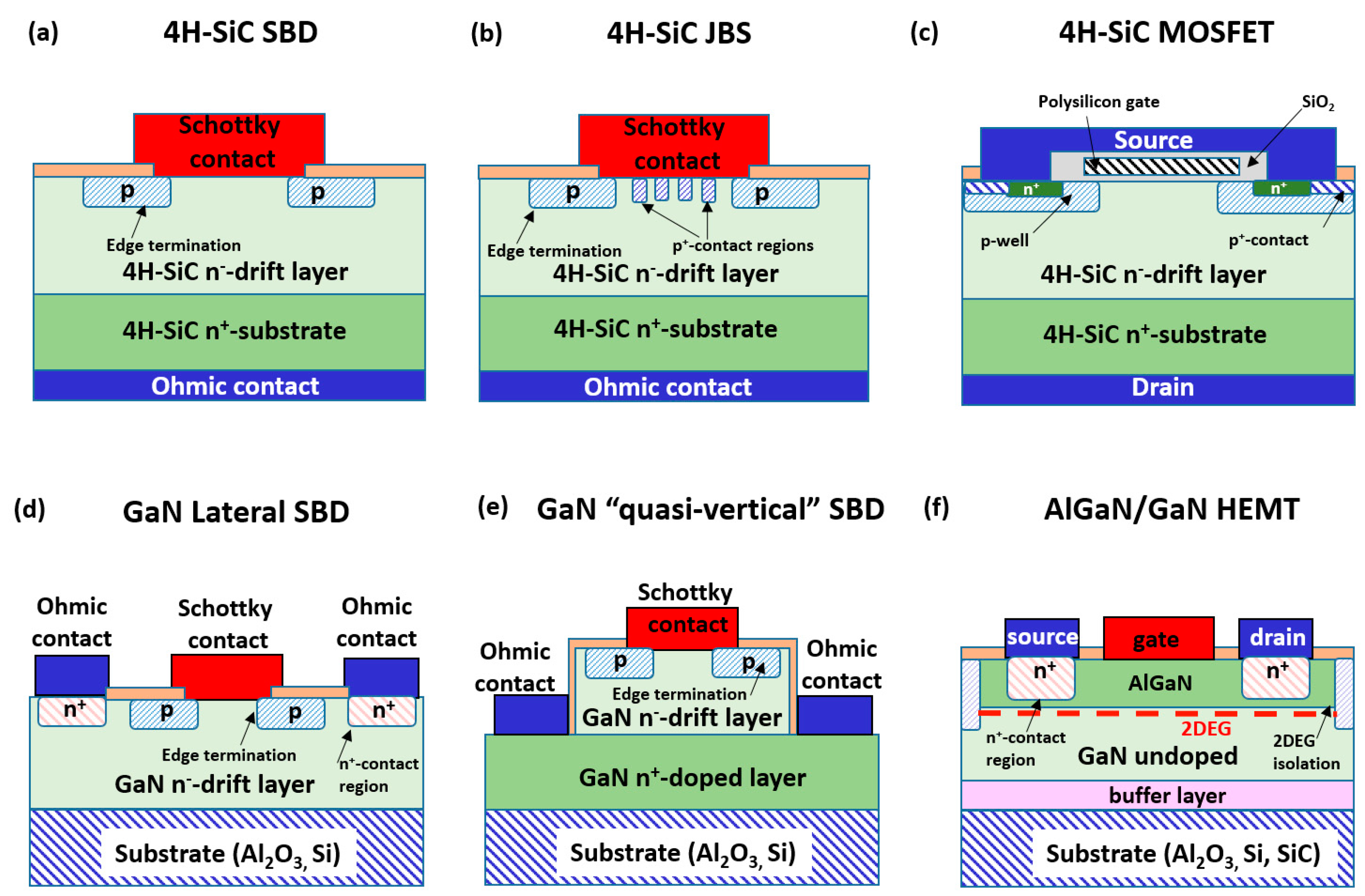
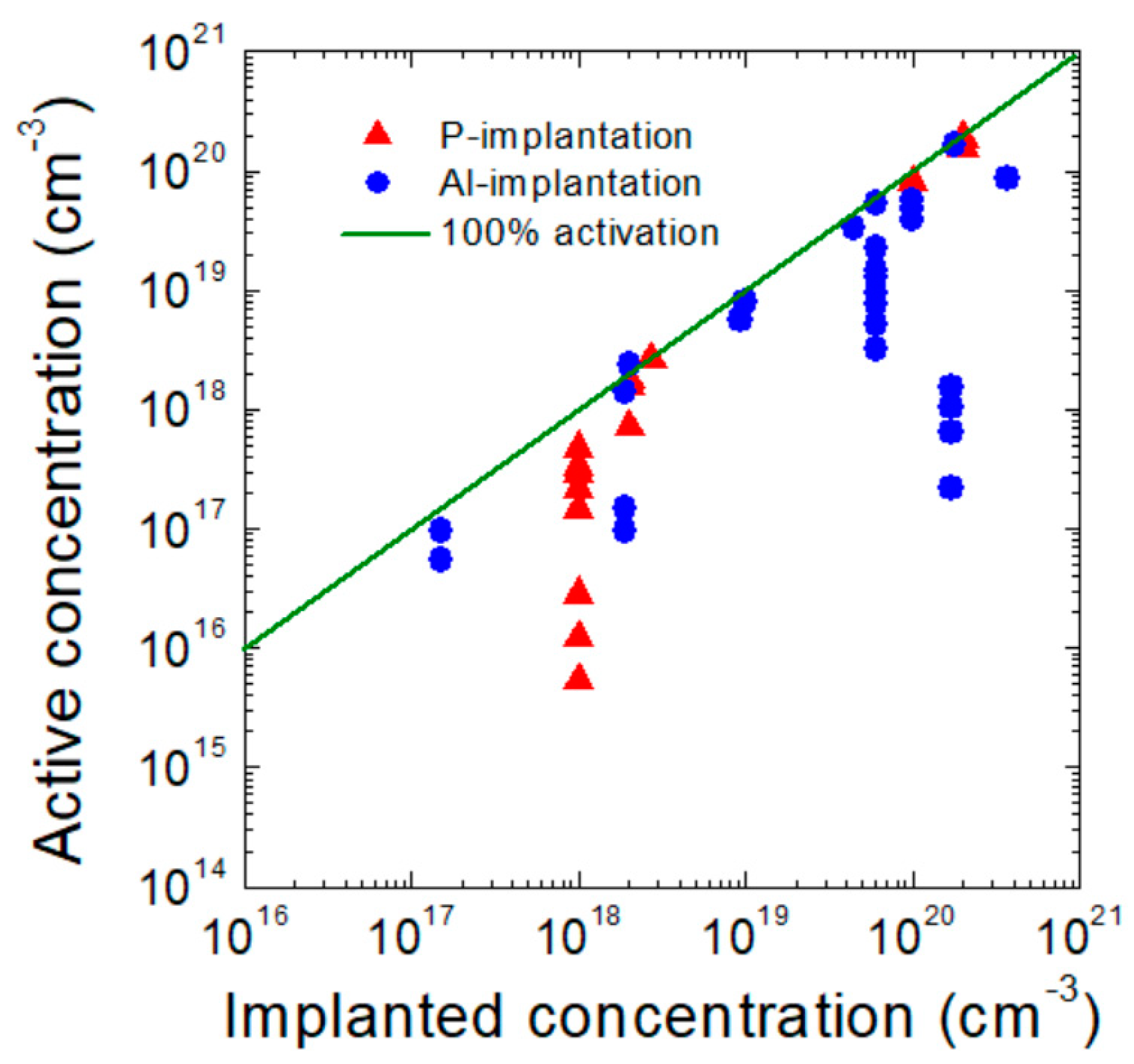
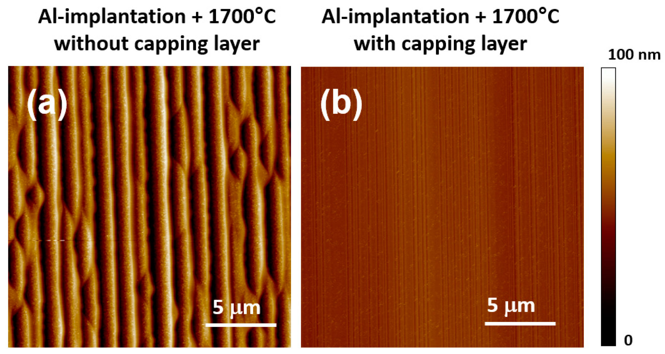
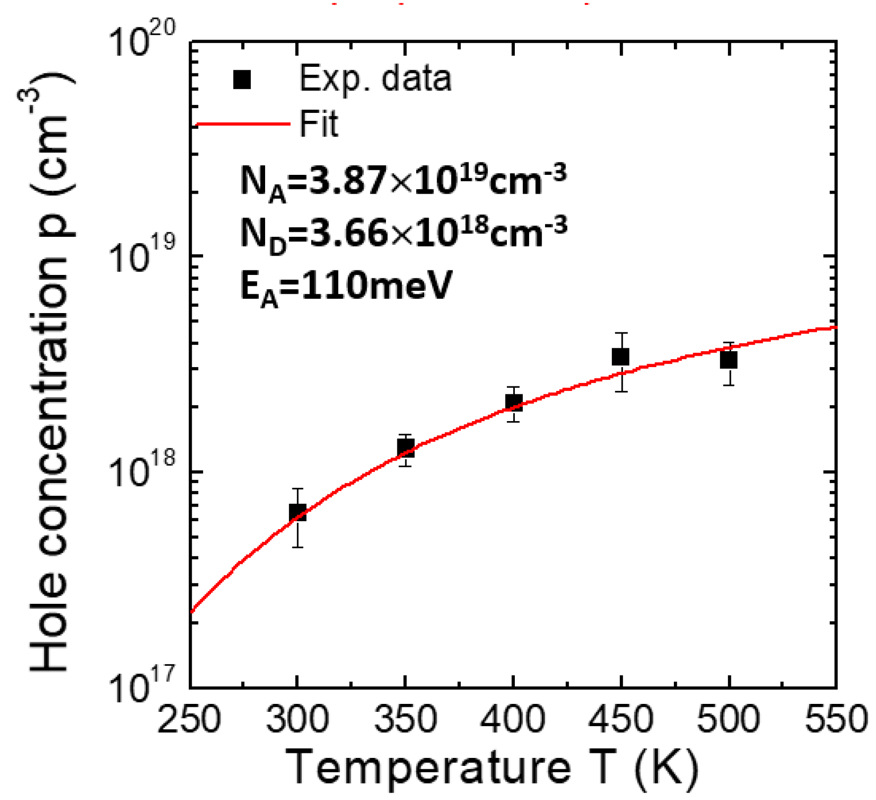
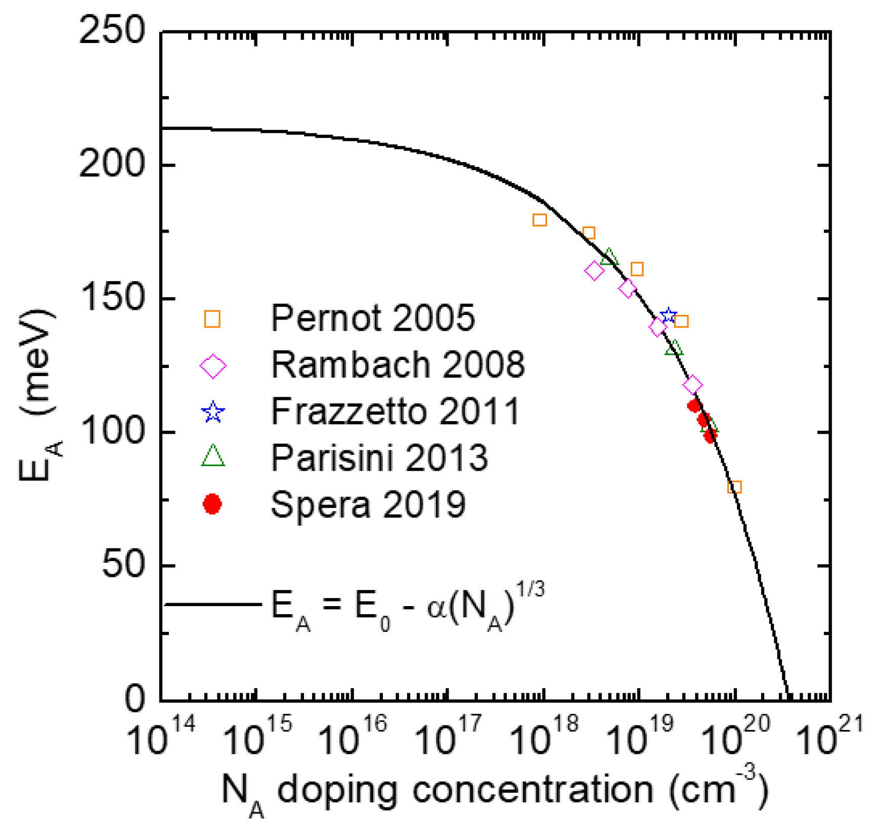
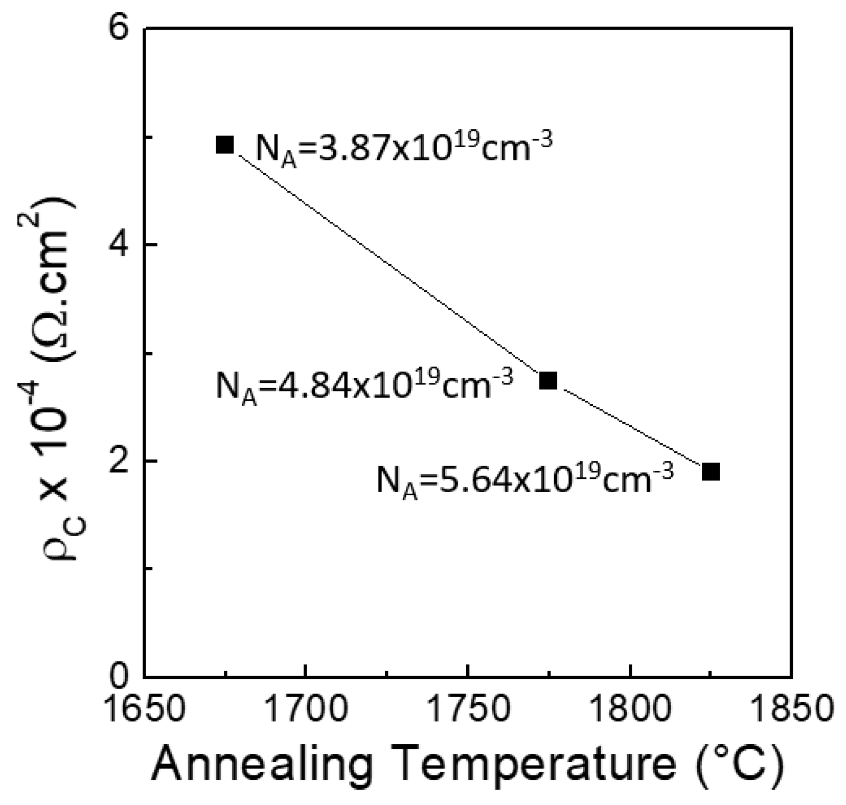
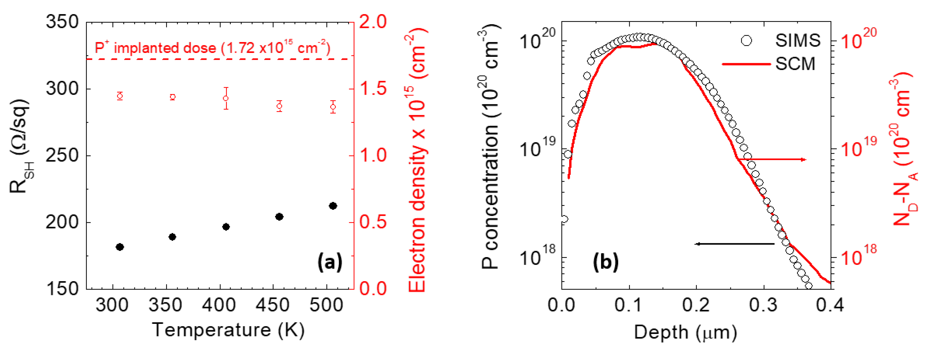
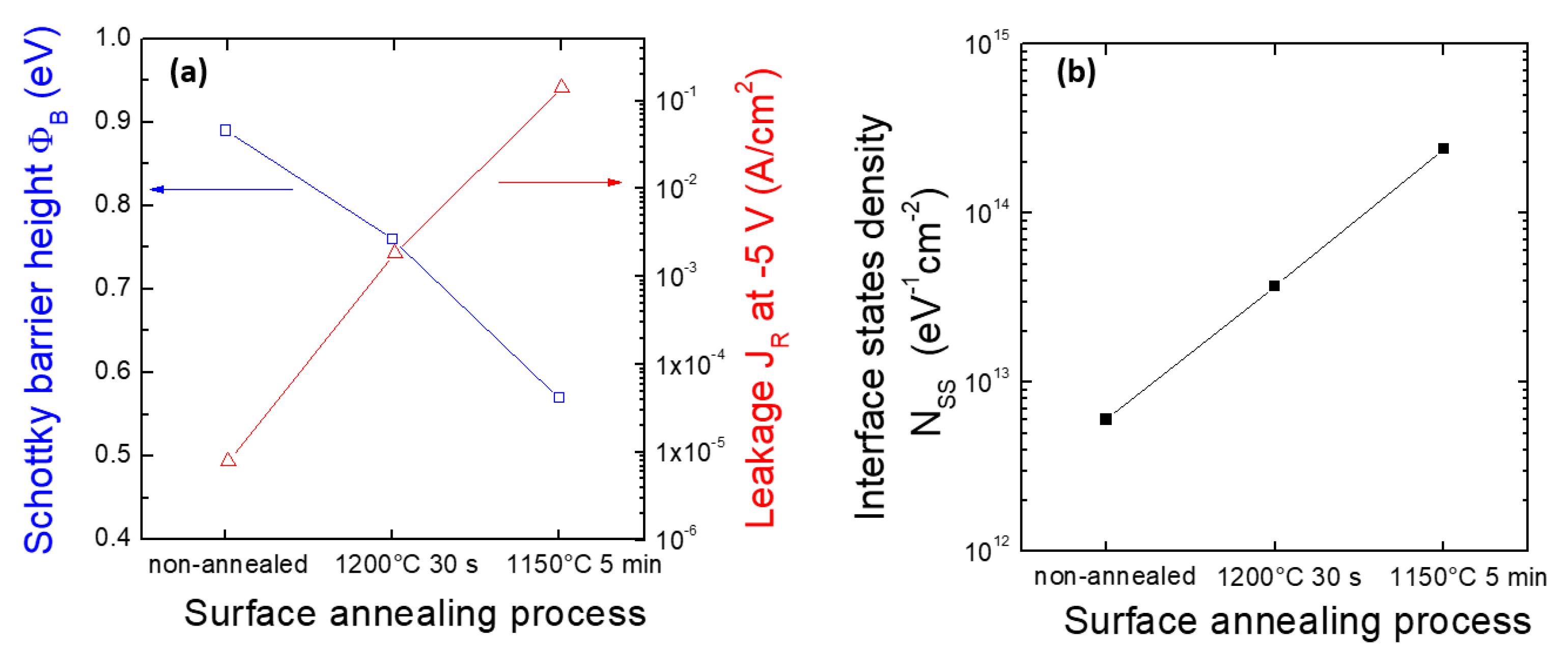
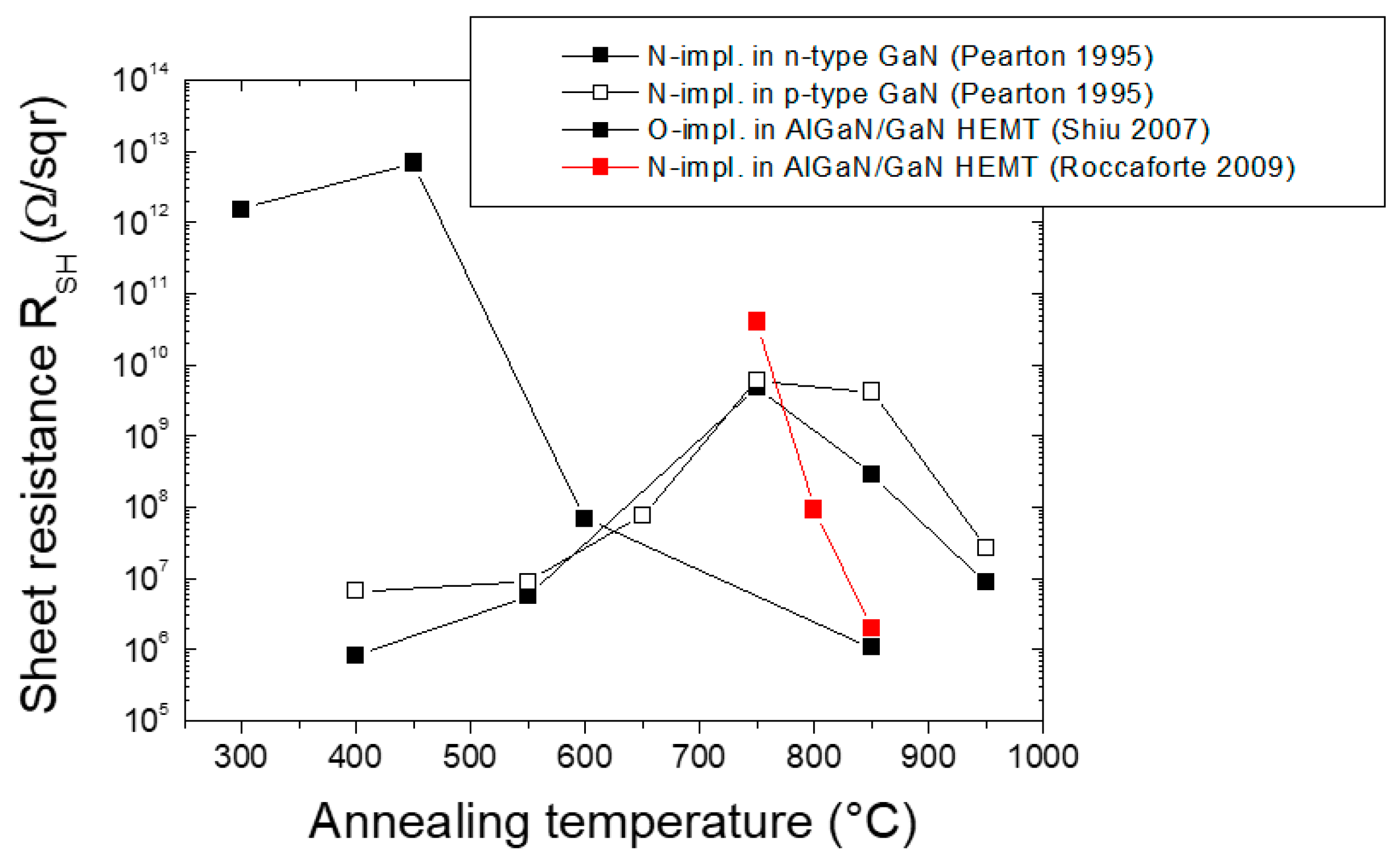
Table 1.
Ionization energies of the most common dopant species in 4H-SiC and GaN used for selective ion implantation doping in electronic devices [2,6,23,34,35,36,40]. The value of the ionization energies for N, P, and Al refer to the hexagonal (h) site of 4H-SiC [2].
| Material | N-Type Dopant | P-Type Dopant |
|---|---|---|
| SiC | N, P (~60 meV) | Al (~200 meV); B (280–300 meV) |
| GaN | Si (12–62 meV) | Mg (170–245 meV) |
Table 2.
Typical doping levels and implantation depths of the principal implanted regions that can be found in the SiC and GaN devices schematically shown in Figure 1.
Table 2.
Typical doping levels and implantation depths of the principal implanted regions that can be found in the SiC and GaN devices schematically shown in Figure 1.
| Implanted Region | Doping Level (cm−3) | Implantation Depth (μm) |
|---|---|---|
| Source/Drain, n+-contacts | 1019–1020 | 0.2–0.3 |
| MOSFET p-body | 1017–1018 | 0.4–0.8 |
| p+-contacts | 1019–1020 | 0.2–0.3 |
| Edge termination | 1016–1017 | 0.4–0.8 |
| 2DEG isolation | N.A. | 0.1–0.2 |
Table 3.
Electrical properties of the p-type-implanted 4H-SiC layers subjected to different post-implantation annealing at different temperatures (1675, 1775, and 1825 °C) [77].
Table 3.
Electrical properties of the p-type-implanted 4H-SiC layers subjected to different post-implantation annealing at different temperatures (1675, 1775, and 1825 °C) [77].
| Ann. Temp. (°C) | Resistivity (Ω cm) | EA (meV) | NA (cm−3) | ND (cm−3) | Al Activation | Compensation ND/NA |
|---|---|---|---|---|---|---|
| 1675 | 0.36 | 110 | 3.87 × 10¹⁹ | 3.66 × 10¹⁸ | 39% | 9.4% |
| 1775 | 0.29 | 105 | 4.84 × 10¹⁹ | 3.49 × 10¹⁸ | 48% | 7.2% |
| 1825 | 0.22 | 99 | 5.64 × 10¹⁹ | 3.48 × 10¹⁸ | 56% | 6.2% |
Table 4.
Survey of the literature data on the formation of Ohmic contacts on GaN and AlGaN/GaN heterostructures subjected to n-type selective doping by Si ion implantation and high-temperature post-implantation annealing for electrical activation of the dopant.
Table 4.
Survey of the literature data on the formation of Ohmic contacts on GaN and AlGaN/GaN heterostructures subjected to n-type selective doping by Si ion implantation and high-temperature post-implantation annealing for electrical activation of the dopant.
| Material | Implantation/Activation | Contact Formation | ρc (Ωcm2) | Ref. |
|---|---|---|---|---|
| p-GaN |
|
| 1.0 × 10⁻⁵ Ωcm2 | [145] |
| p-GaN |
|
| 1.5 × 10⁻⁶ Ωcm2 | [174] |
| p-GaN |
|
| 2.0 × 10⁻⁴ Ωcm2 | [175] |
| n-GaN |
|
| 1.0 × 10⁻⁵ Ωcm2 | [176] |
| n-GaN |
|
| 3.6 × 10⁻⁸ Ωcm2 | [177] |
| u.i.d. GaN |
|
| 2 × 10⁻⁷ Ωcm2 | [178] |
| n-GaN |
|
| 2.66 × 10⁻⁸ Ωcm2 | [179] |
| AGaN/GaN |
|
| 0.4 Ω mm | [146] |
| AGaN/GaN |
|
| 5.6 × 10⁻⁶ Ωcm2 | [180] |
| AGaN/GaN |
|
| 0.96 Ω mm | [181] |
| AGaN/GaN |
|
| 5.7 × 10⁻⁷ Ωcm2 | [182] |
Publisher’s Note: MDPI stays neutral with regard to jurisdictional claims in published maps and institutional affiliations. |
© 2022 by the authors. Licensee MDPI, Basel, Switzerland. This article is an open access article distributed under the terms and conditions of the Creative Commons Attribution (CC BY) license (https://creativecommons.org/licenses/by/4.0/).
Share and Cite
MDPI and ACS Style
Roccaforte, F.; Giannazzo, F.; Greco, G. Ion Implantation Doping in Silicon Carbide and Gallium Nitride Electronic Devices. Micro 2022, 2, 23-53. https://0-doi-org.brum.beds.ac.uk/10.3390/micro2010002
AMA Style
Roccaforte F, Giannazzo F, Greco G. Ion Implantation Doping in Silicon Carbide and Gallium Nitride Electronic Devices. Micro. 2022; 2(1):23-53. https://0-doi-org.brum.beds.ac.uk/10.3390/micro2010002
Chicago/Turabian StyleRoccaforte, Fabrizio, Filippo Giannazzo, and Giuseppe Greco. 2022. "Ion Implantation Doping in Silicon Carbide and Gallium Nitride Electronic Devices" Micro 2, no. 1: 23-53. https://0-doi-org.brum.beds.ac.uk/10.3390/micro2010002