Article

Micro-Optical Waveguides Realization by Low-Cost Technologies

by
Fabiana Cairone
1,
Francesco Gallo Afflitto
1,
Giovanna Stella
1,
Gianluca Cicala
2,
Mohamed Ashour
3,
Maïwenn Kersaudy-Kerhoas
3 and
Maide Bucolo
1,*
1
Department of Electrical, Electronic and Computer Science Engineering, University of Catania, Viale A. Doria 6, 95125 Catania, Italy
2
Department of Civil Engineering and Architecture, University of Catania, Viale A. Doria 6, 95125 Catania, Italy
3
School of Engineering & Physical Sciences, Heriot-Watt University, Edinburgh EH14 4AS, UK
*
Author to whom correspondence should be addressed.
Submission received: 29 November 2021 / Revised: 17 January 2022 / Accepted: 25 January 2022 / Published: 27 January 2022
(This article belongs to the Section Microscale Engineering)

Abstract

:
Microscale optofluidic devices are a category of microscale devices combining fluidic and optical features. These devices typically enable in-situ fluid flow measurement for pharmaceutical, environmental or biomedical applications. In micro-optofluidic devices, in order to deliver, as close as possible, the input light to the sample or a specific chip section and, collect the output signal, it is necessary to miniaturize optical components. In this paper, two low-cost technologies, 3D Printing PDMS-based and laser cutting PMMA-based (PDMS stands for Poly-dimethyl-siloxane and PMMA for Poly-methyl-methacrylate), were investigated as novel methods to realize micro-optical waveguides ( μ W G s ) comparing their performances. An ad-hoc master-slave protocol developed to realize PDMS components by 3D Printing has been fully optimized. The manufacturing technologies proposed require simple and low-cost equipment and no strictly controlled environment. Similar results are obtained for both the micro-optical waveguides realized. Their losses, disregarding the losses caused by the fibers’ alignment and the miss-match of the geometry with the waveguide, are of the order of 20 % , almost equivalent for both approaches (PDMS- μ W G and PMMA- μ W G ). The losses are of the order of 10 % when the PDMS- μ W G is shielded by a copper layer, with a significant improvement of the signal acquired. The results obtained show the possibility of using the two low-cost technologies presented for the realization of micro-optical waveguides suitable to be integrated in micro-optofluidic devices and the potential of creating micro-optical paths inside micro-embedded systems.

1. Introduction

Several approaches are available for detecting and monitoring fluids in microchannels, and in particular, among which, optical methods offer the advantage of obtaining non-invasive measurements [1,2]. In micro-optofluidic devices, in order to deliver, as close as possible, the input light to the sample or a specific chip section and, collect the output signal, it is necessary to miniaturize optical components [3]. Integration of optical components in a single device allows a rapid investigation of biological and chemical samples [4,5,6,7].
Different technologies can be exploited to realize micro-optical components. Conventionally, glass has been used as a material for the development of integrated optical circuits [8]. Glass allows low propagation losses, and easy matching to glass fibers. Microfabrication in glass involves traditional clean room procedures such as femtosecond laser writing, pulsed laser deposition (PLD), chemical vapor deposition (CVD), and selective wet etching. These fabrication methods are associated with high capital investment equipment and highly controlled clean room environment [8,9].
However, mature and more cost-effective prototyping methods may be applied to the fabrication of integrated optic components. Two aspects have a central role: the material itself and the fabrication method. These two aspects are strictly interlinked, indeed each manufacturing technology can be applied to a specific set of materials [10]. Among the most common manufacturing polymers, the Poly-dimethyl-siloxane (PDMS) [11] and Poly-methyl-methacrylate (PMMA) [12] are widely used in lab-on-a-chip applications [13,14,15] for their transparency, thermal stability, biocompatibility and low-cost.
PDMS is an excellent candidate for Lab on a Chip technologies and it is widely used in the fabrication of microfluidic devices as a replicating material [16]. PMMA is a material of choice for laser-based microengineering purposes due to its optical properties and mass-manufacturing compatibility [17,18,19,20].
In this paper, two approaches based on low-cost technologies, 3D Printing PDMS-based and laser cutting PMMA-based, were investigated as novel methods to realize micro-optical waveguides suitable for integration in micro-optofluidics devices [21,22], comparing their performances. An ad-hoc master-slave protocol developed to realize PDMS components by 3DPrinting has been fully optimized.
Soft-lithography [23] is a technology mainly used for the realization of PDMS micro-optical components such as: waveguides [24,25,26,27], micro-mirrors [28], and micro-lenses [29,30,31]. Example of applications for micro-flow monitoring in-vivo and in-vitro contexts are in [32,33]. Instead, to fabricate PMMA micro-optical components have been used reactive ion etching [34], hot embossing process [35], and direct ultraviolet (UV) writing [36]. In both cases, these fabrication methods require complex supporting equipment which are very expensive and to be used in highly controlled environment. Recently additive processes, collectively known as 3D Printing, have been identified as a progressive and effective technology and offer the possibility to quickly and inexpensively realize complex 3D structures at high resolution, displacing the need for soft-lithography. 3D printing offers rapid-prototyping capabilities in a large number of fields, including Lab-on-a-chip for biological and chemical applications [37]. The potential and the limitations of this technology in point-of-care devices realization were discussed in [38]. Since then a wide range of examples of micro-devices and realization protocols have been presented to exploit fully its potential [21,22,39,40,41].
Laser-based microengineering is another cost-effective and fast prototyping technique that can elegantly address the need for rapid design cycles [17], while still amenable to industrial scales. CO2 laser-based processes can be used to produce mold masters involved in the fabrication of microfluidic chips [42] and complex 3D and planar microstructures can be obtained with resolutions down to 100 nm [43]. Recently, PMMA has been used in the realization of optical components such as diffraction gratings for holographic storage [44], and optical waveguides [45].
The paper is organized as follows. In Section 2, the theoretical background of a micro-optical waveguide is presented, the design is described in detail, and the performance of PDMS and PMMA waveguides are compared by ray-tracing simulations. Then, the fabrication processes and the experimental results obtained during the characterization of the micro-optical waveguides in PDMS and in PMMA have been discussed. The results obtained show the possibility of using the two low-cost technologies presented for the realization of micro-optical waveguides suitable to be integrated in micro-optofluidic devices and the potential of creating micro-optical paths inside micro-embedded systems.

2. Materials and Methods

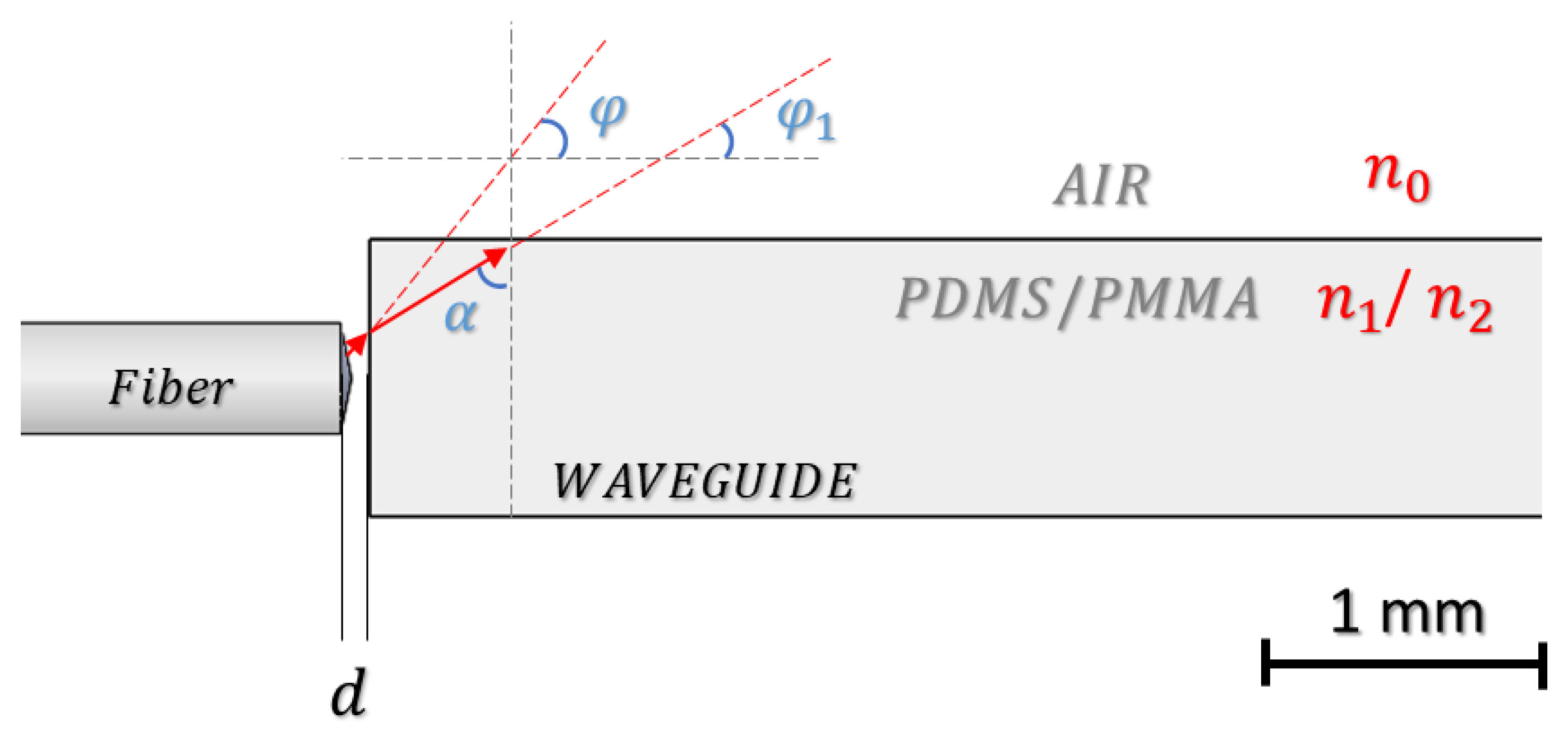
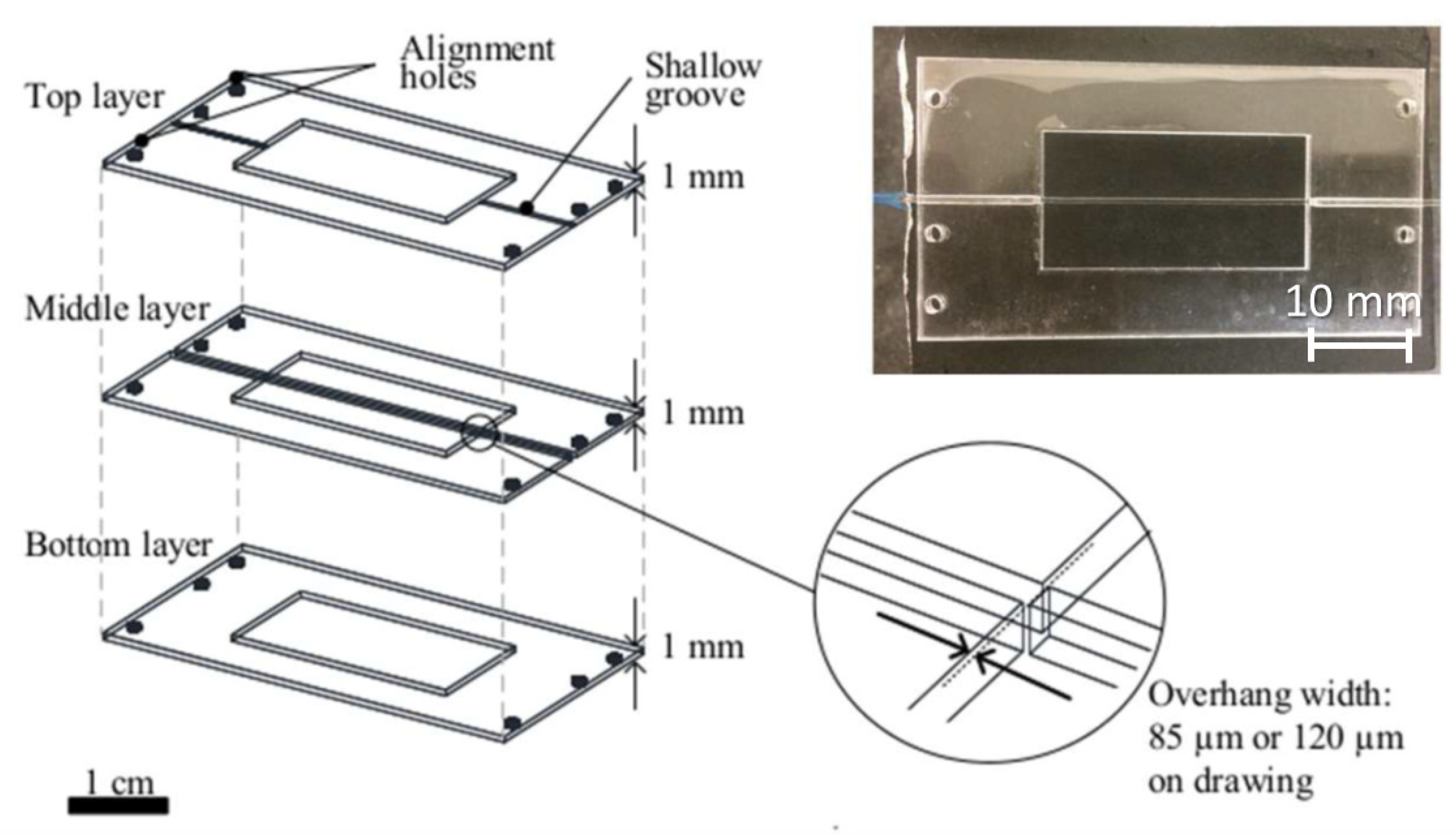
2.1. Design of the Micro-Optical Waveguide

A typical planar optical waveguide is formed by a strip of the guiding layer (core), with a higher refractive index, confined between the cladding layers, with a lower refractive index. In the proposed micro-waveguide (labeled μ W G ) the materials selected, the PDMS ( n 1 = 1.41 ) and the PMMA ( n 2 = 1.49 ), have been both surrounded by the air ( n 0 = 1 ). The light transmitted by a power source travels within the material whose refractive index is greater than that of the surrounding material to cause the total internal reflection phenomena.
The micro-waveguide was designed with a squared section of 1 mm side and a length of l = 4 cm (Figure 1). Two optical fibers were used: one to drive the laser beam toward the waveguide input section ( G 1 ), and the other to collect the beam at the waveguide output section ( G 2 ). The sections of the optical fibers faced with the μ W G were labeled { F 1 ; F 2 } . Assuming that the light is transmitted to the micro-waveguide by a laser system coupled with a fiber optic, other aspects to be taken into account in the design are the numerical aperture of the optical fiber ( N A , here set to 0.22 ), and the gap between the optical fiber and the waveguide (named d), that cause a change of direction in a certain number of emitted light rays.
From the Snell’s law to have the total internal reflection in the μ W G , the angle α between the rays and the perpendicular to the waveguide surface should have been greater than a critical value α m i n , as computed in Equations (1) and (2).
α m i n P D M S = arcsin ( n 0 n 1 · sin   90 ) = 45.2
α m i n P M M A = arcsin ( n 0 n 2 · sin   90 ) = 42.1
From the geometrical equality between angles (see in Figure 2) and based on the considered N A , it was possible to evaluate the angles { φ 1 P D M S , φ 1 P M M A } with which the rays enter respectively in the PDMS and PMMA micro-waveguide, and compute the actual value of the critical angels { α P D M S , α P M M A } confirming the condition of the total internal reflection (see the Equations (3)–(7)).
φ = arcsin ( N A )
φ 1 P D M S = arcsin ( n 0 n 1 · sin   φ ) = 8.97
φ 1 P M M A = arcsin ( n 0 n 2 · sin   φ ) = 8.49
α P D M S = 90 φ 1 P D M S = 81.03 > α m i n P D M S
α P M M A = 90 φ 1 P M M A = 81.51 > α m i n P M M A
The μ W G performance was evaluated by ray-tracing simulations (TracePro by Lamba Research Corporation) using the model in Figure 1, combined with the fiber optic model described in [21]. The laser source was assumed to emit 100 rays and positioned at a distance d ideally set to zero. The diameter of the input and output optical fiber { F 1 , F 2 } were set respectively to 365 μm and 1 mm.
In Figure 3 the radiance maps with the distribution and the percentage of light rays on the surfaces of the waveguide { G 1 , G 2 } and the output fiber F 2 are plotted. For all the maps, an area of 1 mm · 1 mm was considered. The rays distribution in Figure 3a,b are related to the input ( G 1 ) and the output ( G 2 ) sections of a PDMS- μ W G . The smaller diameter of the input fiber F 1 than that of the micro-waveguide G 1 allows for a good rays confinement inside the micro-waveguide. The same performance was obtained with the PMMA- μ W G . The rays distribution in Figure 3c,d are for the output fiber ( F 2 ) respectively in the case of PDMS and PMMA μ W G . The 15 % of rays dispersion obtained in the light transmission is due to the distance d between the waveguide and the fiber, the miss-match due to alignment and the abrupt change of the geometric interface.

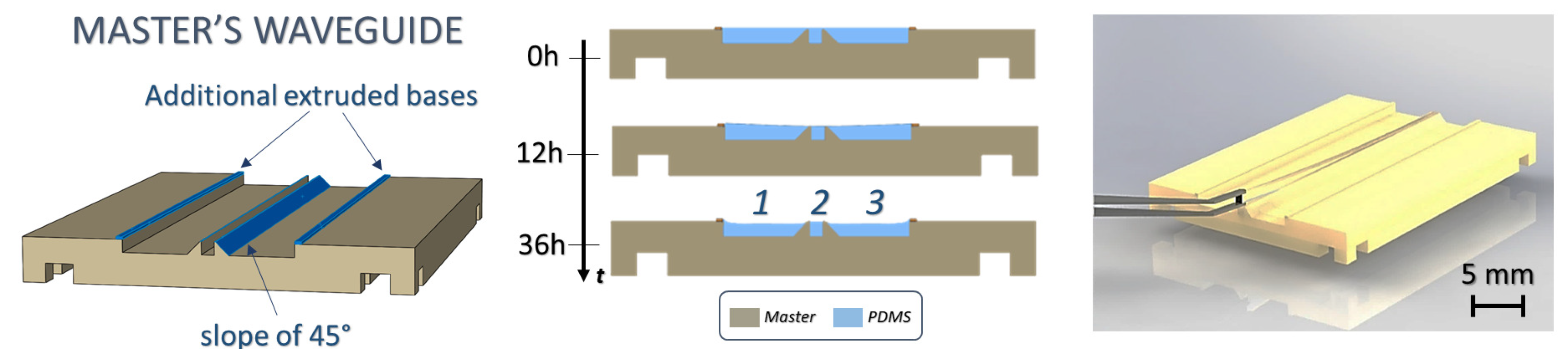
2.2. 3D Printing Fabrication Process PDMS-Based

A master-slave procedure is proposed to overcome 3D printing limitations with PDMS. The master-slave mold was printed by using an inkjet printer (Objet260 Connex1, Stratasys, Los Angeles, CA, USA). The material used for the mold was the VeroWhitePlus, while the FullCure705 was used as support. The support material is removable with a water jet and it is commonly used for printing hollow parts. The Object printer used in the present work is a professional inkjet, its use is quite consolidated and the accuracy range is well stated by the producers [46]. Due to the layer-by-layer construction, the resolution and surface quality is dependent on the orientation of the part. To reach a tread-off between the printing speed and the mold resolution, a flat orientation was set with 50 µm layer-by-layer thickness.
Generally, the master is obtained by overlaying thin layers of photo-sensible resin, and at each layer, the printer lights up the resin with UV rays in order to reticulate it. At the end, it could happen that, microscopically, the master is not perfectly reticulated and this could compromise the reticulation of the PDMS device in the master-slave procedure. In our previous work [21] a chemical treatment was proposed. In this work, an improvement of that protocol is presented by changing the chemical treatment with an UV treatment of 1 h at 35 ° C in an ad-hoc UV exposition chamber controlled in temperature. The neon tubes used for the UV treatment (Actinic BL TL 8W 10 UV-A G5, Philips, Amsterdam, Netherlands) have a wavelength of 300 nm and can deform the master in the case of uncontrolled exposure and consequently the PDMS device. A system for the temperature control inside the chamber was implemented by a micro-controller (with Arduino system) and a temperature sensor.
The silicone and the curing agent of PDMS (Sylgard 184 elastomer kit, Dow Corning, Midland, MI, USA) were mixed together according to the proportion (10:1). After the degassing, the PDMS was poured in the master and placed in an oven at 35   ° C for 36 h. Finally, the PDMS- μ W G was peeled from the mold. The master-slave protocol phases and the UV chamber are reported in the flow-diagram of Figure 4.
To enable an easy peeling of the PDMS- μ W G from the mold, it was necessary to include further optimization of the mold design. Two extruded bases were added, each with one wall inclined with a slope of 45 ° in proximity of the housing of the waveguide, as shown in Figure 5. This design allows for an auto-cutting process. The PDMS is uniformly distributed inside the site-1, site-2 and site-3, as shown in Figure 5. When the waveguide is removed, only the PDMS in site-2 will be peeled thanks to this process, leaving the remaining PDMS only in site-1 and site-3.
Additionally, a support structure for the PDMS- μ W G was realized, in a way that it will be surrounded by air. It was 3D-Printed having 4 pegs designed to touch as little as possible the PDMS to minimize the rays dispersion, see Figure 6a (on the left). In the micro-waveguide realized by Soft-Lithography in previous works [32,33], this problem is not dominant, because the smallest diameter few 100 μm minimizes the effects of rays dispersion. Additionally, for the alignment of the input and output fibers with the PDMS- μ W G , two PDMS frames have been used to surround the holder with two slots for the fibers insertions, the same approach used in [21]. In Figure 6 at the center it is shown the mounting scheme and on the right a photo of the complete micro-waveguide system.

2.3. Laser Cutting Fabrication Process PMMA-Based

The structure of the PMMA- μ W G was designed and laser cut in 2 mm and 1 mm thick sheets (Cast ClarexTM Acrylic, Easter Road Plastics, Edinburgh, UK) using a laser cutting instrument (Mini 18 30 W, Epilog Laser, Golden, CO, USA). The top and bottom layers were cut in 2 mm sheets at 70 % full power 21 W, 25 % full speed 21.25 mm/s, and 5000 Hz frequency, in two passes. The suspended μ W G was cut into a 0.2 mm layer with 2 bridge designs (d) at 85 μm, and 120   μ m. The 0.2 mm layer was cut at 25 % full speed 21.25 mm/s, and 45 % full power 13.5 W for the 85 μm design and 50 % full power 15 W for the 120 μm design. The laser pulse frequency was kept at 5000 Hz for all devices. The devices were then bonded using a two-minute thermal and solvent-assisted bonding reported in detail in [17]. In Figure 7, the steps in the realization of the PMMA- μ W G are shown on the left and a photo of the complete micro-waveguide system on the right.

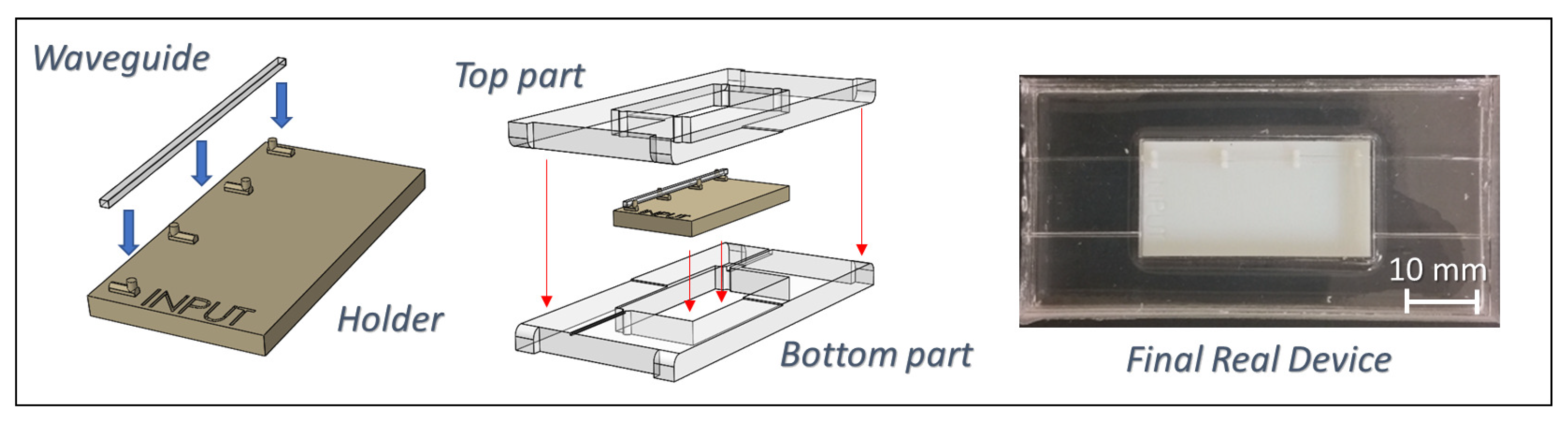
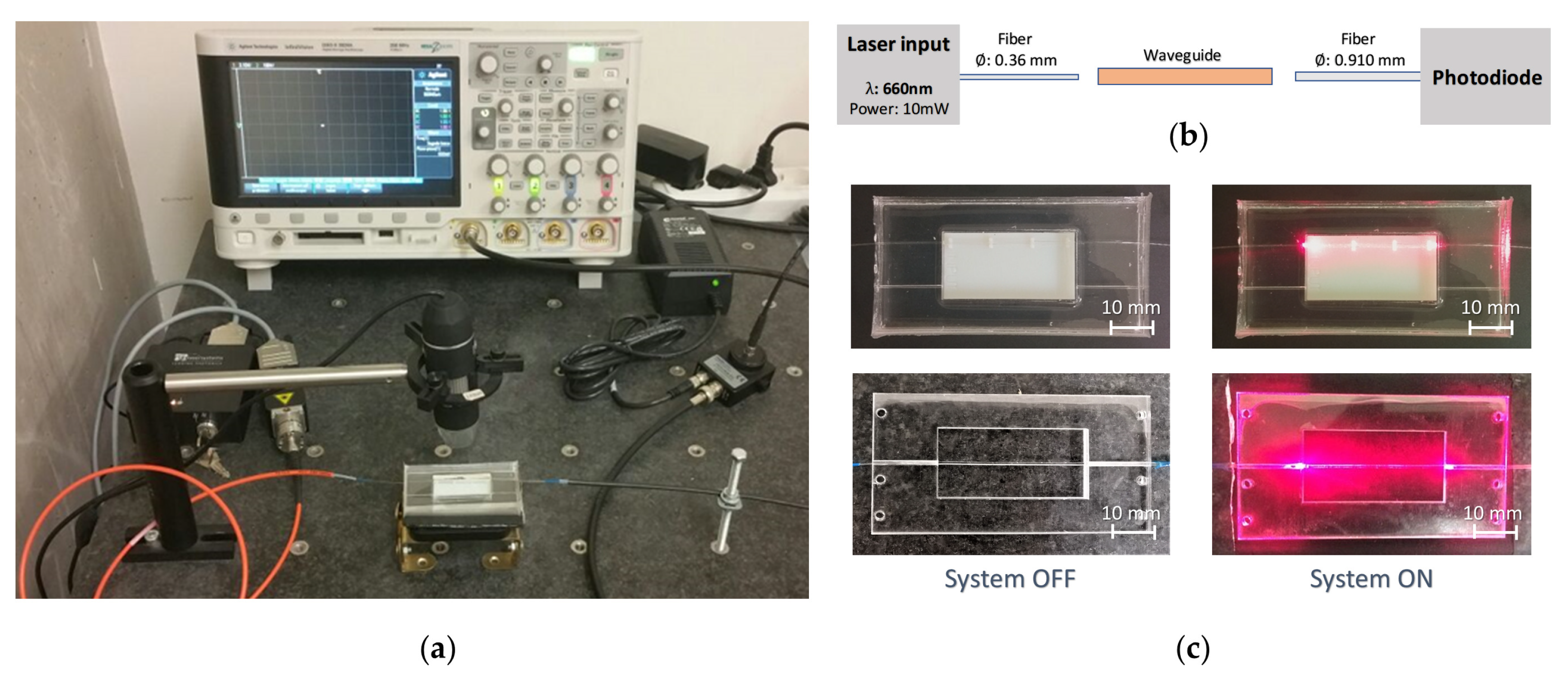
2.4. Experimental Set-Up

The experimental set-up for the micro-optical systems characterization is shown in Figure 8a. The input light source is a laser system (NovaPro 660-125, RGB Lasersystems, Kelheim, Germany), that generates a light beam with a wavelength of 660 nm and a maximum output power of 125 mW. The output acquisition system consists of a photo-diode (PDA100A, Thorlabs, Newton, NJ, USA) connected with a digital oscilloscope (SDS1102X, Siglent Technologies, Augsburg, Germany). The input and output systems are coupled by multi-mode optical fibers with core diameters { 910 ± 30 , 365 ± 14 } μm and N A = 0.22 .

3. Results and Discussion

Initially the roughness surface of the two μ W G s realized has been investigated. Their surfaces were analyzed by an Atomic Force Microscopy (AFM, NTEGRA, NT-MDT, Zelenograd, Russia). In Figure 9 the colormaps of the roughness distributions for both the μ W G s in a square surface of 5 μm side are shown. The color bar reports the surface height in the range [ 0 ; 100 ] nm for the PDMS- μ W G (Figure 9a) and [ 0 ; 70 ] nm for the PMMA- μ W G (Figure 9b). The root means square (RMS) and the roughness arithmetic average (RA) were chosen as rugosity parameters. The values measured for both the μ W G s show similar results, 6.410 nm/4.591 nm for the PDMS- μ W G and 6.564 nm/4.598 nm for the PMMA- μ W G . Additionally, the developed area surface ratio (Sdr) defined as the ratio between the real sample area and the nominal area were computed. It is 0.287 % for the PDMS- μ W G and 0.168 % for the PMMA- μ W G . Sdr, being extremely low, evidence the flattish of the surface for both the μ W G s . According to these results, it is possible to state that the surface roughness will not have a noticeable impact on the performance of the micro-optical components manufactured.
Before starting the micro-waveguide characterization, two experimental configurations { C 1 , C 2 } have been considered for the experimental set-up calibration and optimization, as shown in Figure 10 and Figure 11.
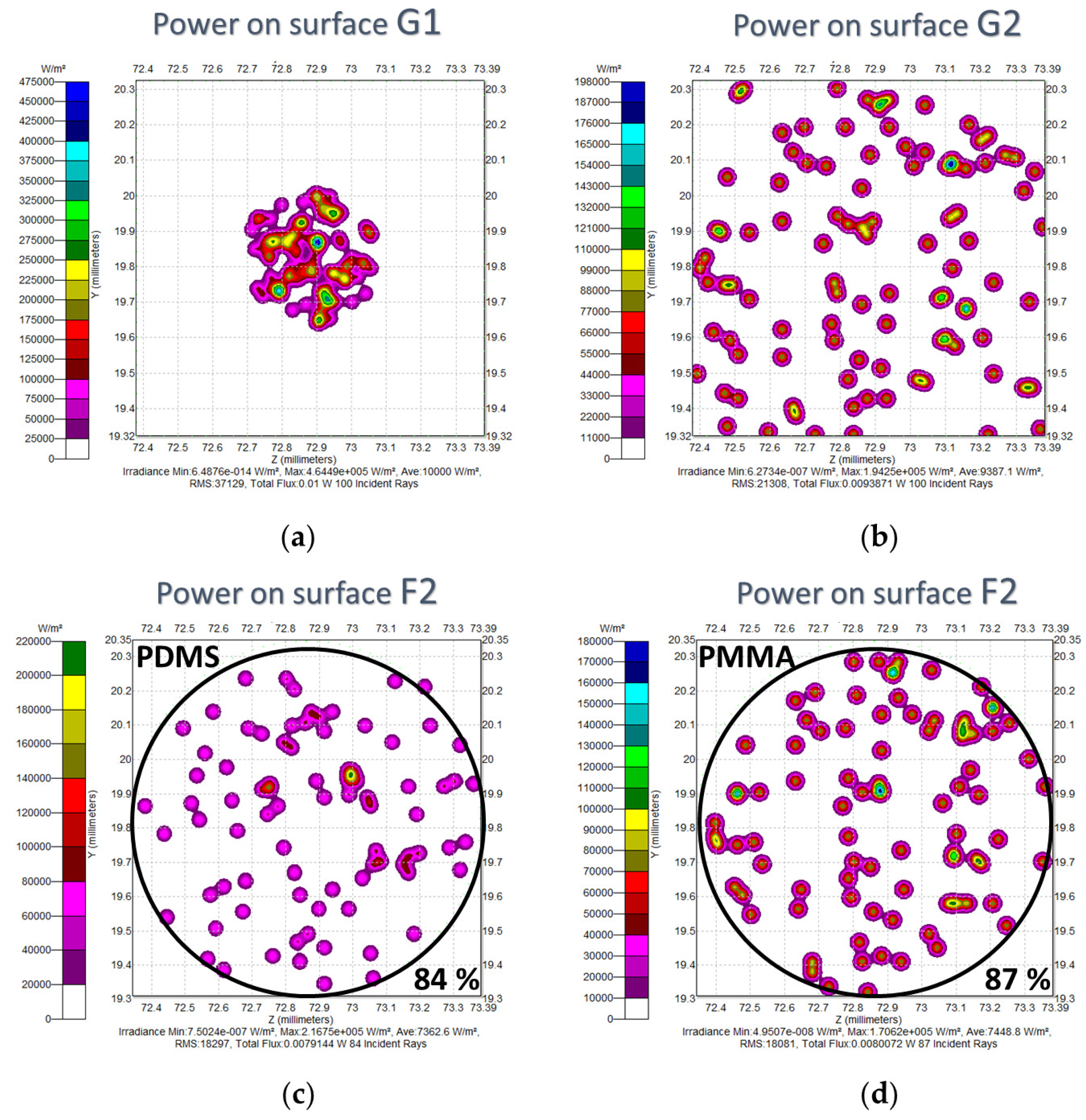
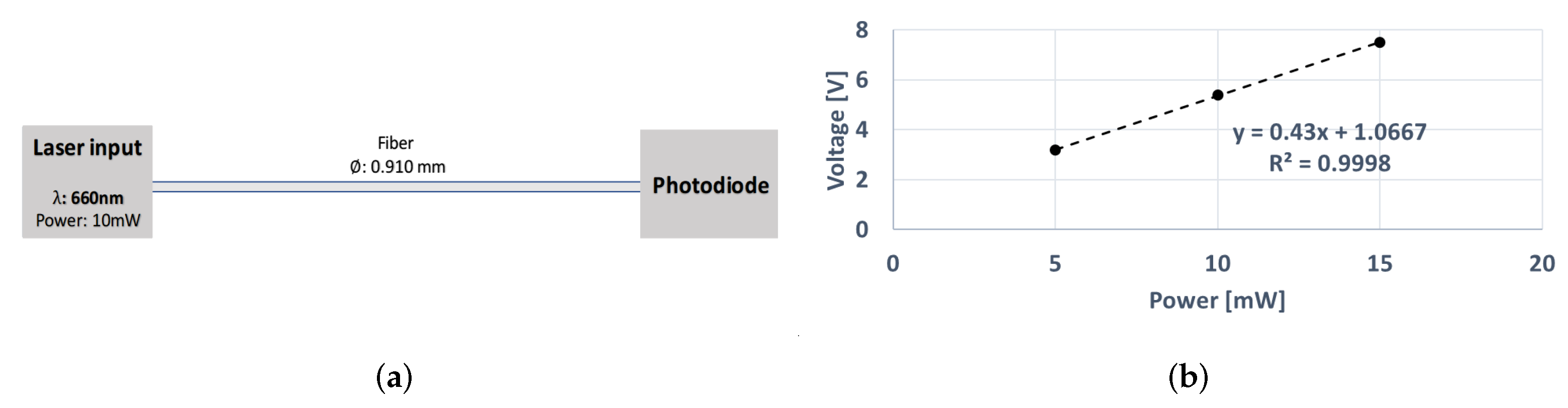
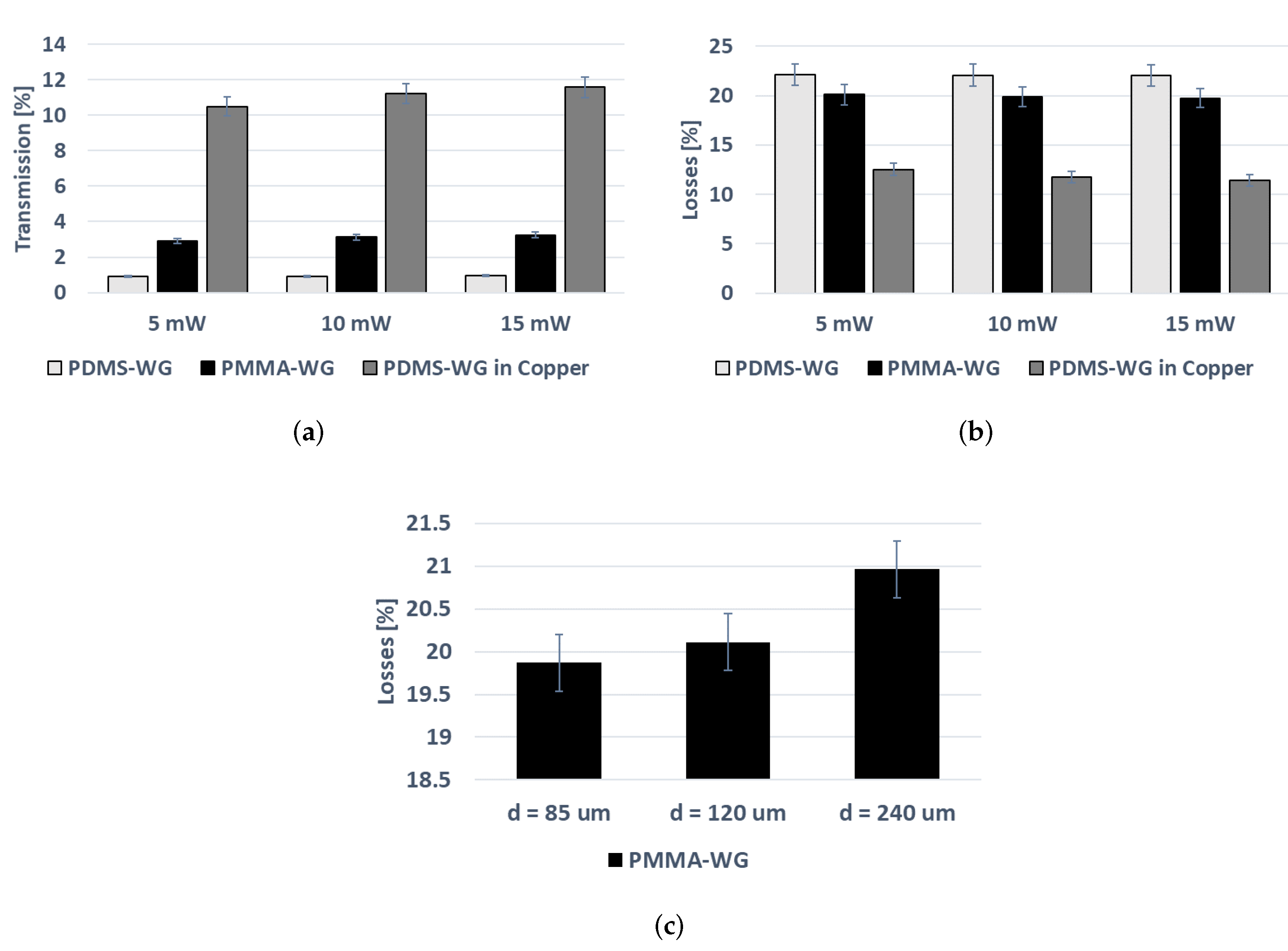
  • In condition C1, used for the set-up calibration, the laser light and the photo-diode were directly connected to the acquisition system by an optical fiber (core 910 μm, SMA to SMA, FG910LEC, Thorlabs, Newton, NJ, USA). The input laser power was increased in the set { 5 , 10 , 15 } mW and the values of voltages from the oscilloscope were read in order to obtain a calibration curve of the system, as shown in Figure 10b. The plot was mathematically interpolated and a linear increase is worth noticing. In this configuration no causes for light loss are present.
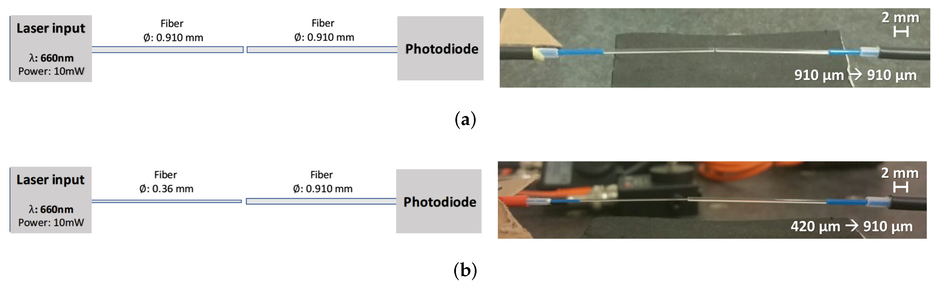
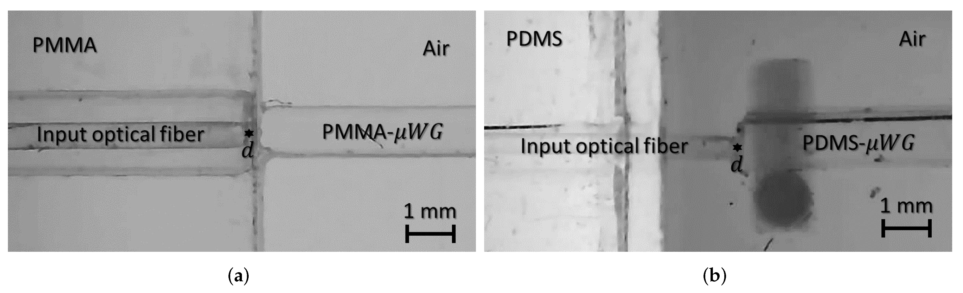
  • In the condition C2, used for the set-up optimization, the laser light was coupled initially with an optical fiber with a core of 910 μm and, subsequently with a core of 365 μm, both SMA to free-end (see Figure 11a,b). In both set-ups, those were aligned at a distance of about 100 μm with an optical fiber with a core of 910 μm (free-end to SMA) connected with the acquisition system. In Figure 11 the pictures of both set-ups are shown. Considering an input power laser of 10 mW, the voltage readings, considering the input fiber coupled with the laser with a core diameter of 910 μm and 365 μm, were respectively 3.0 V (losses of L 1 = 44 % ) and 3.6 V (losses of L 2 = 33 % ). The same percentage of losses are present also for the other input laser power, in accordance with the linearity shown in the curve calibration obtained in configuration ( C 1 ) (see Figure 10b). The loss was due to the light passage between media at the alignment section. A smaller fiber core diameter at the input than at the output assures minimal losses.
Then, the micro-waveguide was inserted in between the two fibers thanks to two alignment sections. The light, coming from the laser coupled with the input fiber ( 365 μm), passes through the first air gap to reach the waveguide then, at the output of the waveguide, after a second air gap is collected by the output fiber ( 910 μm) for the acquisition (see Figure 8b). The alignment between the fibers and the waveguides is indeed a crucial aspect, especially in the repeatability of measurement. Typically, the distance increases, then the optical signal acquired decreases. For this purpose, during the μ W G s characterization, the alignment between the fibers and the waveguide has been checked by a video camera in order to guarantee the repeatability of the measurement. As an example, in Figure 12 the images of both the PDMS and PMMA waveguides in the alignment phase at the input during the experiments are shown. In both cases, the distance between the input optical fiber, with a diameter of 365 μm, and the waveguide, with a diameter of 1 mm, was measured at around 85   μ m. The Figure 8c shows on the first row the PDMS- μ W G in the conditions of no-light passage and during the light-passage, and in the second row the PMMA- μ W G .
Being the μ W G side section of 1 mm, and assuming an expected loss of L 1 = 33 % at the first section and of L 2 = 44 % at the second, the envisaged overall losses reach the L = 77 % . Considering an input laser power of 10 mW, where the voltage reading was 5.4 V, the output voltage expected, taking into account only the 77 % of losses due to the fibers alignment and the miss-match of the geometry, will be about 1.2 V. In this case, no losses in the waveguide are considered.
In order to understand the optical performance of the μ W G , the transmission of the system was computed using the Equation (8), as the ratio between the output voltages reading and the input voltages reading, obtained during the calibration phase. It is possible to have the same, considering the values of the input power laser and the output power reading, given the correlation between power and voltage shown in Figure 10. The transmission parameter indirectly gives information about the losses that are present in the overall system. The losses are given by the sum of the losses due to the two fiber-waveguide alignments, as shown earlier, and the losses in the waveguide itself (see Equation (9)). The optical losses in the waveguide will be due to the interaction of the light with the materials, and also from the scattering of the rough waveguide boundaries.
T r a n s m i s s i o n = P o u t P i n = V o u t V i n = 1 L o s s e s
L o s s e s = L 1 + L 2 + L W G
In the bar charts of Figure 13, the transmissions and the losses values, in percentage, obtained for the PDMS and PMMA micro-waveguides are reported. During this characterization phase, the PDMS- μ W G and PMMA- μ W G were suspended in air. The distance between the fibers and PDMS- μ W G at the alignment was set to d = 85 μm. Based on the three designs realized for the PMMA micro-waveguides, the values of the distance at the alignment were set to {d1 = 85 μm, d2 = 120 μm, d3 = 240 μm}. The performance of the PMMA- μ W G and PDMS- μ W G , with a distance d equal to 85 μm between the input optical fiber and the waveguide, are comparable. In both cases, good sensitivity to laser power variation is observed (see Figure 13a,b). In Figure 8c, thanks to the PMMA- μ W G , with the laser light of 10 mW, it is worth noticing an increase of the losses by enlarging the alignment gap. The losses are around 20 % for the PMMA- μ W G with d 1 = 85 μm and around 22 % for the PDMS- μ W G with d 1 = 85 μm.
In these experiments, the performances obtained are independent of the laser temperature, thanks to the thermal stability properties of the materials investigated. This aspect is discussed in literature for the PDMS [47]. In particular, thermal decomposition starts at a temperature of about 200 ° C and reaches a peak at 310 ° C. Regarding the effect of temperature for PMMA the values of thermal decomposition start at 80 ° C, as shown in the experimental study [48]. Those results are a proof of concept on the possibility to miniaturize the optical components with both technologies and guide light into them maintaining optimal output illumination, even though the losses. It can be envisaged their reduction by the minimization of the gap at the alignment. Finally, Figure 13a,b shows also the results obtained by placing the PDMS- μ W G on a copper layer. In this case, the losses are around 10 % , with a significant improvement of the signal acquired. The μ W G s presented have similar performance with respect to those realized by standard technologies [24]. The attenuation of the optical signal detected in the 4 cm micro-waveguides are ∼20 dB for the PDMS- μ W G , ∼9 dB for the PDMS- μ W G in Copper and ∼15 dB for the PMMA- μ W G . These results compare favorably to similar data in the literature. In Cai et al. a micro-waveguide of 3 cm length realized by soft-lithography showed an attenuation of 23 dB [24]. The results obtained evidence the advantage of shielding the μ W G using a material with a lower refraction index. This modification combined with reduction of the air gap at the alignment can improve drastically micro-optical component performances.
On the basis of the results obtained and taking into account the possible field of application of the two proposed manufacturing processes, it can be stated that: PDMS- μ W G is particularly convenient to be integrated into lab-on-a-chip applications [24,49] generally used in the research context. Its fabrication by 3D printing technologies requires very simple equipment and no strictly controlled environment [50]. As far as PMMA- μ W G is concerned, it can be used in several areas of micro-engineering technology [31,51] due to the cost-effectiveness of the material and the possibility of massive manufacture in a short time using laser cutting technology [50].

4. Conclusions

In this paper, two low-cost manufacturing approaches, 3D Printing PDMS-based and laser cutting PMMA-based, were investigated as novel methods to realize micro-optical waveguides suitable to be integrated in micro-optofluidic devices for lab-on-a-chip application. An ad-hoc master-slave protocol developed from the authors to realize PDMS components by 3D Printing has been fully optimized. Comparing the performances of the micro-waveguides realized, similar results were obtained. Their losses, disregarding the losses caused by the fibers’ alignment and the miss-match of the geometry with the waveguide, are of the order of 20 % , almost equivalent for both approaches (PDMS- μ W G and PMMA- μ W G ). In order to increase the optical performance of the μ W G s , it is possible to cover them with a material with a lower refractive index, as shown in the results obtained for the PDMS- μ W G shielded by a copper layer. In this case, the losses are of the order of 10 % allowing a significant improvement of the acquired signal. It is important to underline that, with respect to the traditional methods, the 3D printing and the laser cutting techniques offer several advantages including the need of simple equipment, the use of low-cost materials and no strictly controlled environment.
The realization of μ W G s by the proposed low-cost manufacturing technologies represents a proof of concept to extend these approaches to other micro-optical components, suitable to be integrated in micro-optofluidic devices, and shows the potential of creating micro-optical paths inside micro-embedded devices.

Author Contributions

Conceptualization F.C., F.G.A., G.S., G.C., M.A., M.K.-K. and M.B.; methodology F.C., F.G.A., G.S., G.C., M.A., M.K.-K. and M.B.; validation F.C., F.G.A., G.S., G.C., M.A., M.K.-K. and M.B.; writing F.C., F.G.A., G.S., G.C., M.A., M.K.-K. and M.B. All authors have read and agreed to the published version of the manuscript.

Funding

The research activity was partially supported by University of Catania under the Grant Scheme PIACERI with the project MAF-moF “Materiali multifunzionali per dispositivi micro-optofluidici”.

Institutional Review Board Statement

Not applicable.

Informed Consent Statement

Not applicable.

Data Availability Statement

The CAD source files are available online at http://www.dees.unict.it/mbucolo/index.php/resources (accessed on 24 January 2022).

Acknowledgments

The authors thank M. E. Fragalà and the doctoral student M. Barcellona (both affiliated with the Department of Chemical Sciences at the University of Catania, Italy) for the analysis of the roughness surface performed with the AFM.

Conflicts of Interest

The authors declare no conflict of interest.

References

  1. Minzioni, P.; Osellame, R.; Sada, C.; Zhao, S.; Omenetto, F.G.; Gylfason, K.B.; Haraldsson, T.; Zhang, Y.; Ozcan, A.; Wax, A.; et al. Roadmap for optofluidics. J. Opt. 2017, 19, 093003. [Google Scholar] [CrossRef] [Green Version]
  2. Gagliano, S.; Stella, G.; Bucolo, M. Real-time detection of slug velocity in microchannels. Micromachines 2020, 11, 241. [Google Scholar] [CrossRef] [PubMed] [Green Version]
  3. Song, C.; Tan, S.H. A Perspective on the Rise of Optofluidics and the Future. Micromachines 2017, 8, 152. [Google Scholar] [CrossRef] [Green Version]
  4. Amiri, I.S.; Ariannejad, M.M.; Ali, J.; Yupapin, P. Design of optical splitter using ion-exchange method for DNA bio-sensor. J. King Saud Univ. Sci. 2019, 31, 549–555. [Google Scholar] [CrossRef]
  5. Guo, J.; Yang, C.; Dai, Q.; Kong, L. Soft and stretchable polymeric optical waveguide-based sensors for wearable and biomedical applications. Sensors 2019, 19, 3771. [Google Scholar] [CrossRef] [Green Version]
  6. Brammer, M.; Mappes, T. Modular platforms for optofluidic systems. Optofluidics 2013, 1, 1–10. [Google Scholar] [CrossRef]
  7. Ohkubo, T.; Terada, N.; Yoshida, Y. Minute particle detection using a light-wave-guide incorporated optical total analysis system. Microsyst. Technol. 2011, 17, 849–856. [Google Scholar] [CrossRef]
  8. Righini, G.C.; Chiappini, A. Glass optical waveguides: A review of fabrication techniques. Opt. Eng. 2014, 53, 071819. [Google Scholar] [CrossRef]
  9. Choudhury, D.; Ramsay, W.T.; Kiss, R.; Willoughby, N.A.; Paterson, L.; Kar, A.K. A 3D mammalian cell separator biochip. Lab Chip 2012, 12, 948–953. [Google Scholar] [CrossRef] [Green Version]
  10. Becker, H.; Locascio, L.E. Polymer microfluidic devices. Talanta 2002, 56, 267–287. [Google Scholar] [CrossRef]
  11. Wolf, M.P.; Salieb-Beugelaar, G.B.; Hunziker, P. PDMS with designer functionalities—Properties, modifications strategies, and applications. Prog. Polym. Sci. 2018, 83, 97–134. [Google Scholar] [CrossRef]
  12. Pawar, E. A review article on acrylic PMMA. IOSR J. Mech. Civ. Eng. 2016, 13, 1–4. [Google Scholar]
  13. Jiménez-Díaz, E.; Cano-Jorge, M.; Zamarrón-Hernández, D.; Cabriales, L.; Páez-Larios, F.; Cruz-Ramírez, A.; Vázquez-Victorio, G.; Fiordelisio, T.; Hautefeuille, M. Micro–Macro: Selective Integration of Microfeatures Inside Low-Cost Macromolds for PDMS Microfluidics Fabrication. Micromachines 2019, 10, 576. [Google Scholar] [CrossRef] [PubMed] [Green Version]
  14. Dietvorst, J.; Goyvaerts, J.; Ackermann, T.N.; Alvarez, E.; Muñoz-Berbel, X.; Llobera, A. Microfluidic-controlled optical router for lab on a chip. Lab Chip 2019, 19, 2081–2088. [Google Scholar] [CrossRef] [PubMed] [Green Version]
  15. Naskar, S.; Kumaran, V.; Basu, B. On the origin of shear stress induced myogenesis using PMMA based lab-on-chip. ACS Biomater. Sci. Eng. 2017, 3, 1154–1171. [Google Scholar] [CrossRef] [PubMed]
  16. McDonald, J.C.; Whitesides, G.M. Poly (dimethylsiloxane) as a material for fabricating microfluidic devices. Accounts Chem. Res. 2002, 35, 491–499. [Google Scholar] [CrossRef]
  17. Liga, A.; Morton, J.A.; Kersaudy-Kerhoas, M. Safe and cost-effective rapid-prototyping of multilayer PMMA microfluidic devices. Microfluid. Nanofluid. 2016, 20, 1–12. [Google Scholar] [CrossRef] [Green Version]
  18. Bridle, H.; Morton, J.; Cameron, P.; Desmulliez, M.P.Y.; Kersaudy-Kerhoas, M. Design of problem-based learning activities in the field of microfluidics for 12-to 13-year-old participants—Small Plumbing! Empowering the next generation of microfluidic engineers. Microfluid. Nanofluid. 2016, 20, 1–11. [Google Scholar] [CrossRef] [Green Version]
  19. Romoli, L.; Tantussi, G.; Dini, G. Experimental approach to the laser machining of PMMA substrates for the fabrication of microfluidic devices. Opt. Lasers Eng. 2011, 49, 419–427. [Google Scholar] [CrossRef]
  20. Klank, H.; Kutter, J.P.; Geschke, O. CO 2-laser micromachining and back-end processing for rapid production of PMMA-based microfluidic systems. Lab Chip 2002, 2, 242–246. [Google Scholar] [CrossRef]
  21. Cairone, F.; Gagliano, S.; Carbone, D.C.; Recca, G.; Bucolo, M. Micro-optofluidic switch realized by 3D printing technology. Microfluid. Nanofluid. 2016, 20, 61. [Google Scholar] [CrossRef]
  22. Cairone, F.; Davi, S.; Stella, G.; Guarino, F.; Recca, G.; Cicala, G.; Bucolo, M. 3D-Printed micro-optofluidic device for chemical fluids and cells detection. Biomed. Microdevices 2020, 22, 1–10. [Google Scholar] [CrossRef]
  23. Whitesides, G.M. The origins and the future of microfluidics. Nature 2006, 442, 368–373. [Google Scholar] [CrossRef]
  24. Cai, Z.; Qiu, W.; Shao, G.; Wang, W. A new fabrication method for all-PDMS waveguides. Sens. Actuators A Phys. 2013, 204, 44–47. [Google Scholar] [CrossRef]
  25. Pérez-Calixto, D.; Zamarrón-Hernández, D.; Cruz-Ramírez, A.; Hautefeuille, M.; Hérnandez-Cordero, J.; Velázquez, V.; Grether, M. Fabrication of large all-PDMS micropatterned waveguides for lab on chip integration using a rapid prototyping technique. Opt. Mater. Express 2017, 7, 1343–1350. [Google Scholar] [CrossRef]
  26. Chang-Yen, D.A.; Eich, R.K.; Gale, B.K. A monolithic PDMS waveguide system fabricated using soft-lithography techniques. J. Lightw. Technol. 2005, 23, 2088. [Google Scholar] [CrossRef] [Green Version]
  27. Wang, D.; Sheng, B.; Peng, L.; Huang, Y.; Ni, Z. Flexible and optical fiber sensors composited by graphene and PDMS for motion detection. Polymers 2019, 11, 1433. [Google Scholar] [CrossRef] [Green Version]
  28. Llobera, A.; Wilke, R.; Büttgenbach, S. Enhancement of the response of poly (dimethylsiloxane) hollow prisms through air mirrors for absorbance-based sensing. Talanta 2008, 75, 473–479. [Google Scholar] [CrossRef]
  29. Camou, S.; Fujita, H.; Fujii, T. PDMS 2D optical lens integrated with microfluidic channels: Principle and characterization. Lab Chip 2003, 3, 40–45. [Google Scholar] [CrossRef]
  30. Shao, G.; Qiu, W.; Wang, W. Fast replication of out-of-plane microlens with polydimethylsiloxane and curable polymer (NOA73). Microsyst. Technol. 2010, 16, 1471–1477. [Google Scholar] [CrossRef]
  31. Yang, L.; Wang, W. Design and fabrication of an on-chip micro flow cytometer with integrated micro-lens. Microsyst. Technol. 2019, 25, 2241–2247. [Google Scholar] [CrossRef]
  32. Sapuppo, F.; Llobera, A.; Schembri, F.; Intaglietta, M.; Cadarso, V.J.; Bucolo, M. A polymeric micro-optical interface for flow monitoring in biomicrofluidics. Biomicrofluidics 2010, 4, 024108. [Google Scholar] [CrossRef] [Green Version]
  33. Sapuppo, F.; Schembri, F.; Fortuna, L.; Llobera, A.; Bucolo, M. A polymeric micro-optical system for the spatial monitoring in two-phase microfluidics. Microfluid. Nanofluid. 2012, 12, 165–174. [Google Scholar] [CrossRef]
  34. Zhao, Y.; Wang, F.; Cui, Z.C.; Zheng, J.; Zhang, H.M.; Zhang, D.M.; Liu, S.Y.; Yi, M.B. Study of reactive ion etching process to fabricate the PMMA-based polymer waveguide. Microelectron. J. 2004, 35, 605–608. [Google Scholar] [CrossRef]
  35. Rezem, M.; Günther, A.; Rahlves, M.; Roth, B.; Reithmeier, E. Hot embossing of polymer optical waveguides for sensing applications. Procedia Technol. 2014, 15, 514–520. [Google Scholar] [CrossRef] [Green Version]
  36. Koo, J.S.; Smith, P.G.; Williams, R.B.; Riziotis, C.; Grossel, M.C. UV written waveguides using crosslinkable PMMA-based copolymers. Opt. Mater. 2003, 23, 583–592. [Google Scholar] [CrossRef]
  37. He, Y.; Wu, Y.; Fu, J.Z.; Gao, Q.; Qiu, J.J. Developments of 3D printing microfluidics and applications in chemistry and biology: A review. Electroanalysis 2016, 28, 1658–1678. [Google Scholar] [CrossRef]
  38. McDonald, J.C.; Chabinyc, M.L.; Metallo, S.J.; Anderson, J.R.; Stroock, A.D.; Whitesides, G.M. Prototyping of microfluidic devices in poly (dimethylsiloxane) using solid-object printing. Anal. Chem. 2002, 74, 1537–1545. [Google Scholar] [CrossRef]
  39. Chan, H.N.; Tan, M.J.A.; Wu, H. Point-of-care testing: Applications of 3D printing. Lab Chip 2017, 17, 2713–2739. [Google Scholar] [CrossRef]
  40. Hwang, Y.; Paydar, O.H.; Candler, R.N. 3D printed molds for non-planar PDMS microfluidic channels. Sens. Actuators A Phys. 2015, 226, 137–142. [Google Scholar] [CrossRef]
  41. Maia, J.M.; Amorim, V.A.; Alexandre, D.; Marques, P.V. Real-time optical monitoring of etching reaction of microfluidic channel fabricated by femtosecond laser direct writing. J. Lightw. Technol. 2017, 35, 291–2298. [Google Scholar] [CrossRef] [Green Version]
  42. Shiu, P.P.; Knopf, G.K.; Ostojic, M.; Nikumb, S. Non-lithographic fabrication of metallic micromold masters by laser machining and welding. Int. J. Adv. Manuf. Technol. 2012, 59, 157–167. [Google Scholar] [CrossRef] [Green Version]
  43. Ohrt, C.; Acar, Y.; Seidel, A.; Cheng, W.; Kiyan, R.; Chichkov, B.N. Fidelity of soft nano-imprint lithographic replication of polymer masters fabricated by two-photon polymerization. Int. J. Adv. Manuf. Technol. 2012, 63, 103–108. [Google Scholar] [CrossRef]
  44. Tolstik, E.; Kashin, O.; Matusevich, A.; Matusevich, V.; Kowarschik, R.; Matusevich, Y.I.; Krul, L.P. Non-local response in glass-like polymer storage materials based on poly (methylmethacrylate) with distributed phenanthrenequinone. Opt. Express 2008, 16, 11253–11258. [Google Scholar] [CrossRef]
  45. Hamid, H.H.; Rüter, C.E.; Thiel, D.V.; Fickenscher, T. Characteristics and crosstalk of optical waveguides fabricated in polymethyl methacrylate polymer circuit board. Appl. Opt. 2016, 55, 9017–9021. [Google Scholar] [CrossRef]
  46. Available online: https://www.stratasys-.com/3d-printers/objet-260-500-connex1 (accessed on 15 July 2021).
  47. Liu, M.; Sun, J.; Chen, Q. Influences of heating temperature on mechanical properties of polydimethylsiloxane. Sens. Actuators A Phys. 2009, 151, 42–45. [Google Scholar] [CrossRef]
  48. Abdel-Wahab, A.A.; Ataya, S.; Silberschmidt, V.V. Temperature-dependent mechanical behaviour of PMMA: Experimental analysis and modelling. Polym. Test. 2017, 58, 86–95. [Google Scholar] [CrossRef] [Green Version]
  49. Jandura, D.; Pudis, D.; Kuzma, A. Fabrication technology for PDMS ridge waveguide using DLW. Optik 2016, 127, 2848–2851. [Google Scholar] [CrossRef]
  50. Tsao, C.W. Polymer microfluidics: Simple, low-cost fabrication process bridging academic lab research to commercialized production. Micromachines 2016, 7, 225. [Google Scholar] [CrossRef] [Green Version]
  51. Asnawi, A.; Muntini, M.S.; Pramono, Y.H. Low-cost fabrication of optical waveguide as directional coupler using CO2 laser cutting. In Proceedings of the International Conference on Science and Technology, Yogyakarta, Indonesia, 7–8 August 2018; pp. 793–796. [Google Scholar]
Figure 1. (a) The geometry of the micro-waveguide. (b) A cartoon describing the pairing between the micro-waveguide and two optical fibers: one used to transmit the light and the other to collect it. The facing surfaces at the input and output section of the waveguide are labeled as { F 1 , G 1 } and { G 2 , F 2 } .
Micro 02 00008 g001
Figure 2. The geometrical model of the coupling between the fiber optic and micro-waveguide at the input section. The angle { φ 1 } with which the rays enter micro-waveguide, and the actual value of the critical angle { α } for the total internal reflection are correlated with the fiber optic N A ( φ = arcsin ( N A ) ) and the materials refractive index { n 0 , n 1 , n 2 } .
Micro 02 00008 g002
Figure 3. Radiance maps for the distribution and the percentage of light rays on the PDMS- μ W G surfaces (a) G 1 (b) G 2 , and on the surface of the output fiber F 2 after the beam passage through (c) the PDMS- μ W G and (d) PMMA- μ W G .
Micro 02 00008 g003
Figure 4. The phases of the master-slave protocol presented for the 3D Printing fabrication of PDMS devices. The CAD of the mold is printed and UV treated to guarantee the proper reticulation of the PDMS device.
Micro 02 00008 g004
Figure 5. (left) the design of the master for a safe extraction of the PDMS- μ W G ; (center) the auto-cutting PDMS process during the PDMS curing; (right) the waveguide extraction.
Micro 02 00008 g005
Figure 6. Steps in the realization of the PDMS- μ W G . On the left the holder designed to support the micro-optical component; at the center mounting scheme of the holder and the top and bottom PDMS layer used for the fibers alignment; on the right the photo of the complete micro-optical system.
Micro 02 00008 g006
Figure 7. Steps in the realization of the PMMA- μ W G . On the left the CAD of the three cut layers with a zoom in the alignment area and on the right the photo of the final device.
Micro 02 00008 g007
Figure 8. The experimental set-up and the laboratory equipment. (a) At the input the laser source connected to a multi-mode optical fiber. At the output, a fiber coupled with a photo-diode and a digital oscilloscope used for the reading. Both fibers are aligned with the μ W G . (b) A cartoon of the set-up used for the μ W G characterization, where it is placed in between the optical fibers. (c) The pictures of both μ W G s in the conditions of no-light passage and during the light-passage. On the first row the PDMS- μ W G and in the second row the PMMA- μ W G .
Micro 02 00008 g008
Figure 9. The colormaps of the roughness distributions in 2D and 3D for both the μ W G s in a square surface of 5 μm side. The color bar reports the surface height in the range [ 0 ; 100 ] nm for the PDMS- μ W G (a) and [ 0 ; 70 ] nm for the PMMA- μ W G (b).
Micro 02 00008 g009
Figure 10. (a) A cartoon of the configuration ( C 1 ) for the calibration of the experimental set-up. The laser light and the photo-diode are directly connected. (b) Calibration curve of the configuration ( C 1 ) where the values of Voltage { 3.2 , 5.4 , 7.5 } V obtained from the photo-diode are plotted versus the input laser power { 5 , 10 , 15 } mW.
Micro 02 00008 g010
Figure 11. The cartoons and the pictures of the configuration ( C 2 ) for the optimization of the experimental set-up. The laser light and the photo-diode are connected by two aligned optical fibers. The laser light is coupled respectively with an optical fiber with a core of 910 μm (a) and 365 μm (b) and aligned at a distance of about 100 μm with an optical fiber with a core of 910 μm for the light acquisition.
Micro 02 00008 g011
Figure 12. The images of the PDMS- μ W G (a) and PMMA- μ W G (b) in the alignment phase at the input during the experiments. The distance d between the input optical fiber, with a diameter of 365 μm, and the waveguide, with a diameter of 1 mm, was measured at around ∼ 85 μm.
Micro 02 00008 g012
Figure 13. (a,b) Bar Charts of the transmissions and losses obtained for a PDMS- μ W G ( d = 1 mm) and a PMMA- μ W G ( d 1 = 85 μm) suspended in air, and a PDMS- μ W G placed on a copper layer ( d = 1 mm). The input laser power spans the values of { 5 , 10 , 15 } mW. (c) The values of the distance at the alignment for the PMMA- μ W G were set {d1 = 85 μm, d2 = 120 m, d3 = 240 μm} and the laser power is 10 mW.
Micro 02 00008 g013
Publisher’s Note: MDPI stays neutral with regard to jurisdictional claims in published maps and institutional affiliations.

