
The Development of iDPC-STEM and Its Application in Electron Beam Sensitive Materials


Beijing Key Laboratory of Microstructure and Properties of Solids, Faculty of Materials and Manufacturing, Beijing University of Technique, Beijing 100124, China
*
Authors to whom correspondence should be addressed.
Molecules 2022, 27(12), 3829; https://0-doi-org.brum.beds.ac.uk/10.3390/molecules27123829
Submission received: 1 May 2022
/
Revised: 31 May 2022
/
Accepted: 1 June 2022
/
Published: 14 June 2022
(This article belongs to the Special Issue Advanced Energy Storage Materials and Their Applications)
Abstract
:The main aspects of material research: material synthesis, material structure, and material properties, are interrelated. Acquiring atomic structure information of electron beam sensitive materials by electron microscope, such as porous zeolites, organic-inorganic hybrid perovskites, metal-organic frameworks, is an important and challenging task. The difficulties in characterization of the structures will inevitably limit the optimization of their synthesis methods and further improve their performance. The emergence of integrated differential phase contrast scanning transmission electron microscopy (iDPC-STEM), a STEM characterization technique capable of obtaining images with high signal-to-noise ratio under lower doses, has made great breakthroughs in the atomic structure characterization of these materials. This article reviews the developments and applications of iDPC-STEM in electron beam sensitive materials, and provides an outlook on its capabilities and development.
1. Introduction
With the development of material science, the corresponding relationship between material structures and their properties has become more precise and refined. Compared with an overall periodic crystal structure [1,2,3,4], some local structures, such as interfaces, defects, and surfaces [5,6,7], can better reflect this relationship. Since these structures are often non-periodic, real-space characterization is often required, which has been greatly facilitated by the development of electron microscopy (EM). By using spherical aberration and chromatic aberration correctors [8,9], huge improvements in image resolution have been achieved. The adoption of direct detection electron counting (DDEC) has greatly improved the detective quantum efficiency (DQE) [10,11], resulting in further improvements in imaging quality, as shown in Figure 1.
However, the electron beam with higher energy can cause some damage to the material structure while carrying the structural information of the sample [12,13]. Especially for electron-beam sensitive materials such as MOFs [14,15,16], two-dimensional materials [12], and lithium-ion batteries [17], it is extremely serious and difficult to ignore. Therefore, the use of electron microscopy to characterize the structure of such materials is both important and challenging.
Damage caused by the electron beam is inevitable, and its formation mechanism is complex. Figure 2 shows the main mechanisms of electron beam damage in STEM, including knock-on damage, radiolysis damage, electrostatic charging, and heating. During the actual characterization process, multiple mechanisms often coexist, influence, and even transform each other under certain conditions. A series of characterization methods for different types of electron beam-sensitive materials have been carried out [18,19,20,21,22,23], iDPC-STEM [24,25,26] is one of the most versatile and promising tools at present.
Figure 3 shows the number of applications of iDPC-STEM in the characterization of electron beam sensitive materials (low-dose EM techniques). It can be seen that its proportion is currently at a low level, which is greatly related to the fact that the technology is in the early stage of development and lacks the process of combining with actual characterization work. As the intersection of materials science and electron microscopy, differences in the field are also one of the reasons for its obvious advantages but limited applications.
The deepening understanding of material structure is bound to promote rapid advancement in materials and related fields. This paper will introduce the development history, imaging principle and application status of iDPC-STEM in real-space EM characterization, and summarize and prospect the application prospect of this method in atomic-scale imaging, hoping to promote the development of electron beam-sensitive materials structural characterization.
2. Technological Development
Phase contrast was proposed by Rose [27] in 1974. In the same year, Dekkers and De Lang [28] pointed out that the technique of obtaining images by using the relative signal difference of partition detectors could be applied to scanning transmission electron microscopy [29], which introduced the differential phase contrast (DPC) technique into electron microscopy. Waddell et al. [30] pointed out the basis for its application in electron microscopy, which could be achieved through a “first moment” detector to measure the momentum transferred to the probe and obtain the centroid of the intensity of electron beam illumination. In 1977, Rose [31] again reviewed DPC techniques using partitions in STEM and proposed execution time integrals to restore the phase. At that time, the understanding of the influence of noise and the linear relationship between the momentum transfer (centroid position) of the electron beam and the phase transfer function (phase contrast) of the sample, its physical significance, and an in-depth mathematical proof had not yet been determined. In 1978, Chapman et al. [32] began using the DPC technique for the quantitative study of magnetic structures in ferromagnetic thin films. For the next three decades, it was mainly used to study magnetic samples [33,34,35,36,37]. During this period, the theoretical research of DPC imaging was mainly based on optical microscopy, while imaging research based on electron microscopy was rarely mentioned [38].
In 2010, Shibata [39] and others once again introduced the DPC technique into electron microscopy and obtained the first convincing single-segment imaging experimental results of non-magnetic samples with atomic resolution. Since then, the DPC technique has been applied to electron microscopy. During its continuous development [40,41,42,43,44], the algorithms have been continuously optimized. The collection of local electric potential (DPC-STEM), local charge density (dDPC-STEM), and local electrostatic potential (iDPC-STEM) are all based on the COM approximate technique, and the three complement each other. In 2016, mathematical proof of the linear relationship between the COM position and the phase contrast of the sample was achieved, and the iDPC technique experimental image was provided for the first time.
3. Technological Principle
For non-magnetic samples, basic electrostatics stipulates that the electric field (conservative vector field) of the sample is the gradient (differential) of the electrostatic potential field (scalar field) of the sample. Electrons passing through the sample are affected by this electric field. If the sample is very thin, the electric field at the point of impact will deflect electrons in proportion to their in-plane components. This deflection can be measured by detecting the position of electrons on the far-field detector to obtain the corresponding convergent beam electron diffraction (CBED) pattern, thereby obtaining information about the position of the center of mass. The differential phase contrast (DPC) technique is used to measure the deflection of the electron (beam), i.e., the position of the center of mass [45]. When multiple zoned detectors are used, the smallest changes will be captured, and the centroid position of the direction can be calculated based on the alignment difference. This is the case with iDPC, which is the same as dDPC and DPC, which use partitioned probes to collect local signals to achieve COM position approximation.
Figure 4 shows a schematic of an iDPC-STEM. Through A-C and B-D, the COMx and COMy are obtained, then a high-quality image is obtained by a fitting calculation. This is a direct phase imaging process and is dependent on atomic number. The larger the atomic number, the stronger the scattering, and the brighter the signal. This imaging principle causes the intensity in iDPC images to be linearly related to atomic number, whereas in high-angle annular dark field (HAADF) images, the intensity is approximately proportional to the square of the atomic number; therefore, more information related to lighter elements can be obtained by using iDPC-STEM.
In addition, due to the higher electron utilization rate and the integration processes [46,47] (which remove a large part of the noise), it can achieve a high signal-to-noise (SNR) ratio under a lower dose. These levels are difficult to achieve using traditional characterization methods [48,49]: typically, the minimum electron beam dose required to obtain an image with enough SNR is 103 e−/Å2, but iDPC-STEM can achieve around 10 e−/Å2.
4. iDPC-STEM Advantages
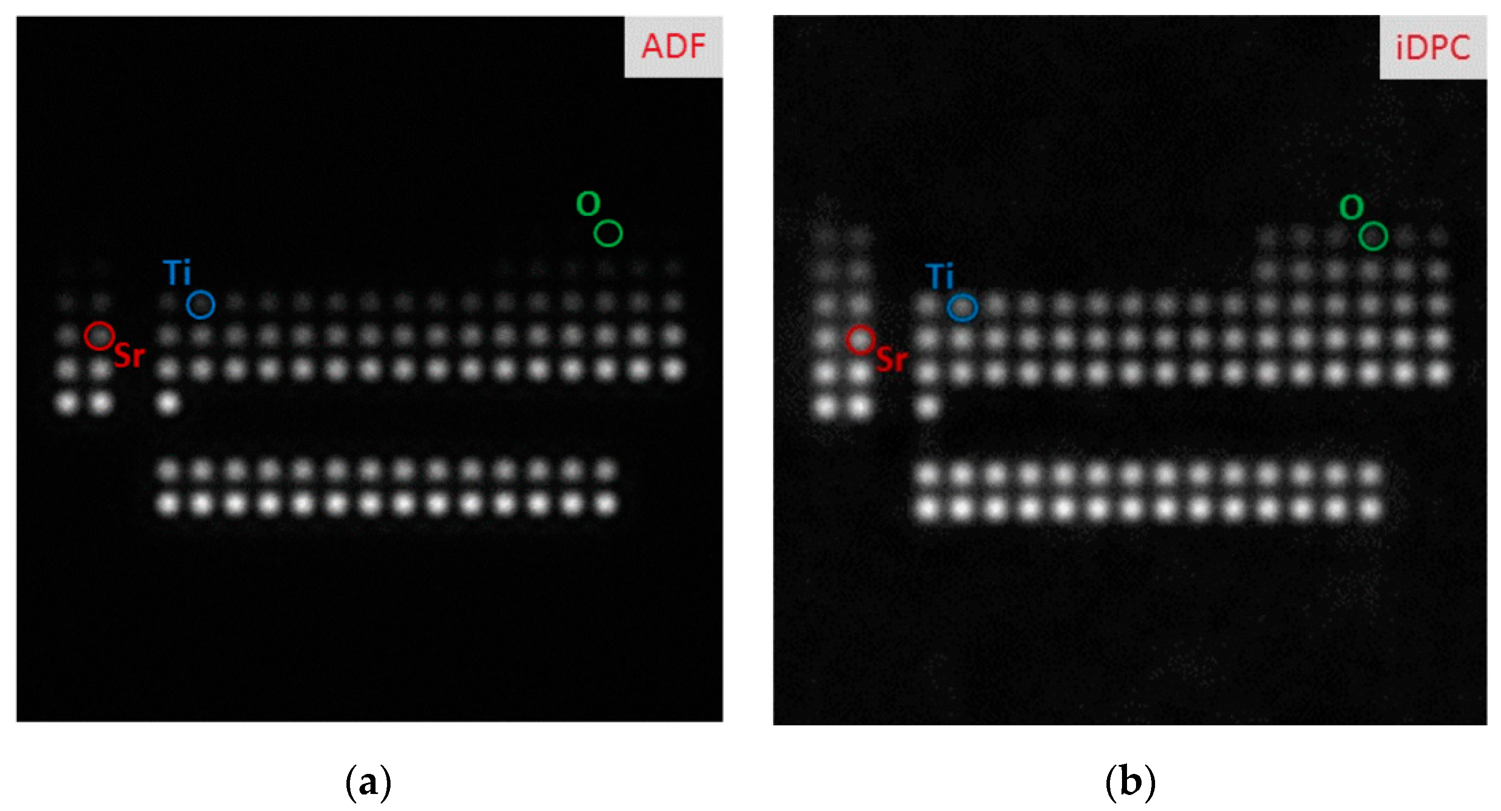
Enhancing imaging sensitivity is just as important as increasing the imaging resolution. Figure 5 compares the resolution of different elements using iDPC-STEM and HAADF-STEM. Both techniques are related to atomic number, and the contrast weakens upon decreasing the atomic number. However, comparing the element contrast of O, Ti, and Sr (circled in Figure 5) in the HAADF-STEM image, lighter elements are invisible or have reduced contrast, possibly below the noise level.
HAADF-STEM uses the high-angle scattered electrons to image, while iDPC-STEM uses atomic electrostatic potential [47,50] to directly image the phase. This difference in imaging principles, on the one hand, will lead to differences in image contrast: HAADF image contrast is approximately proportional to the square of the atomic number (Z1.6–2.0) [51], and iDPC image contrast is linearly related to the atomic number [46,52,53,54]; on the other hand, HAADF-STEM only uses high-angle scattered electrons, while iDPC-STEM, which uses almost all electrons for imaging, can obtain more signal at the same dose, thereby obtaining the characteristics that can be imaged at lower doses.
4.1. Advantages in Phase Contrast Imaging
Due to the use of atomic electrostatic potential to image the phase, iDPC-STEM has better sensitivity. The same goes for Electron Ptychography and 4D-STEM. Electron ptychography is a phase recovery method based on coherent diffraction imaging. The phase information of a sample is obtained through its diffraction pattern, and the phase contrast image of the sample is reconstructed.
The principle of 4D-STEM is shown in Figure 6a [55]. Based on the STEM mode, the annular electron detector is replaced by an array detector, and the entire diffraction pattern is recorded at each scanning position. Then, a camera with holes was developed to achieve simultaneous acquisition of EELS [56], as shown in Figure 6b. With the help of the 4D-STEM dataset, researchers can obtain the signal from any collection angle range, and various STEM images can be obtained through post-processing. Large data sets and complex post-processing are the main characteristics of the technique. By contrast, the several solid-state electron detectors (four in our case) employed by iDPC-STEM are two to three orders of magnitude faster than cameras used for electron ptychography and 4D STEM, especially without large data sets or cumbersome post-processing.
In this field, iDPC has obvious advantages and disadvantages: in terms of accuracy, electronic ptychography or iCOM-STEM can be used to obtain absolutely accurate the center of mass position information [46,47], while iDPC-STEM can only achieve the approximation of iCOM’s absolute accuracy by finer division (more partitions); in terms of imaging speed, iDPC has a much smaller amount of data processing: direct imaging, no huge reconstruction effort, a vast (orders of magnitude) speed advantage.
4.2. Advantages of Low-Dose Techniques
In the field of low-dose characterization, obtaining structural information of a series of electron-beam sensitive materials, such as zeolites [57,58,59,60,61,62,63], metal-organic frameworks [64,65,66,67,68,69,70], biomaterials [71,72,73,74,75,76], and some organic-inorganic hybrid materials is the main goal of the research. How to maintain a sufficient SNR of the image under low dose is the core issue of its development.
Figure 7 compares the capabilities of iDPC-STEM, HAADF-STEM, and K2 camera, which shows that iDPC-STEM has more comprehensive capabilities: in terms of imaging modes, STEM-based iDPC can obtain images that are easier to interpret, and the atomic number-related characteristics make it more capable of elemental resolution; the disadvantage is that the scanning time of a single image is long, which means that it is difficult to obtain real-time structures information and is susceptible to sample drift resulting in image distortion. In terms of data, iDPC technique does not have a huge dataset. In terms of equipment, iDPC technique only demands an additional four-section detector. Compared with K2 technique, which demands expensive cameras, iDPC technique has simpler equipment requirements and higher cost performance.
4.3. Advantages in Imaging Light Elements
Relevant structural information about light elements is often important. Nowadays, five main techniques are accessible to EM for imaging light atoms such as oxygen: low-angle annular dark field (LAADF-STEM), annular bright-field (ABF-STEM), integrated differential phase contrast (iDPC-STEM), negative Cs imaging (NCSI), and imaging STEM (ISTEM).
These techniques fall into three main categories. The first type is traditional STEM (sensitive to sample drift and scanning distortions), LAADF-STEM, ABF-STEM, and iDPC-STEM. The weak one here is LAADF-STEM, which is most optimal for mapping light atomic columns in very thin crystals only a few nanometers thick [77,78]. The second is based on a TEM imaging modality the image analysis process is complicated and often needs to be combined with simulations [79,80], and it is strongly dependent on aberrations and the sample thickness [79,81] The third one is convergent beam imaging combined with a CCD camera [82]. It is important to point out that imaging aberrations have a strong influence on the image and can even lead to contrast reversal. Probe aberrations have no influence whatsoever. (For additional details of the different techniques, please refer to the review [83]).
Their imaging principles and corresponding advantages and disadvantages are briefly summarized in Table 1. It can be seen that iDPC-STEM has certain universality and balance in the field of light element discrimination.
5. iDPC-STEM Application in Electron-Beam-Sensitive Materials
5.1. Application in Zeolites
Zeolites are widely used as acidic catalysts in the chemical and petrochemical industries due to their well-defined channels, high surface area, and tunable acidity [84,85,86,87,88,89,90,91,92,93,94]. Figure 8 shows statistics of published studies on zeolites in the past two decades. The overall trend is upward, and it displayed a faster upward trend from 2016 to 2020, which was related to the structural characterization of zeolites by iDPC-STEM. Although STEM images are easier to interpret than HR-TEM images, zeolite with radiolysis damage and electrostatic charging as the main damage mechanisms is more vulnerable to damage due to the instantaneous high intensity electron beam used in STEM. Therefore, HRTEM has been the main EM characterization method for many years. However, the ultra-low-dose properties of iDPC-STEM make the acquisition of high-resolution STEM images a reality.
ZSM-5 is a medium pore zeolite containing ten-membered rings. The framework is composed of two intersecting channel systems. The short axis is 5.1–5.2 Å; the other is a “Z”-shaped transverse channel with a nearly circular cross-section and a pore diameter of 5.4 ± 0.2 Å. Its unique microporous structure makes ZSM-5 have excellent shape selectivity and is a commonly used catalyst in the chemical field. ZSM-5 can be used in a variety of aromatization reactions, such as the methanol-to-aromatics process (MTA). The methanol-to-aromatics (MTA) process is important for converting coal/natural gas to chemicals [95]. Due to its poor electron beam stability, it is difficult to analyze its microstructure by transmission electron microscopy [96,97,98]. In 2016, its deactivation mechanism during the MTA reaction was explored by Prof. Wei’s group by low-dose iDPC-STEM [92]. Figure 9a is a schematic diagram of the catalytic process in MTA. Figure 9b,c is the low-dose HRTEM and iDPC-STEM images. It can be seen that the use of iDPC-STEM technique can achieve more precise characterization of the skeleton structure and explore the inside of the pore. This work has a great breakthrough in the EM characterization of ZSM-5. The results show that hydrothermal deactivation was mainly caused by the loss of frame-work acid sites and the blockage of channels by extra-framework alumina, provides theoretical guidance for further optimization of MTA process.
Due to the electron beam sensitivity of ZSM-5, it is difficult to distinguish whether the structural loss is caused by the reaction or the EM characterization. Figure 10a is an iDPC-STEM image of ZSM-5 along the <105> direction. Figure 10b is a magnified image in which the block units (Si-O islands) are bridged by only O atoms, and the O bridges can be clearly distinguished both in the image and the atomic model (in red and blue, respectively). The resolution was further confirmed by the strength profile analysis in Figure 10d. Figure 10e shows the atomically flat (010) surface with a half-channel termination structure. An enlarged atomic-scale surface structure is shown in the illustration, where even the Si-O dangling bonds on the surface can be directly observed. The results show that under the characterization condition, the atoms and dangling bonds on the surface did not undergo significant damage, which proved that iDPC-STEM can achieve the perfect structure characterization of such materials.
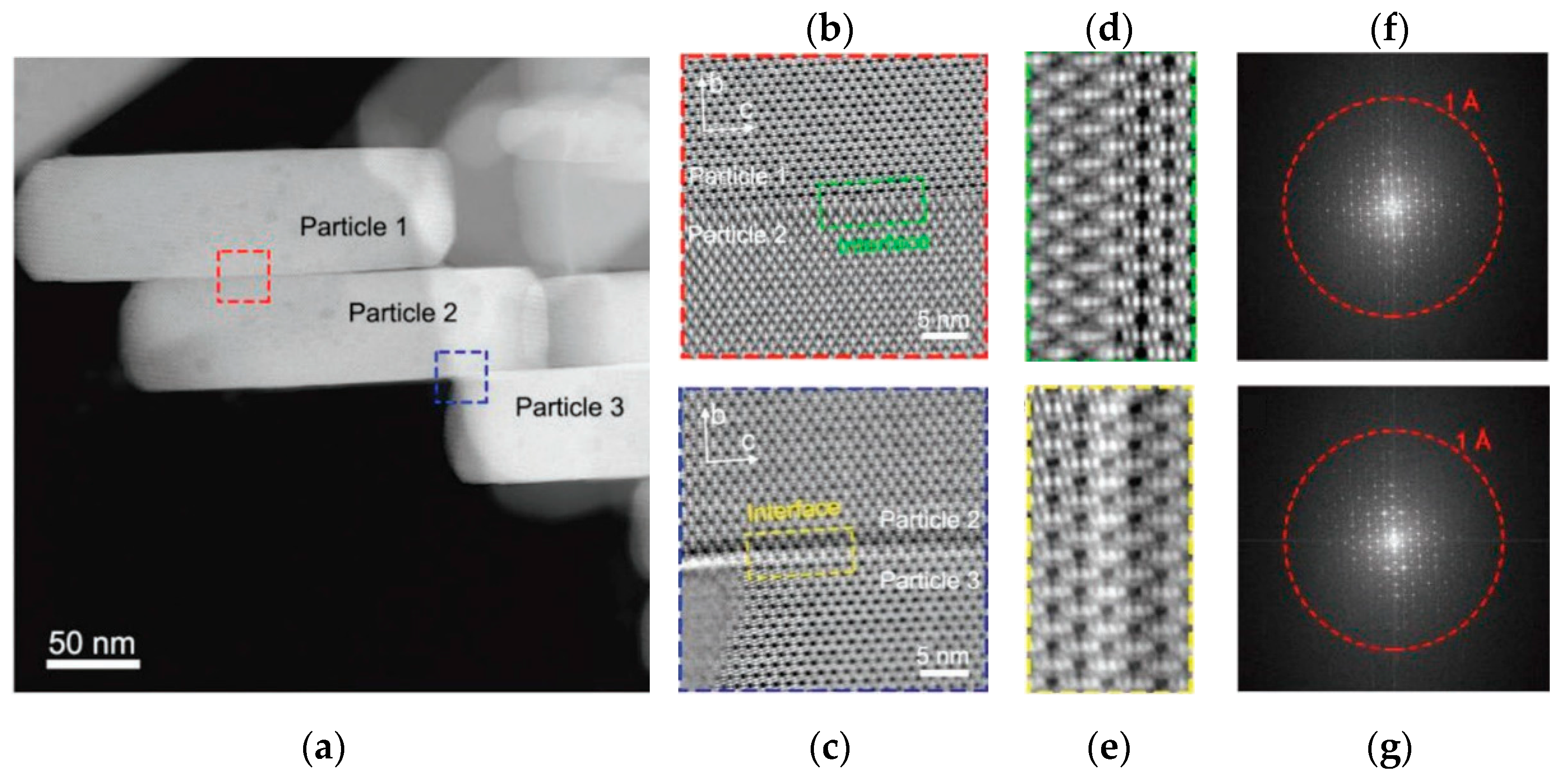
The iDPC-STEM technique can carry out the real structural characterization of the ZSM-5 structure, on this basis, the more in-depth study of the structure has been carried out. Figure 11a shows three particles of ZSM-5 that were closely connected by van der Waals interactions. Comparing the iDPC-STEM image at different scales (Figure 11b–e), the three particles showed completely consistent crystal orientation. The corresponding FFT patterns (Figure 11f,g) also exhibited a single-crystal-like nature with discrete diffraction spots. Such strict assembly and interfacial matching mean that the system must contain definite directional interaction, such as hydrogen bonds and hydroxyl groups. These will increase the transfer distance of guest molecules along the b-axis and ultimately affect the catalytic performance [94].
Figure 12a shows an iDPC-STEM image and its partial magnification of a Mo-ZSM-5 sample with a Si: Al ratio of 40 [99]. Previous studies have suggested a one-to-one correspondence between the Mo cluster and Al sites in zeolite frameworks when the Si/Al and Al/Mo ratios are proper [100,101] However, the correspondence was dubious due to the difficulty of real-space imaging and a lack of direct evidence. Now it is performed with iDPC-STEM. Figure 12b show zoomed-in areas (1, 2, and 3 of (a)): empty channel (Figure 12(bI)) and a channel containing a Mo cluster bound at the T8 site (Figure 12(bII)) and T1 site. (Figure 12(bIII)). According to simple statistics derived from 100 channels, Al most preferentially occupied the T1 site (40%), followed by T2 and T5 sites, and disfavored the T3 and T6 sites. The clear determination of the location of the acidic site (as the site of the catalytic reaction) is of great significance for the control of the catalytic behavior. In this work, iDPC-STEM was used to image the adsorbate in the pore to achieve the localization of the acidic site (aluminum) in the framework.
As shown in Figure 13 [102], a para-xylene (PX) molecule was used as a rotating pointer to detect the host-guest van der Waals interactions in the straight channel of the MFI-type zeolite framework. For a long time, single-molecule imaging was challenging but highly beneficial for investigating intermolecular interactions at the molecular level [103,104,105,106,107,108]. Now, with the help of iDPC-STEM, this has become a reality. In the iDPC-STEM image in Figure 13a, spindle-shaped spots can be clearly observed in some channels. The intensity profiles in Figure 13c also confirmed this. The spindle-shaped spots and the orientations of the PX molecules can be seen more clearly in the magnified image in Figure 13b. The agreement between the experimental and simulated results indicates that the C6-rings in the PX molecules have specific orientations, as expected in this van der Waals compass. This work achieved the direct imaging of a single molecule by iDPC-STEM to explore host-guest interactions in a range of organic-inorganic systems. This provides a new approach to studying the different behaviors of individual molecules.
Silicoaluminophosphate (SAPO) molecular sieves with small pores, such as SAPO-34 and SAPO-18, play an important catalytic role in methanol-to-olefin (MTO) reactions. Among them, molecular sieves with SAPO-18/SAPO-34 eutectic structure often show better performance than single molecular sieves in catalytic reactions due to the presence of both AEI and CHA structural units. However, due to the difficulty of electron microscopy characterization, SAPO-18 The /SAPO-34 eutectic structure is less studied. In Figure 14a–d, a local enlargement of an iDPC-STEM image of SAPO-18 (AEI) and SAPO-34 (CHA) from different orientations reveals the projection of the different bond lengths of Al-O and P-O bonds in different directions combined with their intensity profiles. This provides new possibilities for studying the symbiosis and accumulation of zeolite skeleton from the perspective of atoms and bonds. iDPC-STEM can also be used to analyze the surface atomic arrangement in thin regions. The red and blue arrows in Figure 14e indicate stacked AA or AB in SAPO-34/18 intergrowth catalyst surface. By comparing the top and bottom (Figure 14f,g), the stacking sequence was different at the top and bottom, which revealed the crystal growth trend [109].
In the field of zeolite, iDPC-STEM has achieved the characterization of fine structure. While providing real-space evidence that was difficult to obtain in the past, it has carried out a more in-depth analysis of the relationship between structure and catalyt-ic performance, which has a relatively complete and systematic study and has great development potential.
5.2. Application in MOFs
Metal-organic frameworks (MOFs) are typical porous materials constructed by orderly splicing organic linkers between metal nodes. Due to their designable topology, porosity, and functionality, they exhibit excellent performance for gas storage and separation, catalysis, drug delivery, and biomedical analysis [110,111]. Figure 15 shows a summary of the studies on MOFs in the past two decades, which shows a rapid upward trend.
MIL-101, the specific surface area is mostly above 4000 m2/g, and there is an effective inner diameter of about 2.9 nm and a window diameter of about 2.9 nm. Pentagonal holes with a diameter of about 1.2 nm and hexagonal holes with an effective inner diameter of about 3.4 nm and a window diameter of about 1.4 nm. MIL-101 is commonly used to support various metal atoms or active particles in catalysis research. Therefore, if the local structure of MIL-101 (the coordination relationship of nodes and linkers, etc.) can be imaged directly at the atomic scale, it would help understand the relationship between catalyst structure and performance [110,111]. Figure 16 shows the development of MIL-101 characterization techniques. In 2005, attempts were made to obtain low-dose HRTEM images with a certain signal-to-noise ratio. Only the main channels/cages could be distinguished [112]. In 2016, high-resolution HAADF-STEM images of heavy elements made it possible to identify the distribution of metal nodes and heavily-doped elements in MOFs [113]. In 2018, the camera was upgraded again (direct detection electron counting, DDEC). A higher detective quantum efficiency (DQE) enabled HRTEM to maintain an adequate signal-to-noise ratio at a sufficiently low electron beam dose [114]. In 2019, iDPC-STEM emerged for MOF characterization [115]. It can be seen from Figure. 16d that iDPC-STEM has a higher image contrast to the cage structure
In recent years, with the gradual popularization of iDPC-STEM, it has played an increasingly important role in the characterization of the surface, interface, and defects of MIL-101 and other non-periodic local structures [114]. Figure 17 shows the various surface structures of MIL-101 in iDPC-STEM images. This further proves the ability of iDPC-STEM in resolving cage structures.
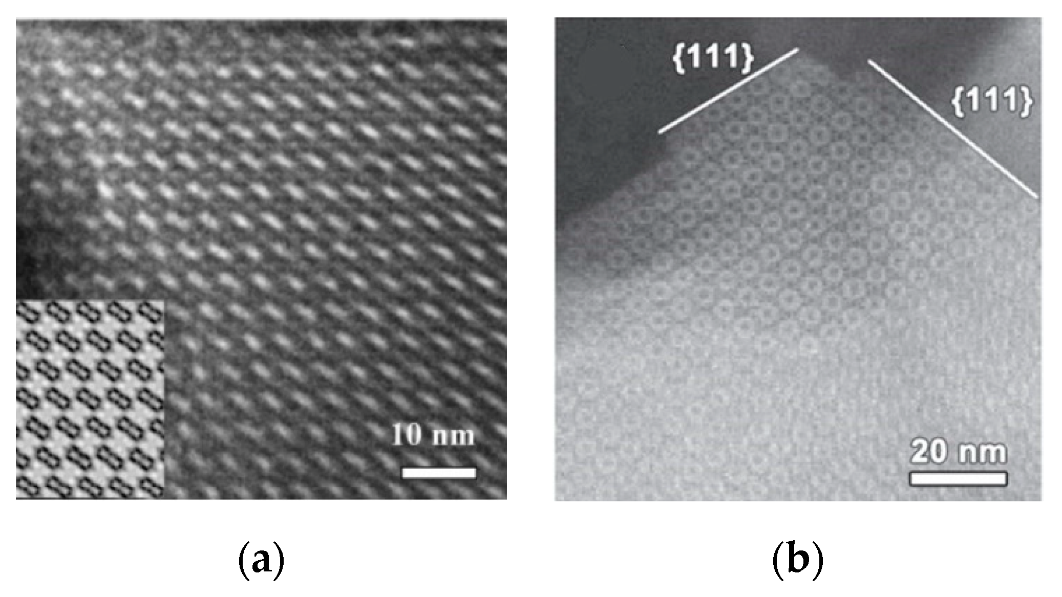
Figure 18 shows a study on the structural evolution characteristics of MIL-101 under electron beam radiation [116]. By collecting iDPC images from different cumulative electron beam doses, the evolution of the sample was analyzed. The results showed that the sample tended to shrink after irradiation. iDPC images with a resolution of 4.7 Å and good contrast for light elements can be used to quantitatively observe and analyze the local structural evolution of MIL-101 under electron beam irradiation. This work utilizes the high contrast of iDPC image for light elements to quantitatively observe and analyze the local structural evolution of MIL-101 under -electron beam irradiation.
In 2020, a study [117] (Figure 19) proposed a new strategy called “molecular compartments”, in which iDPC was used to identify the exact location of cage structures in TiO2-MIL-101 composites. The relative cage positions were obtained by HAADF-STEM (Figure 19a–c). The exact positions of TiO2 in MIl-101 cages were characterized by iDPC-STEM (Figure 19d–f), with a resolution of 3.2 Å. It is very important to accurately characterize the position of TiO2 in real space, and the catalytic effects of the compartments formed by TiO2 in different cage structures are also different. This work utilizes iDPC-STEM to achieve atomic structure imaging of different cage structures.
In the field of MOFs, more refined structural characterization has been achieved by iDPC-STEM, and related research on boundary, load and other types has also been carried out. Compared with the low-dose HRTEM images obtained with the k2 camera, it can be seen that iDPC-STEM has a huge advantage in image contrast, which enables it to identify cage structures more accurately.
5.3. Application in Perovskites
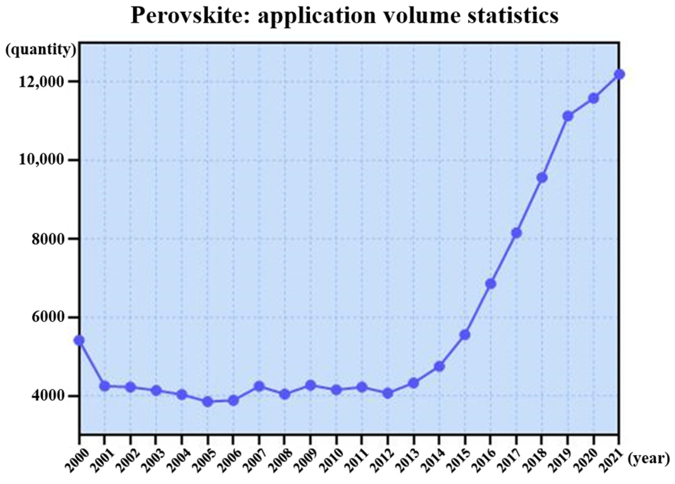
For the perovskite ABO3, the octahedral oxygen atoms surround a central B atom forming BO6, where the oxygen atoms affect various degrees of freedom (spin, orbit, charge) of the B atom and can give rise to new physical properties. To understand the physical properties more fully, it is necessary to describe the atomic space occupation, including the atomic-scale interface. Figure 20 summarizes studies on perovskites reported in the past two decades, which show the same rapid upward trend as the above materials.
Figure 21 shows a direct iDPC-STEM image of oxygen and cationic columns and follows their evolution with temperature in epitaxial Hf0.5Zr0.5O2(HZO)/La0.67Sr0.33MnO3 (LSMO and bottom electrode) heterostructures [118]. Figure 22 shows the oxygen positions in BaTiO3 obtained by iDPC-STEM, which are often difficult to identify [119]. The lower-left insets are magnified images selected from the white dotted box areas and show a schematic of BaTiO3.
Solar cells based on organic-inorganic hybrid perovskite materials (OIHPs) have developed rapidly due to their high photoelectric conversion efficiency. Over the past decade, their efficiencies have soared from 3.8% to 25.2%, almost matching that of monocrystalline silicon solar cells. However, their commercial applications are limited by the structural instability of hybrid perovskite materials, high temperature, oxygen, humid environment, light, and other factors that accelerate material decomposition. Therefore, it is necessary to deepen the understanding of degradation mechanisms to guide device design and material synthesis. As an electron-beam-sensitive material, studies have shown that the electron beam damage mechanism of OIHPs is irradiation decomposition, which is mainly affected by the dose. Therefore, iDPC-STEM will be of great help. However, most studies on its electron beam damage have focused on determining periodic structures by diffraction (Table 2). The application of iDPC-STEM in this field is relatively scarce, giving it large amounts of development potential
6. Summary and Outlook
Here, we have briefly introduced iDPC-STEM, an ideal tool for electron-beam-sensitive material characterization, including its development, imaging principles, and main applications. At present, iDPC-STEM has excellent characterization advantages for electron-beam-sensitive materials, but its further applications face some limitations.
Since its images rely on interactions between a focused electron beam and the electric field of a sample, it is demanding on both the beam and the detector, as with STEM. It is necessary to cooperate with the spherical aberration corrector to control the size of the beam to achieve a high resolution. For the detector, more continuous refinement partitions will bring it closer to iCOM imaging capabilities.
Due to its high contrast towards light elements, it is sensitive to sample surface contaminants, especially organic matter, and amorphous carbon. Therefore, there are requirements for sample preparation, storage, and electron microscope cleanliness.
Since its imaging process is based on weak phase approximation, for thin materials, high-quality images can be obtained; however, as the thickness of a sample increases, its contrast decreases. For samples of unknown thickness, such contrast changes make in-depth analysis difficult.
Due to its strong signal receiving efficiency, low-frequency noise may be amplified during integration. Therefore, to eliminate amplified noise, iDPC-STEM often chooses adaptive filtering techniques. The development of a suitable filtering technique is important for iDPC-STEM.
At present, the technique is still in its early development stages, and there are relatively few auxiliary tools (such as simulations), which need to be perfected.
In a word, although iDPC-STEM has excellent characterization advantages for electron beam sensitive materials, it has many limitations, especially for materials scientists with a weak background in electron microscopy, which greatly reduce its practical applications. The development direction of iDPC-STEM must be to constantly eliminate the above limitations and play a more important role.
Author Contributions
H.W., conceptualization, methodology, formal analysis, writing—original draft; L.L., conceptualization, writing—review and editing; J.W., conceptualization, investigation, writing—review and editing; C.L., conceptualization, investigation, writing—review and editing; J.H., conceptualization, investigation, writing—review and editing; K.Z., conceptualization, funding acquisition, writing—review and editing. All authors have read and agreed to the published version of the manuscript.
Funding
This work was supported by the National Natural Science Foundation of China (12074015), and the Beijing Outstanding Young Scientists Projects (BJJWZYJH01201910005018).
Institutional Review Board Statement
Not applicable.
Informed Consent Statement
Not applicable.
Data Availability Statement
Not applicable.
Acknowledgments
The authors are also grateful to Xianlin Qu; Hualei Yuan; Peijie Ma; Xu Zhang; Hanwen Hu, for their contribution to the work.
Conflicts of Interest
The authors declare no conflict of interest.
References
- Adams, C.J.; Haddow, M.F.; Lusi, M.; Orpen, A.G. Crystal engineering of lattice metrics of perhalometallate salts and MOFs. Proc. Natl. Acad. Sci. USA 2010, 107, 16033–16038. [Google Scholar] [CrossRef] [PubMed] [Green Version]
- Feyand, M.; Mugnaioli, E.; Vermoortele, F.; Bueken, B.; Dieterich, J.M.; Reimer, T.; Kolb, U.; De Vos, D.; Stock, N. Automated Diffraction Tomography for the Structure Elucidation of Twinned, Sub-micrometer Crystals of a Highly Porous, Catalytically Active Bismuth Metal-Organic Framework. Angew. Chem. Int. Ed. 2012, 51, 10373–10376. [Google Scholar] [CrossRef] [PubMed]
- Wu, H.; Chua, Y.S.; Krungleviciute, V.; Tyagi, M.; Chen, P.; Yildirim, T.; Zhou, W. Unusual and Highly Tunable Missing-Linker Defects in Zirconium Metal–Organic Framework UiO-66 and Their Important Effects on Gas Adsorption. J. Am. Chem. Soc. 2013, 135, 10525–10532. [Google Scholar] [CrossRef] [PubMed]
- Yakovenko, A.A.; Reibenspies, J.H.; Bhuvanesh, N.; Zhou, H.C. Generation and applications of structure envelopes for porous metal–Organic frameworks. J. Appl. Crystallogr. 2013, 46, 346–353. [Google Scholar] [CrossRef]
- Song, Q.; Nataraj, S.K.; Roussenova, M.V.; Tan, J.C.; Hughes, D.J.; Li, W.; Sivaniah, E. Zeolitic imidazolate framework (ZIF-8) based polymer nanocomposite membranes for gas separation. Energy Environ. Sci. 2012, 5, 8359–8369. [Google Scholar] [CrossRef]
- Fang, Z.; Bueken, B.; De Vos, D.E.; Fischer, R.A. Defect-Engineered Metal-Organic Frameworks. Angew. Chem. Int. Ed. 2015, 54, 7234–7254. [Google Scholar] [CrossRef] [Green Version]
- Makiura, R.; Motoyama, S.; Umemura, Y.; Yamanaka, H.; Sakata, O.; Kitagawa, H. Surface nano-architecture of a metal–Organic framework. Nat. Mater. 2010, 9, 565–571. [Google Scholar] [CrossRef]
- Rodenburg, J.M. Ptychography and Related Diffractive Imaging Methods. Adv. Imaging Electron Phys. 2008, 150, 87–184. [Google Scholar]
- Haider, M.; Rose, H.; Uhlemann, S.; Kabius, B.; Urban, K. Towards 0.1 nm resolution with the first spherically corrected transmission electron microscope. Microscopy 1998, 47, 395–405. [Google Scholar] [CrossRef]
- Rodenburg, J.M. Advances in Imaging and Electron Physics; Elsevier: Amsterdam, The Netherland, 2008; Volume 150, p. 87. [Google Scholar]
- Li, X.; Mooney, P.; Zheng, S.; Booth, C.R.; Braunfeld, M.B.; Gubbens, S.; Agard, D.A.; Cheng, Y. Electron counting and beam-induced motion correction enable near-atomic-resolution single-particle cryo-EM. Nat. Methods 2013, 10, 584–590. [Google Scholar] [CrossRef] [Green Version]
- Meyer, J.C.; Eder, F.; Kurasch, S.; Skakalova, V.; Kotakoski, J.; Park, H.J.; Kaiser, U. Accurate Measurement of Electron Beam Induced Displacement Cross Sections for Single-Layer Graphene. Phys. Rev. Lett. 2012, 108, 196102. [Google Scholar] [CrossRef] [PubMed]
- Greer, H.F.; Zhou, W. Electron diffraction and HRTEM imaging of beam-sensitive materials. Crystallogr. Rev. 2011, 17, 163–185. [Google Scholar] [CrossRef]
- Zhu, Y.; Ciston, J.; Zheng, B. Unravelling surface and interfacial structures of a metal–Organic framework by transmission electron microscopy. Nat. Mater. 2017, 16, 532–536. [Google Scholar] [CrossRef] [PubMed] [Green Version]
- Li, Y.; Wang, K.; Zhou, W. Cryo-EM Structures of Atomic Surfaces and Host-Guest Chemistry in Metal-Organic Frameworks. Matter 2019, 1, 428–438. [Google Scholar] [CrossRef] [PubMed] [Green Version]
- Zhang, D.; Zhu, Y.; Liu, L.; Ying, X.; Hsiung, C.E.; Sougrat, R.; Li, K.; Han, Y. Atomic-resolution transmission electron microscopy of electron beam–sensitive crystalline materials. Science 2018, 359, 675–679. [Google Scholar] [CrossRef] [Green Version]
- Liu, D.; Shadike, Z.; Lin, R.; Qian, K.; Li, H.; Li, K.; Li, B. Review of Recent Development of In Situ/Operando Characterization Techniques for Lithium Battery Research. Adv. Mater. 2019, 31, 1806620. [Google Scholar] [CrossRef]
- Fernandez-Leiro, R.; Scheres, S.H.W. Unravelling biological macromolecules with cryo-electron microscopy. Nature 2016, 537, 339–346. [Google Scholar] [CrossRef]
- Dubochet, J. On the Development of Electron Cryo-Microscopy (Nobel Lecture). Angew. Chem. Int. Ed. 2018, 57, 10842–10846. [Google Scholar] [CrossRef]
- Dubochet, J.; Knapek, E. Ups and downs in early electron cryo-microscopy. PLOS Biol. 2018, 16, e2005550. [Google Scholar] [CrossRef] [Green Version]
- Glaeser, R.M. Proteins, interfaces, and cryo-EM grids. Curr. Opin. Colloid Interface Sci. 2018, 34, 1–8. [Google Scholar] [CrossRef] [Green Version]
- Galaz-Montoya, J.G.; Ludtke, S.J. The advent of structural biology in situ by single particle cryo-electron tomography. Biophys. Rep. 2017, 3, 17–35. [Google Scholar] [CrossRef] [PubMed] [Green Version]
- Frank, J. Advances in the field of single-particle cryo-electron microscopy over the last decade. Nat. Protoc. 2017, 12, 209–212. [Google Scholar] [CrossRef] [PubMed]
- Bosch, E.G.T.; Lazic, I.; Lazar, S. Integrated Differential Phase Contrast (iDPC) STEM: A New Atomic Resolution STEM Technique To Image All Elements Across the Periodic Table. Microsc. Microanal. 2016, 22, 306–307. [Google Scholar] [CrossRef] [Green Version]
- Lazić, I.; Bosch, E.G.T.; Yucelen, R.; Imlau, R.; Sorin, L. Thick (3D) Sample Imaging Using iDPC-STEM at Atomic Scale. Microsc. Microanal. 2018, 24, 170–171. [Google Scholar] [CrossRef] [Green Version]
- Carlsson, A.; Alexandrou, I.; Yücelen, E. Low Dose Imaging Using Simultaneous iDPC- and ADF-STEM for Beam Sensitive Crystalline Structures. Microsc. Microanal. 2018, 24, 122–123. [Google Scholar] [CrossRef] [Green Version]
- Rose, H. Phase Contrast in Scanning Transmission Electron Microscopy. Optik 1974, 39, 416–436. [Google Scholar]
- Dekkers, N.H.; de Lang, H. Differential phase contrast in a STEM. Optik 1974, 41, 452–456. [Google Scholar]
- van Heel, A.C.S. Thickness Control of Thin Films. J. Opt. Soc. Am. 1957, 47, 483. [Google Scholar] [CrossRef]
- Waddell, E.M.; Chapman, J.N. Linear imaging of strong phase objects using asymmetric detectors in STEM. Optik 1979, 54, 83–96. [Google Scholar]
- Rose, H. Nonstandard imaging methods in electron microscopy. Ultramicroscopy 1976, 2, 251–267. [Google Scholar] [CrossRef]
- Chapman, J.N.; Batson, P.E.; Waddell, E.M.; Ferrier, R.P. The direct determination of magnetic domain wall profiles by differential phase contrast electron microscopy. Ultramicroscopy 1978, 3, 203–214. [Google Scholar] [CrossRef]
- Sannomiya, T.; Haga, Y.; Nakamura, Y.; Nittono, O.; Takahashi, Y. Observation of magnetic structures in Fe granular films by differential phase contrast scanning transmission electron microscopy. J. Appl. Phys. 2004, 95, 214–218. [Google Scholar] [CrossRef]
- Uhlig, T.; Zweck, J. Direct Observation of Switching Processes in Permalloy Rings with Lorentz Microscopy. Phys. Rev. Lett. 2004, 93, 47203. [Google Scholar] [CrossRef] [PubMed]
- Uhlig, T.; Rahm, M.; Dietrich, C.; Höllinger, R.; Heumann, M.; Weiss, D.; Zweck, J. Shifting and Pinning of a Magnetic Vortex Core in a Permalloy Dot by a Magnetic Field. Phys. Rev. Lett. 2005, 95, 237205. [Google Scholar] [CrossRef] [PubMed] [Green Version]
- Brownlie, C.; Mcvitie, S.; Chapman, J.N.; Wilkinson, C.D.W. Lorentz microscopy studies of domain wall trap structures. J. Appl. Phys. 2006, 100, 33902. [Google Scholar] [CrossRef]
- Sandweg, C.W.; Wiese, N.; Mcgrouther, D.; Hermsdoerfer, S.J.; Schultheiss, H.; Leven, B.; Mcvitie, S.; Hillebrands, B.; Chapman, J.N. Direct observation of domain wall structures in curved permalloy wires containing an antinotch. J. Appl. Phys. 2008, 103, 93906. [Google Scholar] [CrossRef] [Green Version]
- Hamilton, D.K.; Sheppard, C. Differential phase contrast in scanning optical microscopy. J. Microsc. 1984, 133, 27–39. [Google Scholar] [CrossRef]
- Shibata, N.; Kohno, Y.; Findlay, S.D.; Sawada, H.; Kondo, Y.; Ikuhara, Y. New area detector for atomic-resolution scanning transmission electron microscopy. J. Electron Microsc. 2010, 59, 473–479. [Google Scholar] [CrossRef]
- Lohr, M.; Schregle, R.; Jetter, M.; Wächter, C.; Wunderer, T.; Scholz, F.; Zweck, J. Differential phase contrast 2.0—Opening new “fields” for an established technique. Ultramicroscopy 2012, 117, 7–14. [Google Scholar] [CrossRef]
- Shibata, N.; Findlay, S.D.; Kohno, Y.; Sawada, H.; Kondo, Y.; Ikuhara, Y. Differential phase-contrast microscopy at atomic resolution. Nat. Phys. 2012, 8, 611–615. [Google Scholar] [CrossRef]
- Nellist, P.D. Atomic resolution comes into phase. Nat. Phys. 2012, 8, 586–587. [Google Scholar] [CrossRef]
- Müller, K.; Krause, F.F.; Béché, A.; Schowalter, M.; Galioit, V.; Löffler, S.; Verbeeck, J.; Zweck, J.; Schattschneider, P.; Rosenauer, A. Atomic electric fields revealed by a quantum mechanical approach to electron picodiffraction. Nat. Commun. 2014, 5, 5653. [Google Scholar] [CrossRef] [PubMed] [Green Version]
- Majert, S.; Kohl, H. High-resolution STEM imaging with a quadrant detector—Conditions for differential phase contrast microscopy in the weak phase object approximation. Ultramicroscopy 2015, 148, 81–86. [Google Scholar] [CrossRef] [PubMed]
- Lazic, I.; Bosch, E.; Lazar, S. Integrated differential phase contrast (iDPC) STEM. Acta Cryst. 2017, 73, C117–C118. [Google Scholar] [CrossRef] [Green Version]
- Lazić, I.; Bosch, E.G.T.; Lazar, S. Phase contrast STEM for thin samples: Integrated differential phase contrast. Ultramicroscopy 2016, 160, 265–280. [Google Scholar] [CrossRef]
- Lazić, I.; Bosch, E.G.T. Analytical Review of Direct Stem Imaging Techniques for Thin Samples. Adv. Imaging Electron Phys. 2017, 199, 75–184. [Google Scholar]
- Hawkes, P.W.; Kasper, E. Wave Optics; Academic Press Inc.: Cambridge, MA, USA, 1994; Volume 3. [Google Scholar]
- de Lang, H.; Dekkers, N.H. Microscope adapted for the generation of various contrast types: Theory and experiment. Appl. Opt. 1977, 16, 2215–2222. [Google Scholar] [CrossRef]
- Bosch, E.G.T.; Lazić, I. Analysis of HR-STEM theory for thin specimen. Ultramicroscopy 2015, 156, 59–72. [Google Scholar] [CrossRef]
- Krivanek, O.L.; Chisholm, M.F.; Nicolosi, V.; Pennycook, T.J.; Corbin, G.J.; Dellby, N.; Murfitt, M.F.; Own, C.S.; Szilagyi, Z.S.; Oxley, M.P.; et al. Atom-by-atom structural and chemical analysis by annular dark-field electron microscopy. Nature 2010, 464, 571–574. [Google Scholar] [CrossRef] [Green Version]
- Jiang, Y.; Chen, Z.; Han, Y.; Deb, P.; Gao, H.; Xie, S.; Purohit, P.; Tate, M.W.; Park, J.; Gruner, S.M.; et al. Electron ptychography of 2D materials to deep sub-ångström resolution. Nature 2018, 559, 343–349. [Google Scholar] [CrossRef]
- Chen, Z.; Jiang, Y.; Shao, Y.T.; Holtz, M.E.; Odstrcil, M.; Guizar-Sicairos, M.; Hanke, I.; Ganschow, S.; Schlom, D.G.; Muller, D.A. Electron ptychography achieves atomic-resolution limits set by lattice vibrations. Science 2021, 372, 826–831. [Google Scholar] [CrossRef] [PubMed]
- Yücelen, E.; Lazić, I.; Bosch, E.G.T. Phase contrast scanning transmission electron microscopy imaging of light and heavy atoms at the limit of contrast and resolution. Sci. Rep. 2018, 8, 2676. [Google Scholar] [CrossRef] [PubMed] [Green Version]
- Song, J.; Allen, C.S.; Gao, S.; Huang, C.; Sawada, H.; Pan, X.; Warner, J.; Wang, P.; Kirkland, A.I. Atomic Resolution Defocused Electron Ptychography at Low Dose with a Fast, Direct Electron Detector. Sci. Rep. 2019, 9, 1–8. [Google Scholar] [CrossRef] [PubMed] [Green Version]
- Song, B.; Ding, Z.; Allen, C.S.; Sawada, H.; Zhang, F.; Pan, X.; Warner, J.; Kirkland, A.I.; Wang, P. Hollow Electron Ptychographic Diffractive Imaging. Phys. Rev. Lett. 2018, 121, 146101. [Google Scholar] [CrossRef] [PubMed]
- Shen, K.; Wang, N.; Chen, X.; Chen, Z.; Li, Y.; Chen, J.; Qian, W.; Wei, F. Seed-induced and additive-free synthesis of oriented nanorod-assembled meso/macroporous zeolites: Toward efficient and cost-effective catalysts for the MTA reaction. Catal. Sci. Technol. 2017, 7, 5143–5153. [Google Scholar] [CrossRef]
- Mintova, S.; Olson, N.H.; Valtchev, V.P.; Bein, T. Mechanism of Zeolite A Nanocrystal Growth from Colloids at Room Temperature. Science 1999, 283, 958–960. [Google Scholar] [CrossRef]
- Wang, S.X.; Wang, L.M.; Ewing, R.C. Electron and ion irradiation of zeolites. J. Nucl. Mater. 2000, 278, 233–241. [Google Scholar] [CrossRef]
- Gu, B.X.; Wang, L.M.; Minc, L.D.; Ewing, R.C. Temperature effects on the radiation stability and ion exchange capacity of smectites. J. Nucl. Mater. 2001, 297, 345–354. [Google Scholar] [CrossRef]
- Esken, D.; Turner, S.; Lebedev, O.I.; Van Tendeloo, G.; Fischer, R.A. Au@ZIFs: Stabilization and Encapsulation of Cavity-Size Matching Gold Clusters inside Functionalized Zeolite Imidazolate Frameworks, ZIFs. Chem. Mater. 2010, 22, 6393–6401. [Google Scholar] [CrossRef]
- Lee, H.W.; Park, S.H.; Jeon, J.-K.; Ryoo, R.; Kim, W.; Suh, D.J.; Park, Y.-K. Upgrading of bio-oil derived from biomass constituents over hierarchical unilamellar mesoporous MFI nanosheets. Catal. Today 2014, 232, 119–126. [Google Scholar] [CrossRef]
- Malakootian, M.; Khatami, M.; Mahdizadeh, H.; Nasiri, A.; Amiri Gharaghani, M. A study on the photocatalytic degradation of p-Nitroaniline on glass plates by Thermo-Immobilized ZnO nanoparticle. Inorg. Nano-Met. Chem. 2019, 50, 124–135. [Google Scholar] [CrossRef]
- Wu, J.; Chen, J.; Wang, C.; Zhou, Y.; Ba, K.; Xu, H.; Bao, W.; Xu, X.; Carlsson, A.; Lazar, S.; et al. Metal–Organic Framework for Transparent Electronics. Adv. Sci. 2020, 7, 1903003. [Google Scholar] [CrossRef] [Green Version]
- Han, X.; Liu, P.; Lin, F.; Chen, W.; Luo, R.; Han, Q.; Jiang, Z.; Wang, X.; Song, S.; Reddy, K.M.; et al. Structures and Structural Evolution of Sublayer Surfaces of Metal–Organic Frameworks. Angew. Chem. Int. Ed. 2020, 59, 21419–21424. [Google Scholar] [CrossRef]
- Jiang, X.; Balsara, N.P. High-Resolution Imaging of Unstained Polymer Materials. ACS Appl. Polym. Mater. 2021, 3, 2849–2864. [Google Scholar] [CrossRef]
- Johnstone, D.N.; Firth, F.C.N.; Grey, C.P.; Midgley, P.A.; Cliffe, M.J.; Collins, S.M. Direct Imaging of Correlated Defect Nanodomains in a Metal–Organic Framework. J. Am. Chem. Soc. 2020, 142, 13081–13089. [Google Scholar] [CrossRef]
- Panda, J.; Sahoo, J.K.; Panda, P.K.; Sahu, S.N.; Samal, M.; Pattanayak, S.K.; Sahu, R. Adsorptive behavior of zeolitic imidazolate framework-8 towards anionic dye in aqueous media: Combined experimental and molecular docking study. J. Mol. Liq. 2019, 278, 536–545. [Google Scholar] [CrossRef]
- Liu, Y.; Liu, L.; Chen, X.; Liu, Y.; Han, Y.; Cui, Y. Single-Crystalline Ultrathin 2D Porous Nanosheets of Chiral Metal–Organic Frameworks. J. Am. Chem. Soc. 2021, 143, 3509–3518. [Google Scholar] [CrossRef]
- Liu, L.; Chen, Z.; Wang, J.; Zhang, D.; Zhu, Y.; Ling, S.; Huang, K.-W.; Belmabkhout, Y.; Adil, K.; Zhang, Y.; et al. Imaging defects and their evolution in a metal–organic framework at sub-unit-cell resolution. Nat. Chem. 2019, 11, 622–628. [Google Scholar] [CrossRef] [Green Version]
- Isa, L.; Lucas, F.; Wepf, R.; Reimhult, E. Measuring single-nanoparticle wetting properties by freeze-fracture shadow-casting cryo-scanning electron microscopy. Nat. Commun. 2011, 2, 1–9. [Google Scholar] [CrossRef]
- Sharp, T.H.; Bruning, M.; Mantell, J.; Sessions, R.B.; Thomson, A.R.; Zaccai, N.R.; Brady, R.L.; Verkade, P.; Woolfson, D.N. Cryo-transmission electron microscopy structure of a gigadalton peptide fiber of de novo design. Proc. Natl. Acad. Sci. USA 2012, 109, 13266–13271. [Google Scholar] [CrossRef] [Green Version]
- Kursula, I.; Cope, J.; Rank, K.C.; Gilbert, S.P.; Rayment, I.; Hoenger, A. Kar3Vik1 Uses a Minus-End Directed Powerstroke for Movement along Microtubules. PLoS ONE 2013, 8, e53792. [Google Scholar]
- Kopatz, I.; Zalk, R.; Levi-Kalisman, Y.; Zlotkin-Rivkin, E.; Frank, G.A.; Kler, S. Packaging of DNA origami in viral capsids. Nanoscale 2019, 11, 10160–10166. [Google Scholar] [CrossRef] [PubMed]
- Dalmônico, G.M.L.; López, E.O.; Longuinho, M.M.; Checca, N.R.; Farina, M.; Ersen, O.; Rossi, A.M.; Rossi, A.L. Insight by Cryo-TEM into the growth and crystallization processes of calcium phosphate nanoparticles in aqueous medium. Mater. Chem. Phys. 2019, 237, 121862. [Google Scholar] [CrossRef]
- Jokisaari, J.R.; Wang, C.; Qiao, Q.; Hu, X.; Reed, D.A.; Bleher, R.; Luan, X.; Klie, R.F.; Diekwisch, T.G.H. Particle-Attachment-Mediated and Matrix/Lattice-Guided Enamel Apatite Crystal Growth. ACS Nano 2019, 13, 3151–3161. [Google Scholar] [CrossRef] [PubMed]
- Gonnissen, J.; De Backer, A.; Den Dekker, A.J.; Martinez, G.T.; Rosenauer, A.; Sijbers, J.; Van Aert, S. Optimal experimental design for the detection of light atoms from high-resolution scanning transmission electron microscopy images. Appl. Phys. Lett. 2014, 105, 063116. [Google Scholar] [CrossRef] [Green Version]
- Gonnissen, J.; De Backer, A.; Den Dekker, A.J.; Sijbers, J.; Van Aert, S. Detecting and locating light atoms from high-resolution STEM images: The quest for a single optimal design. Ultramicroscopy 2016, 170, 128–138. [Google Scholar] [CrossRef] [Green Version]
- Jia, C.-L.; Lentzen, M.; Urban, K. High-Resolution Transmission Electron Microscopy Using Negative Spherical Aberration. Microsc. Microanal. 2004, 10, 174–184. [Google Scholar] [CrossRef] [Green Version]
- Urban, K.W.; Jia, C.-L.; Houben, L.; Lentzen, M.; Mi, S.-B.; Tillmann, K. Negative spherical aberration ultrahigh-resolution imaging in corrected transmission electron microscopy. Philos. Trans. R. Soc. A Math. Phys. Eng. Sci. 2009, 367, 3735–3753. [Google Scholar] [CrossRef]
- Lentzen, M.; Jahnen, B.; Jia, C.L.; Thust, A.; Tillmann, K.; Urban, K. High-Resolution Imaging with an Aberration-Corrected Transmission Electron Micrscope. Microsc. Microanal. 2001, 7, 904–905. [Google Scholar] [CrossRef]
- Rosenauer, A.; Krause, F.F.; Müller, K.; Schowalter, M.; Mehrtens, T. Conventional Transmission Electron Microscopy Imaging beyond the Diffraction and Information Limits. Phys. Rev. Lett. 2014, 113, 96101. [Google Scholar] [CrossRef]
- Gauquelin, N.; Van Den Bos, K.H.W.; Béché, A.; Krause, F.F.; Lobato, I.; Lazar, S.; Rosenauer, A.; Van Aert, S.; Verbeeck, J. Determining oxygen relaxations at an interface: A comparative study between transmission electron microscopy techniques. Ultramicroscopy 2017, 181, 178–190. [Google Scholar] [CrossRef] [PubMed]
- Olson, D.H.; Kototailo, G.T.; Lawton, S.L.; Meier, W.M. Crystal structure and structure-related properties of ZSM-5. J. Phys. Chem. B 1981, 85, 2238–2243. [Google Scholar] [CrossRef]
- Ono, Y. Transformation of Lower Alkanes into Aromatic Hydrocarbons over ZSM-5 Zeolites. Catal. Rev. 2006, 34, 179–226. [Google Scholar] [CrossRef]
- Conte, M.; Lopez-Sanchez, J.A.; He, Q.; Morgan, D.J.; Ryabenkova, Y.; Bartley, J.K.; Carley, A.F.; Taylor, S.H.; Kiely, C.J.; Khalid, K.; et al. Modified zeolite ZSM-5 for the methanol to aromatics reaction. Catal. Sci. Technol. 2012, 2, 105–112. [Google Scholar] [CrossRef]
- Ni, Y.; Sun, A.; Wu, X.; Hai, G.; Hu, J.; Li, T.; Li, G. The preparation of nano-sized H[Zn, Al]ZSM-5 zeolite and its application in the aromatization of methanol. Microporous Mesoporous Mater. 2011, 143, 435–442. [Google Scholar] [CrossRef]
- Shen, K.; Qian, W.; Wang, N.; Su, C.; Wei, F. Fabrication ofc-Axis Oriented ZSM-5 Hollow Fibers Based on an in Situ Solid–Solid Transformation Mechanism. J. Am. Chem. Soc. 2013, 135, 15322–15325. [Google Scholar] [CrossRef]
- Shen, K.; Qian, W.; Wang, N.; Zhang, J.; Wei, F. Direct synthesis of c-axis oriented ZSM-5 nanoneedles from acid-treated kaolin clay. J. Mater. Chem. A 2013, 1, 3272–3275. [Google Scholar] [CrossRef]
- Liu, Y.; Zhou, X.; Pang, X.; Jin, Y.; Meng, X.; Zheng, X.; Gao, X.; Xiao, F.-S. Improvedpara-Xylene Selectivity inmeta-Xylene Isomerization Over ZSM-5 Crystals with Relatively Longb-Axis Length. ChemCatChem 2013, 5, 1517–1523. [Google Scholar] [CrossRef]
- Ma, Y.; Wang, N.; Qian, W.; Wang, Y.; Zhang, J.; Wei, F. Molded MFI nanocrystals as a highly active catalyst in a methanol-to-aromatics process. RSC Adv. 2016, 6, 81198–81202. [Google Scholar] [CrossRef]
- Ma, Y.; Cai, D.; Li, Y.; Wang, N.; Muhammad, U.; Carlsson, A.; Tang, D.; Qian, W.; Wang, Y.; Su, D.; et al. The influence of straight pore blockage on the selectivity of methanol to aromatics in nanosized Zn/ZSM-5: An atomic Cs-corrected STEM analysis study. RSC Adv. 2016, 6, 74797–74801. [Google Scholar] [CrossRef]
- Cai, D.; Wang, N.; Chen, X.; Ma, Y.; Hou, Y.; Li, X.; Zhang, C.; Chen, Z.; Song, W.; Arslan, M.T.; et al. Highly selective conversion of methanol to propylene: Design of an MFI zeolite with selective blockage of (010) surfaces. Nanoscale 2019, 11, 8096–8101. [Google Scholar] [CrossRef] [PubMed] [Green Version]
- Shen, B.; Chen, X.; Cai, D.; Xiong, H.; Liu, X.; Meng, C.; Han, Y.; Wei, F. Atomic Spatial and Temporal Imaging of Local Structures and Light Elements inside Zeolite Frameworks. Adv. Mater. 2019, 32, 1906103. [Google Scholar] [CrossRef] [PubMed]
- Dimitrijevic, R.; Lutz, W.; Ritzmann, A. Hydrothermal stability of zeolites: Determination of extra-framework species of H-Y faujasite-type steamed zeolite. J. Phys. Chem. Solids 2006, 67, 1741–1748. [Google Scholar] [CrossRef]
- Chen, N.Y.; Mitchell, T.O.; Olson, D.H.; Pelrine, B.P. Irreversible Deactivation of Zeolite Fluid Cracking Catalyst. 2. Hydrothermal Stability of Catalysts Containing NH4Y and Rare Earth Y. Ind. Eng. Chem. Prod. Res. Dev. 1977, 16, 247–252. [Google Scholar] [CrossRef]
- Choi, M.; Na, K.; Kim, J.; Sakamoto, Y.; Terasaki, O.; Ryoo, R. Stable single-unit-cell nanosheets of zeolite MFI as active and long-lived catalysts. Nature 2009, 461, 246–249. [Google Scholar] [CrossRef] [PubMed]
- Vitolo, S.; Bresci, B.; Seggiani, M.; Gallo, M.G. Catalytic upgrading of pyrolytic oils over HZSM-5 zeolite: Behaviour of the catalyst when used in repeated upgrading–regenerating cycles. Fuel 2001, 80, 17–26. [Google Scholar] [CrossRef]
- Liu, L.; Wang, N.; Zhu, C.; Liu, X.; Zhu, Y.; Guo, P.; Alfilfil, L.; Dong, X.; Zhang, D.; Han, Y. Direct Imaging of Atomically Dispersed Molybdenum that Enables Location of Aluminum in the Framework of Zeolite ZSM-5. Angew. Chem. Int. Ed. 2020, 59, 819–825. [Google Scholar] [CrossRef]
- Ding, W.; Li, S.; Meitzner, G.D.; Iglesia, E. Methane Conversion to Aromatics on Mo/H-ZSM5: Structure of Molybdenum Species in Working Catalysts. J. Phys. Chem. B 2000, 105, 506–513. [Google Scholar] [CrossRef]
- Kosinov, N.; Coumans, F.J.a.G.; Uslamin, E.A.; Wijpkema, A.S.G.; Mezari, B.; Hensen, E.J.M. Methane Dehydroaromatization by Mo/HZSM-5: Mono- or Bifunctional Catalysis? ACS Catal. 2016, 7, 520–529. [Google Scholar] [CrossRef]
- Shen, B.; Chen, X.; Wang, H.; Xiong, H.; Bosch, E.G.T.; Lazić, I.; Cai, D.; Qian, W.; Jin, S.; Liu, X.; et al. A single-molecule van der Waals compass. Nature 2021, 592, 541–544. [Google Scholar] [CrossRef]
- Lee, H.J.; Ho, W. Single-Bond Formation and Characterization with a Scanning Tunneling Microscope. Science 1999, 286, 1719–1722. [Google Scholar] [CrossRef] [PubMed]
- Lantz, M.A.; Hug, H.J.; Hoffmann, R.; Van Schendel, P.J.A.; Kappenberger, P.; Martin, S.; Baratoff, A.; Guntherodt, H.J. Quantitative Measurement of Short-Range Chemical Bonding Forces. Science 2001, 291, 2580–2583. [Google Scholar] [CrossRef]
- Gross, L.; Mohn, F.; Moll, N.; Liljeroth, P.; Meyer, G. The Chemical Structure of a Molecule Resolved by Atomic Force Microscopy. Science 2009, 325, 1110–1114. [Google Scholar] [CrossRef] [Green Version]
- Albers, B.J.; Schwendemann, T.C.; Baykara, M.Z.; Pilet, N.; Liebmann, M.; Altman, E.I.; Schwarz, U.D. Three-dimensional imaging of short-range chemical forces with picometre resolution. Nat. Nanotechnol. 2009, 4, 307–310. [Google Scholar] [CrossRef] [PubMed]
- Gross, L.; Mohn, F.; Moll, N.; Meyer, G.; Ebel, R.; Abdel-Mageed, W.M.; Jaspars, M. Organic structure determination using atomic-resolution scanning probe microscopy. Nat. Chem. 2010, 2, 821–825. [Google Scholar] [CrossRef] [PubMed]
- Zhang, J.; Chen, P.; Yuan, B.; Ji, W.; Cheng, Z.; Qiu, X. Real-Space Identification of Intermolecular Bonding with Atomic Force Microscopy. Science 2013, 342, 611–614. [Google Scholar] [CrossRef] [PubMed] [Green Version]
- Shen, B.; Chen, X.; Fan, X.; Xiong, H.; Wang, H.; Qian, W.; Wang, Y.; Wei, F. Resolving atomic SAPO-34/18 intergrowth architectures for methanol conversion by identifying light atoms and bonds. Nat. Commun. 2021, 12, 1–9. [Google Scholar] [CrossRef]
- Ferey, G.; Mellot-Draznieks, C.; Serre, C.; Millange, F.; Dutour, J.; Surble, S.; Margiolaki, I. A Chromium Terephthalate-Based Solid with Unusually Large Pore Volumes and Surface Area. Science 2005, 309, 2040–2042. [Google Scholar] [CrossRef]
- Bhattacharjee, S.; Chen, C.; Ahn, W.-S. Chromium terephthalate metal–organic framework MIL-101: Synthesis, functionalization, and applications for adsorption and catalysis. RSC Adv. 2014, 4, 52500–52525. [Google Scholar] [CrossRef]
- Lebedev, O.I.; Millange, F.; Serre, C.; Ferey, G. First Direct Imaging of Giant Pores of the MetalOrganic Framework MIL-101. Chem. Mater. 2005, 17, 6525–6527. [Google Scholar] [CrossRef]
- Meledina, M.; Turner, S.; Filippousi, M.; Leus, K.; Lobato, I.; Ramachandran, R.K.; Dendooven, J.; Detavernier, C.; Van Der Voort, P.; Van Tendeloo, G. Direct Imaging of ALD Deposited Pt Nanoclusters inside the Giant Pores of MIL-101. Part. Part. Syst. Charact. 2016, 33, 382–387. [Google Scholar] [CrossRef]
- Li, X.; Wang, J.; Liu, X.; Liu, L.; Cha, D.; Zheng, X.; Yousef, A.A.; Song, K.; Zhu, Y.; Zhang, D.; et al. Direct Imaging of Tunable Crystal Surface Structures of MOF MIL-101 Using High-Resolution Electron Microscopy. J. Am. Chem. Soc. 2019, 141, 12021–12028. [Google Scholar] [CrossRef] [PubMed]
- Liu, L.; Zhang, D.; Zhu, Y.; Han, Y. Bulk and local structures of metal–organic frameworks unravelled by high-resolution electron microscopy. Commun. Chem. 2020, 3, 1–4. [Google Scholar] [CrossRef]
- Zhou, Y.; Xu, X.; Carlsson, A.; Lazar, S.; Pan, Z.; Ma, Y.; Terasaki, O.; Deng, H. Local Structure Evolvement in MOF Single Crystals Unveiled by Scanning Transmission Electron Microscopy. Chem. Mater. 2020, 32, 4966–4972. [Google Scholar] [CrossRef]
- Jiang, Z.; Xu, X.; Ma, Y.; Cho, H.S.; Ding, D.; Wang, C.; Wu, J.; Oleynikov, P.; Jia, M.; Cheng, J.; et al. Filling metal–organic framework mesopores with TiO2 for CO2 photoreduction. Nature 2020, 586, 549–554. [Google Scholar] [CrossRef]
- Nukala, P.; Ahmadi, M.; Antoja-Lleonart, J.; Graaf, S.D.; Wei, Y.; Zandbergen, H.W.; Kooi, B.J.; Noheda, B. In situ heating studies on temperature-induced phase transitions in epitaxial Hf0.5Zr0.5O2/La0.67Sr0.33MnO3 heterostructures. Appl. Phys. Lett. 2021, 118, 62901. [Google Scholar] [CrossRef]
- Jiang, H.; Qi, J.; Wu, D.; Lu, W.; Qian, J.; Qu, H.; Zhang, Y.; Liu, P.; Liu, X.; Chen, L. Atomic-resolution characterization on the structure of strontium doped barium titanate nanoparticles. Nano Res. 2021, 14, 4802–4807. [Google Scholar] [CrossRef]
- Chen, S.; Zhang, Y.; Zhang, X.; Zhao, J.; Zhao, Z.; Su, X.; Hua, Z.; Zhang, J.; Cao, J.; Feng, J.; et al. General Decomposition Pathway of Organic–Inorganic Hybrid Perovskites through an Intermediate Superstructure and its Suppression Mechanism. Adv. Mater. 2020, 32, 2001107. [Google Scholar] [CrossRef]
- Akhavan Kazemi, M.A.; Raval, P.; Cherednichekno, K.; Chotard, J.N.; Krishna, A.; Demortiere, A.; Reddy, G.N.M.; Sauvage, F. Molecular-Level Insight into Correlation between Surface Defects and Stability of Methylammonium Lead Halide Perovskite Under Controlled Humidity. Small Methods 2020, 5, 2000834. [Google Scholar] [CrossRef]
- Singh, R.K.; Kumar, R.; Jain, N.; Kuo, M.-T.; Upadhyaya, C.P.; Singh, J. Exploring the impact of the Pb2+ substitution by Cd2+ on the structural and morphological properties of CH3NH3PbI3 perovskite. Appl. Nanosci. 2019, 9, 1953–1962. [Google Scholar] [CrossRef]
- Yuan, Z.; Huang, W.; Ma, S.; Ouyang, G.; Hu, W.; Zhang, W. A high performance perovskite CH3NH3PbCl3 single crystal photodetector: Benefiting from an evolutionary preparation process. J. Mater. Chem. C 2019, 7, 5442–5450. [Google Scholar] [CrossRef]
- Balachandran, N.; Robert, T.M.; Jayalatha, T.; Neema, P.M.; Mathew, D.; Cyriac, J. Lead-free, mixed tin-copper perovskites with improved stability and optical properties. J. Alloys Compd. 2021, 879, 160325. [Google Scholar] [CrossRef]
- Chen, X.; Wang, Z. Investigating chemical and structural instabilities of lead halide perovskite induced by electron beam irradiation. Micron 2019, 116, 73–79. [Google Scholar] [CrossRef] [PubMed]
- Jayakrishnan, R.; Raj, A.; Varma, S.J. Self-assembled methyl-ammonium lead bromide thin films with blue photoluminescence. Appl. Nanosci. 2021, 11, 2095–2102. [Google Scholar] [CrossRef]
- Manekkathodi, A.; Marzouk, A.; Ponraj, J.; Belaidi, A.; Ashhab, S. Observation of Structural Phase Transitions and PbI2 Formation During the Degradation of Triple-Cation Double-Halide Perovskites. ACS Appl. Energy Mater. 2020, 3, 6302–6309. [Google Scholar] [CrossRef]
- Nie, L.; Ke, X.; Sui, M. Microstructural Study of Two-Dimensional Organic-Inorganic Hybrid Perovskite Nanosheet Degradation under Illumination. Nanomaterials 2019, 9, 722. [Google Scholar] [CrossRef] [Green Version]
- Navas, J.; Sánchez-Coronilla, A.; Gallardo, J.J.; Piñero, J.C.; De Los Santos, D.; Martín, E.I.; Hernández, N.C.; Alcántara, R.; Fernández-Lorenzo, C.; Martín-Calleja, J. The impact of Pd on the light harvesting in hybrid organic-inorganic perovskite for solar cells. Nano Energy 2017, 34, 141–154. [Google Scholar] [CrossRef]
- Rothmann, M.U.; Li, W.; Zhu, Y.; Bach, U.; Spiccia, L.; Etheridge, J.; Cheng, Y.-B. Direct observation of intrinsic twin domains in tetragonal CH3NH3PbI3. Nat. Commun. 2017, 8, 1–8. [Google Scholar] [CrossRef]
- Ge, Y.; Mu, X.; Lu, Y.; Sui, M. Photoinduced Degradation of Lead Halide Perovskite Thin Films in Air. Acta Phys. Chim. Sin. 2020, 36, 1905039–1905040. [Google Scholar] [CrossRef]
- Marí-Guaita, J.; Bouich, A.; Shafi, M.A.; Bouich, A.; Marí, B. Investigation on the Stability and Efficiency of MAPbI3 and MASnI3 Thin Films for Solar Cells. Phys. Status Solidi A 2022, 219, 2100364. [Google Scholar] [CrossRef]
- Yang, S.; Ke, X.; Chen, Q.; Huang, R.; Wang, W.; Wang, K.; Shu, K.; Tu, C.; Zheng, Z.; Luo, D.; et al. In-situ growth behavior of FAPbBr3 on two-dimensional materials for photocatalytic reaction to controllable products. J. Catal. 2021, 402, 143–153. [Google Scholar] [CrossRef]
- Xuan, Z.; Hao, X.; Qu, X.; Wang, Y.; Lai, H.; Chen, T.; Zhang, F.; Wang, W.; Zhao, D.; Wu, L.; et al. Efficient Perovskite Solar Cells with a Gradient Light Absorption Layer and Low VOC Loss Obtained by Interface Engineering. ACS Appl. Energy Mater. 2021, 4, 3584–3592. [Google Scholar] [CrossRef]
- Yuan, B.; Shi, E.; Liang, C.; Dou, L.; Yu, Y. Structural Damage of Two-Dimensional Organic–Inorganic Halide Perovskites. Inorganics 2020, 8, 13. [Google Scholar] [CrossRef] [Green Version]
- Zhu, Y.; Gui, Z.; Wang, Q.; Meng, F.; Feng, S.; Han, B.; Wang, P.; Huang, L.; Wang, H.-L.; Gu, M. Direct atomic scale characterization of the surface structure and planar defects in the organic-inorganic hybrid CH3NH3PbI3 by Cryo-TEM. Nano Energy 2020, 73, 104820. [Google Scholar] [CrossRef]
- Qin, F.; Wang, Z.; Wang, Z.L. Anomalous Growth and Coalescence Dynamics of Hybrid Perovskite Nanoparticles Observed by Liquid-Cell Transmission Electron Microscopy. ACS Nano 2016, 10, 9787–9793. [Google Scholar] [CrossRef]
- Song, K.; Liu, L.; Zhang, D.; Hautzinger, M.P.; Jin, S.; Han, Y. Atomic-Resolution Imaging of Halide Perovskites Using Electron Microscopy. Adv. Energy Mater. 2020, 10, 1904006. [Google Scholar] [CrossRef]
- Zhang, Q.; Zhao, J.; Xiao, Z.; Zhou, J.; Hong, B.; Luo, Z.; Bao, J.; Gao, C. Improved Moisture Stability of 2D Hybrid Perovskite (HOOC–CH2–NH3)2PbI4 by Dehydration Condensation between Organic Components. ACS Appl. Energy Mater. 2018, 1, 2502–2511. [Google Scholar] [CrossRef]
- Shi, E.; Yuan, B.; Shiring, S.B.; Gao, Y.; Akriti Guo, Y.; Su, C.; Lai, M.; Yang, P.; Kong, J.; Savoie, B.M.; et al. Two-dimensional halide perovskite lateral epitaxial heterostructures. Nature 2020, 580, 614–620. [Google Scholar] [CrossRef]
Figure 1.
The history of microscope development: more comprehensive and more realistic structural information is the current mainstream development direction.
Figure 1.
The history of microscope development: more comprehensive and more realistic structural information is the current mainstream development direction.

Figure 2.
High-energy electron beams will inevitably introduce damage while reducing structural information: knock on damage, radiolysis damage, electrostatic charging, and heating.
Figure 2.
High-energy electron beams will inevitably introduce damage while reducing structural information: knock on damage, radiolysis damage, electrostatic charging, and heating.

Figure 3.
Application status of iDPC-STEM in electron beam sensitive materials characterization.

Figure 4.
The schematic diagram of technical principle: partition probe, electrostatic potential imaging, and integral.
Figure 4.
The schematic diagram of technical principle: partition probe, electrostatic potential imaging, and integral.

Figure 5.
The comparison of single-atom contrast in the range Z = 1–103 obtained by simulations: HAADF-STEM image (a) and iDPC-STEM image (b) Reprinted/adapted with permission from Ref. [24]. Copyright 2016, Cambridge University Press.
Figure 5.
The comparison of single-atom contrast in the range Z = 1–103 obtained by simulations: HAADF-STEM image (a) and iDPC-STEM image (b) Reprinted/adapted with permission from Ref. [24]. Copyright 2016, Cambridge University Press.

Figure 6.
(a) Schematic diagram of the optical path of the 4D-STEM. Reprinted/adapted with permission from Ref. [55]. Copyright 2019, Springer Nature. (b) Based on the STEM mode, the ring-shaped electron detector is replaced by an arrayed detector, and the entire diffraction pattern is recorded at each scanning position Reprinted/adapted with permission from Ref. [56]. Copyright 2018, American Physical Society.

Figure 7.
The capability comparison of HAADF-STEM (a), iDPC-STEM (b) and K2 camera (c).

Figure 8.
The research quantity curve of zeolite in the past two decades.

Figure 9.
(a) MTA schematic; (b) HAADF-STEM of the synthesized ZSM-5; (c) iDPC-STEM Reprinted/adapted with permission from Ref. [92]. Copyright 2011, Royal Society of Chemistry.
Figure 9.
(a) MTA schematic; (b) HAADF-STEM of the synthesized ZSM-5; (c) iDPC-STEM Reprinted/adapted with permission from Ref. [92]. Copyright 2011, Royal Society of Chemistry.


Figure 10.
(a) The iDPC-STEM image of ZSM-5 from the <105> direction; (b–d) detailed analysis from (a); (e) the atomically flat (010) surface with clear Si-O dangling bonds. Reprinted/adapted with permission from Ref. [94]. Copyright 2019, Advanced Materials.
Figure 10.
(a) The iDPC-STEM image of ZSM-5 from the <105> direction; (b–d) detailed analysis from (a); (e) the atomically flat (010) surface with clear Si-O dangling bonds. Reprinted/adapted with permission from Ref. [94]. Copyright 2019, Advanced Materials.

Figure 11.
(a) The HAADF-STEM image of assembled ZSM-5 particles; (b,c) The iDPC-STEM images of the (010) interfaces in the areas marked in (a); (d,e) The zoom-in interface areas of iDPC-STEM images marked in (b,c); (f,g) The FFT patterns corresponding to (b) and (c), respectively. Reprinted/adapted with permission from Ref. [94]. Copyright 2019, Advanced Materials.

Figure 12.
(a) iDPC-STEM image of Mo/ZSM-5; (b) Zoomed-in areas 1 (I), 2 (II), and 3 (III) of (a) with an atomic model. Reprinted/adapted with permission from Ref. [99]. Copyright 2019, Angewandte Chemie.
Figure 12.
(a) iDPC-STEM image of Mo/ZSM-5; (b) Zoomed-in areas 1 (I), 2 (II), and 3 (III) of (a) with an atomic model. Reprinted/adapted with permission from Ref. [99]. Copyright 2019, Angewandte Chemie.

Figure 13.
(a,b) iDPC-STEM image (b, top), the structural model (b, middle) and the simulated image (b, bottom); (c) shows the corresponding intensity profile acquired from the red-framed region in (a).Reprinted/adapted with permission from Ref. [102]. Copyright 2021, Springer Nature.
Figure 13.
(a,b) iDPC-STEM image (b, top), the structural model (b, middle) and the simulated image (b, bottom); (c) shows the corresponding intensity profile acquired from the red-framed region in (a).Reprinted/adapted with permission from Ref. [102]. Copyright 2021, Springer Nature.

Figure 14.
(a–d) Magnified iDPC-STEM images with red box and intensity profiles (for red box) of SAPO-18 (a,c) and SAPO-34 (b,d)with blue box; (e) iDPC-STEM image of highly mixed SAPO-34 and SAPO-18 lattices inside; (f,g) iDPC-STEM images show the stacking sequences. Reprinted/adapted with permission from Ref. [109]. Copyright 2021, Applied Physics Letters.

Figure 15.
The research quantity curve of MOF in the past two decades.

Figure 16.
A series of electron microscopy images of MIL-101 acquired in different years: (a) HRTEM image in 2005. Reprinted/adapted with permission from Ref. [112]. Copyright 2005, American Chemical Society. (b) ADF-STEM image in 2016. Reprinted/adapted with permission from Ref. [113]. Copyright 2016, John Wiley and Sons. (c) low-dose HRTEM image (with DDEC) in 2019.(FFT for the white box) Reprinted/adapted with permission from Ref. [114]. Copyright 2019, American Chemical Society. (d) iDPC-STEM image in 2020. Reprinted/adapted with permission from Ref. [115]. Copyright 2020, Springer Nature.


Figure 17.
A series of electron microscopy images of the different surfaces in MIL-101: (a) The boundary includes most of the cage structure; (b) The boundary includes the whole of the cage structure; (c) The boundary includes few of the cage structure. And (i) HRETM; (ii) simulated image; (iii) structure model; (iv) iDPC-STEM. Reprinted/adapted with permission from Ref. [114]. Copyright 2019, American Chemical Society.

Figure 18.
(a) a series of iDPC-STEM images with the increased cumulative electron beam doses; (b–d) iDPC-STEM under different dose; (e,f) iDPC-STEM images before and after irradiation; (g,h) the corresponding FFT. Reprinted/adapted with permission from Ref. [116]. Copyright 2020, American Chemical Society.

Figure 19.
(a–c) A series of iDPC-STEM images with increased loading (TiO2); (d–f) Increased loading (TiO2) corresponding FFT. Red and blue outlines are overlaid on the images to highlight the positions of TiO2 units in separate types of mesopores. Scale bars: 5 nm. Reprinted/adapted with permission from Ref. [117]. Copyright 2020, Springer Nature.


Figure 20.
The research quantity of perovskites in the past two decades.

Figure 21.
(a) iDPC-STEM image of the LSMO layer in the virgin state; (b) is the enlarged image of the green box in (a). Reprinted/adapted with permission from Ref. [118]. Copyright 2021, AIP Publishing.
Figure 21.
(a) iDPC-STEM image of the LSMO layer in the virgin state; (b) is the enlarged image of the green box in (a). Reprinted/adapted with permission from Ref. [118]. Copyright 2021, AIP Publishing.

Figure 22.
(a) HAADFSTEM images of selected areas; (b) corresponding iDPC-STEM images. The white box is to highlight and magnify the structure. Reprinted/adapted with permission from Ref. [119]. Copyright 2021, Springer Nature.
Figure 22.
(a) HAADFSTEM images of selected areas; (b) corresponding iDPC-STEM images. The white box is to highlight and magnify the structure. Reprinted/adapted with permission from Ref. [119]. Copyright 2021, Springer Nature.


Table 1.
Comparison of five light-element imaging modes, including imaging mode, collection angles, and (dis)advantages.
Table 1.
Comparison of five light-element imaging modes, including imaging mode, collection angles, and (dis)advantages.
| Technique | Imaging Mode | Collection Angles | Advantage | Disadvantaged |
|---|---|---|---|---|
| LAADF | Convergence | α < θinner < 50 mrad | Light element imaging Lattice stress imaging | Sample drift and scan distortions |
| Affected by thickness | ||||
| Accuracy of light elements is insufficient | ||||
| ABF | Convergence | θinner = α/2, θouter = α | High resolution of light elements | Sample drift and scan distortions |
| Difficulty in distinguishing element types | ||||
| Invalid for weak phases | ||||
| iDPC | Convergence | 4 segment detectors | High resolution of light elements | Sample drift Scan distortions |
| NCSI | Parallel | CCD | No sample drifts Scan distortions High resolution of light elements | Accuracy of heavy elements is insufficient |
| strongly dependent on aberrations and the sample thickness | ||||
| Difficulty in interpretation | ||||
| iSTEM | Convergence | CCD | High resolution of light and heavy elements | Strongly dependent on aberrations and the sample thickness |
| Difficulty in interpretation |
Table 2.
Studies on MAPbI3 electron diffraction or fast Fourier transform patterns in the literature.
Table 2.
Studies on MAPbI3 electron diffraction or fast Fourier transform patterns in the literature.
| Specimen | Focus/Direction | Observation Method | Ref. |
|---|---|---|---|
| MAPbI3 and MAPbBr3 |
|
| [120] |
| MAPbI3 |
|
| [121] |
| MAPbI3 and MAPb0.9Cd0.1I3 |
|
| [122] |
| MAPbCl3 |
|
| [123] |
| MABr: SnBr2: CuCl21:1:0/1:0.5:0.5/1:0:1 |
|
| [124] |
| CsPbI3 and MAPbI3 |
|
| [125] |
| |||
| |||
| MAPbBr3 quantum dots |
|
| [126] |
| MAPbI3 |
|
| [127] |
| BA2PbBr4 |
|
| [128] |
| MAPb1−xPdxI3 x = 0.25, 0.5 |
|
| [129] |
| MAPbI3 |
|
| [130] |
| MAPbI3 |
|
| [131] |
| |||
| MAPbI3 and MASnI3 |
|
| [132] |
| FAPbBr3-WS2 and MoS2 |
|
| [133] |
| (CsPbI3)0.05((FAPbI3)1−x(MAPbBr3)x)0.95 |
|
| [134] |
| BA2FAPb2I7BA2MAPb2I7 |
|
| [135] |
| |||
| |||
| MAPbI3 |
|
| [136] |
| |||
| MAPbI3 |
|
| [137] |
| MAPbBr3 |
|
| [138] |
| MAPbBr3 |
|
| [139] |
| |||
| (2T)2PbI4-(2T)2PbBr4 |
|
| [140] |
Publisher’s Note: MDPI stays neutral with regard to jurisdictional claims in published maps and institutional affiliations. |
© 2022 by the authors. Licensee MDPI, Basel, Switzerland. This article is an open access article distributed under the terms and conditions of the Creative Commons Attribution (CC BY) license (https://creativecommons.org/licenses/by/4.0/).
Share and Cite
MDPI and ACS Style
Wang, H.; Liu, L.; Wang, J.; Li, C.; Hou, J.; Zheng, K. The Development of iDPC-STEM and Its Application in Electron Beam Sensitive Materials. Molecules 2022, 27, 3829. https://0-doi-org.brum.beds.ac.uk/10.3390/molecules27123829
AMA Style
Wang H, Liu L, Wang J, Li C, Hou J, Zheng K. The Development of iDPC-STEM and Its Application in Electron Beam Sensitive Materials. Molecules. 2022; 27(12):3829. https://0-doi-org.brum.beds.ac.uk/10.3390/molecules27123829
Chicago/Turabian StyleWang, Hongyi, Linlin Liu, Jiaxing Wang, Chen Li, Jixiang Hou, and Kun Zheng. 2022. "The Development of iDPC-STEM and Its Application in Electron Beam Sensitive Materials" Molecules 27, no. 12: 3829. https://0-doi-org.brum.beds.ac.uk/10.3390/molecules27123829