
Recent Developments on Rare-Earth Hexaboride Nanowires


1
School of Microelectronics, Southern University of Science and Technology, Shenzhen 518055, China
2
Department of Applied Physics, The Hong Kong Polytechnic University, Kowloon, Hong Kong 999077, China
*
Author to whom correspondence should be addressed.
Sustainability 2021, 13(24), 13970; https://0-doi-org.brum.beds.ac.uk/10.3390/su132413970
Submission received: 22 November 2021
/
Revised: 12 December 2021
/
Accepted: 14 December 2021
/
Published: 17 December 2021
(This article belongs to the Special Issue Advanced Semiconductor Materials for Energy, Electronics and Sensors)
Abstract
:With the rise of topological insulator samarium hexaboride (SmB6), rare-earth hexaboride (RB6) nanowires are the focus of the second wave of a research boom. Recent research has focused on new preparation methods, novel electronic properties, and extensive applications. Here, we review the recent developments in RB6 nanowires in the past five years. Two main synthesis methods (chemical vapor deposition and high-pressure solid-state) of RB6 nanowires are introduced and compared. Moreover, their electronic transport, magnetic properties, and superconducting properties are revealed. Furthermore, the applications of RB6 nanowires are presented, including as field emitters, photodetectors, and in energy storage. Finally, we detail further research directions for RB6 nanowires.
1. Introduction
Rare-earth hexaborides (RB6) have received substantial attention thanks to their high electrical conductivity, high melting points, and high chemical stability. Meanwhile, the strong correlation effect of 4f–5d electrons of rare-earth elements also brings some newfangled physical properties of RB6 [1,2,3]. For example, yttrium hexaboride (YB6) is a superconductor with a Tc of 7.2 K, which is the second highest transition temperature among all borides [4]. Moreover, lanthanum hexaboride (LaB6), possessing low work function of 2.7 eV, is a famous thermionic electron emission material with high current density and stability [5]. Cerium hexaboride (CeB6) is an antiferromagnetic heavy-fermion metal, but recently, it was found to demonstrate low-energy ferromagnetic fluctuation [6]. Furthermore, as a ferromagnetic semimetal, europium hexaboride (EuB6) recently exhibited a colossal magnetoresistance effect [7]. In recent years, the emergent topological insulator has increased interest in samarium hexaboride (SmB6), which possesses both insulating bulk state and metallic surface state due to the inversion of the d and f bands. Experimental evidence proves that SmB6 is the first strongly correlated 3D topological Kondo insulator [8].
Due to the small size effect and quantum confinement effect, one-dimensional (1D) nanomaterials have new properties compared with bulk crystals. With the rise of 1D nanomaterials, RB6 experienced the first wave of a research boom from 2005 to 2015, and many RB6 nanowires were prepared by chemical vapor deposition (CVD) [9,10,11,12,13,14,15,16,17,18,19,20]. These RB6 nanowires achieved excellent field emission properties and mechanical properties [21,22,23,24,25,26,27,28,29]. From 2016, the second wave of research boom of RB6 began as SmB6 proved to be a topological insulator, and researchers began to explore the difference in topological properties between nanowires and bulk single crystals [8].
In this review, we summarize the recent developments in RB6 nanowires. Two main synthesis methods of RB6 nanowires are summarized. Furthermore, their electronic transport and magnetic properties are summarized. Finally, the applications of RB6 nanowires are presented, including as field emitters, photodetectors, and in energy storage.
2. Growth of RB6 Nanowires
The structural models of rare-earth hexaborides are shown in Figure 1a. RB6 crystals are CsCl-type structures with a space group of Pm-3m. Among 17 rare-earth elements, only 13 can form hexaborides with boron, which are YB6, LaB6, CeB6, PrB6, NdB6, SmB6, EuB6, GdB6, TbB6, DyB6, HoB6, ErB6, and YbB6. On the left side of Figure 1a, one B6 octahedron is surrounded by eight R atoms, and RB6 crystals generally have suitable conductivity. On the right side of Figure 1a, one R atom is encircled by eight B6 octahedra, and B6 octahedra are connected by covalent bonds, which give RB6 high melting points, high hardness, and high chemical stability. From the study of electronic structure and bonding characteristics of LaB6, lanthanum and adjacent boron atoms are not sufficiently bonded, indicating that lanthanum atoms can migrate efficiently [30]. During the thermal field emission, the lanthanum atoms can freely migrate in the boron frame to replace the lanthanum atoms evaporated on the surface, thus showing excellent field emission performance [31]. Rare-earth hexaborides share common properties, but the special electronic structure of each material determines their characteristic properties. For instance, YbB6 was once proposed to be a topological insulator, but new evidence for the electronic structure suggests that its electronic states originate from the hybridization of the Yb d- and B p-orbits. This indicates that YbB6 has a non-topological insulator electronic structure [32]. Although most of the RB6 crystals are metals, SmB6 can open the band gap at low temperature due to the hybridization of the 4f bands and 5d bands, and meanwhile, metallic surface states are topologically protected [33]. To study and utilize the properties of RB6, high-quality crystals, especially low-dimensional nanowires, need to be prepared. Concerning materials preparation, only two methods are reported to obtain RB6 nanowires, chemical vapor deposition (CVD) and high-pressure solid-state (HPSS), as depicted in Figure 1b. CVD is a tradition method to grow RB6 nanowires using vapor–liquid–solid (VLS) or vapor–solid (VS) mechanisms at a high temperature. HPSS using autoclave is a new method to grow RB6 nanowires at a low temperature.
2.1. CVD Growth
In the past 5 years, a series of RB6 nanowires were prepared by the CVD method, namely, LaB6, CeB6, NdB6, SmB6, and ternary LaxPr1−xB6 nanowires, as shown in Figure 2. Different methods use different source materials and substrates, as summarized below.
RCl3 + B + B2O3 + H2 → RB6 (R = La, Sm)
From 2017 to 2019, Gan et al. used a Ni-catalyzed low-pressure CVD method to prepare high-quality LaB6 and SmB6 nanowires with a length of tens of microns, as depicted in Figure 2a [34,38]. The source materials of this method are LaCl3 (SmCl3), H2, B, and B2O3, and they are non-toxic. Halides are common rare-earth sources, easy to decompose and reactive. The innovation of this method lies in the use of B and B2O3 as the boron source, because boron powder alone is extremely difficult to change to a gaseous state and has low reactivity. At a high temperature of 1000 °C, the mixture of B and B2O3 can produce active B2O2 vapor, and then B2O2 reacts with LaCl3 (SmCl3) and H2 to grow LaB6 and SmB6 nanowires on Ni-coated Si substrates. The LaB6 nanowires exhibit excellent field emission properties and stability, both at room temperature and at high temperatures [34]. Compared with bulk single crystals, the transport properties prove that SmB6 nanowires have less residual resistance due to their large surface area [38].
CeCl3·7H2O + B2H6 → CeB6
In another method, Fu et al. applied a low-pressure CVD route to grow CeB6 nanowires on Au-coated flexible carbon cloths using CeCl3·7H2O and B2H6 as source materials, as depicted in Figure 2b [35]. In this method, the CeCl3·7H2O is safe, but the B2H6 gas is deleterious to humans. The field emission properties of flexible CeB6 nanowire arrays are outstanding, showing a low turn-on field and a high field emission enhancement factor. Meanwhile, the field current density can remain stable under bending conditions.
SmCl3 + BCl3 +H2 → SmB6
Besides B2H6 gas, BCl3 gas is also a common source of gaseous boron. In 2016, Zhou et al. used a CVD route to grow SmB6 nanowires on Au-coated Si substrates [39]. The electron transport testing on four-probe single-nanowire devices showed that the SmB6 nanowire has a saturated resistance under 10 K due to the presence of both insulating state in bulk and conductive state on the surface.
R + BCl3 + H2 → RB6 (R = Nd, LaxPr1−x)
In addition to the catalytic growth using metal particles (Au, Ni), there is also self-catalytic growth using rare-earth metals themselves as catalysts. In 2016, Han et al. reported the self-catalytic growth of NdB6 and ternary LaxPr1−xB6 nanowires by an ordinary-pressure CVD method, as shown in Figure 2c,d [36,37]. Besides the NdB6 nanowires, they also acquired NdB6 nanoawls and nanotubes. The growth of ternary LaxPr1−xB6 nanowires reveals that this self-catalytic method is suitable for doping and preparation of RB6 alloys.
2.2. HPSS Growth
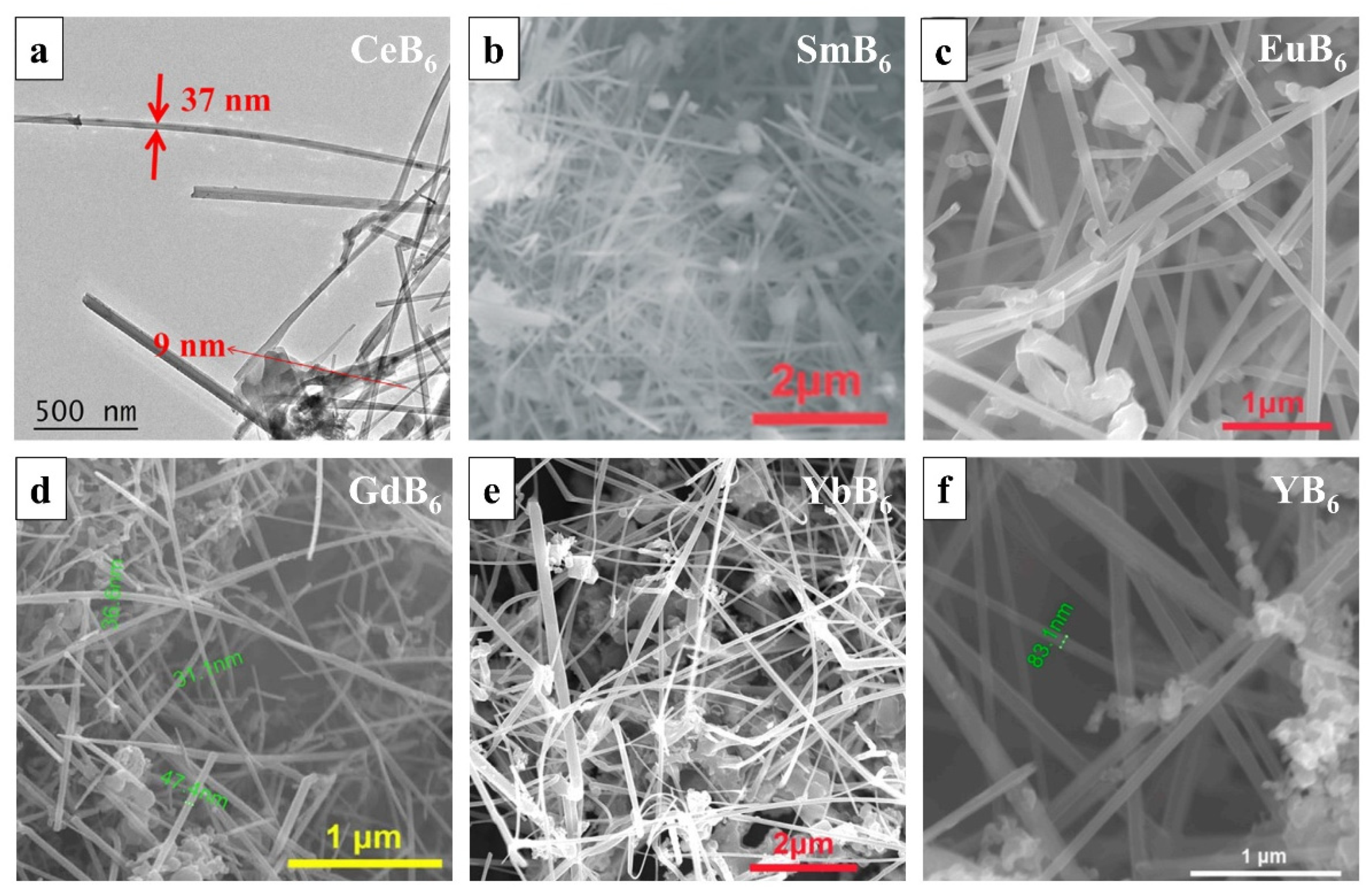
Along with the CVD route, the solid-state method is also a route to prepare RB6 crystals, including the high-pressure solid-state method [40,41,42,43,44,45,46,47], solution combustion method [48,49], and molten salt method [50,51]. However, because the diffusion rate of atoms in solid-state materials is extremely slow, it is difficult to obtain the nanowire morphology. At the same time, the low reactivity of solid source materials is also a problem restricting the development of 1D RB6 nanomaterials. To solve such problems, from 2016, Zhao group utilized a rare-earth metal, self-catalytic, high-pressure solid-state method (HPSS) route to prepare various RB6 nanowires, as shown in Figure 3a–f [52,53,54,55,56,57]. It is noteworthy that, until now, this is the only report on the synthesis of YbB6 nanowires [56]. The general chemical reaction of the HPSS method is given below.
R + 6 H3BO3 + 10 Mg + I2 → RB6 + 9 MgO + MgI2 + 9 H2O
In this equation, Mg is used for the reduction of H3BO3, and I2 acts as the catalyst to boost the reaction of R and B atoms. From the literature, the Gibbs free energy (ΔrG) and heat function (ΔrH) of this equation are about −1900 kJ mol−1 and −2000 kJ mol−1, respectively, demonstrating that the reaction is spontaneous and exothermic. Moreover, the high pressure in the autoclave is generated by iodine (higher than 45 atm), which is also a key to obtaining RB6 nanowires. Due to high exothermic and high pressure, the trigger temperature of this HPSS method (200–260 °C) is generally much lower than that of the CVD method (950–1100 °C). From the ex situ time-dependent morphology study (5 min, 30 min, 360 min), we speculate that the growth of nanowires has three steps: (i) diffusion and reaction of R and B atoms; (ii) nucleation of RB6 crystals; (iii) growth of RB6 nanowires [53]. This HPSS route is a general method for the synthesis of rare-earth hexaborides, which we believe can be extended to the synthesis of other metal boride nanowires.
3. Properties and Applications of RB6 Nanowires
3.1. Electronic Transportation
As an emerging topological insulator, many experiments and theoretical studies have been conducted on bulk SmB6 single crystals [8]. From 2016, researchers began to investigate the novel electronic transport and magneto-transport properties of SmB6 nanowires [37,38,53,58,59,60,61,62]. In 2017, Kong et al. reported the spin-polarized surface state transport of single SmB6 nanowires (Figure 4a–c) [58]. Under 5 K, the resistance appears saturated and flat, indicating that the surface states control the transport behavior. The appearance of topological surface states is caused by the reversal of d and f electrons. The fitting of a temperature-dependent resistance curve reveals that SmB6 nanowire has a bulk gap ~3.2 meV, which is opened by the hybridization of the 4f bands and 5d bands in SmB6 nanowires. As shown in Figure 4c, the magnetoresistance (MR) of SmB6 nanowires is negative and the MR shows no sign of saturation at high magnetic field up to 14 T. The negative MR indicates that this transport behavior is spin-dependent. Furthermore, the nonlocal tests reveal that the surface state transport of SmB6 nanowires is spin-polarized. In another interesting work, Zhou et al. reported the positive planar Hall effect (PHE) of SmB6 nanowires (Figure 4d–f) [59]. They found that as the temperature decreases, the amplitude increases sharply, but saturates at 5 K. This positive PHE is due to the surface states of SmB6. In other studies, the researchers found the anomalous magnetoresistance and the hysteresis of magnetoresistance in SmB6 nanowires [60,61,62].
In the RB6 family, like SmB6, YbB6 is proposed to be a mixed-valent (Yb2+/Yb3+) topological insulator and demonstrates new quantum phenomena [63,64,65]. In 2018, Han et al. reported the semiconductor–insulator transition behavior in a YbB6 nanowire (Figure 5) [55]. As shown in Figure 5b, as the temperature decreases from 300 to 2 K, the resistivity of the YbB6 nanowire device undergoes a dramatic 49-fold increase (ρ2 K/ρ300 K = 49). They propose that the semiconductor–insulator transition is due to a small band gap opening at a low temperature induced by the slightly boron-rich or boron-deficient segments in YbB6 nanowires. Furthermore, the magnetoresistance (MR) of the YbB6 nanowire was tested with perpendicular magnetic field B = 0–7 T at various temperatures. As displayed in Figure 5c, the MR shows no sign of saturation at high magnetic field up to 14 T and has a linear dependence with B2 at 2 K and 10 K, which follows Kohler’s law. Because a semiconductor–insulator transition occurred at 2 K for YbB6 nanowires, the hole-dominant transport is credible at 2 K and the transport at 10 K is electron-dominant.
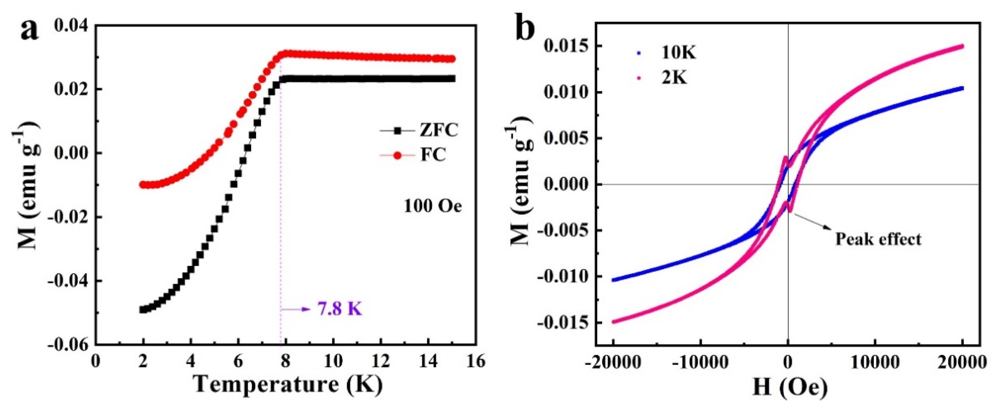
Of all the metal borides, YB6 bulk crystals have the second highest superconducting transition temperature of 7.2 K after MgB2. More superconducting properties have been studied in bulk YB6 single crystals, but the superconducting properties of YB6 nanowires have not been reported. Recently, Wang et al. reported the synthesis of 1D YB6 nanowires by a high-pressure solid-state method and studied their magnetic properties (Figure 6). The temperature-dependent magnetization under zero-field cooling and field cooling revealed that the YB6 nanowires have a superconducting transition with Tc = 7.8 K. Meanwhile, they found that the YB6 nanowires exhibited a peak effect in the superconducting state observed from the magnetic hysteresis loops obtained at 2 K and 10 K, indicating that YB6 nanowires pertain to a type-II superconductor.
LaB6 bulk single crystals have been applied in commercial scanning electron microscopy and transmission electron microscopy. For RB6 nanowires, the most attractive application is also the field emitter of an electronic gun of an electron microscope (Figure 7) [66,67,68]. Published in Nature Nanotechnology, Zhang et al. reported the first application of a single LaB6 nanowire to scanning electron microscopy, revealing excellent performance [66]. Their LaB6 nanowire electron source shows low work function, is chemically inert, and has high monochromaticity. When assembled into a field-emission gun of SEM, it demonstrates ultra-low emission decay, and its current density gain is three orders of magnitude higher than traditional W tips. By this LaB6 nanowire-based SEM, they obtained low-noise and high-resolution images, better than W-tip-based SEM. Recently, published in Nature Nanotechnology in 2021, Zhang et al. reported the installation of a single LaB6 nanowire into an aberration-corrected transmission electron microscope [67]. The LaB6 NW-based TEM achieved atomic resolution and probe-forming modes at 60 kV energy. Compared with the state-of-the-art W (310) electron source, the nanostructured electron source provides higher temporal coherence at a spatial frequency of 105 pm, showing a higher contrast transfer amplitude of 84% and a spectral energy resolution of 35%. The first demonstration of the LaB6 nanowire electron source in SEM and TEM reveals that the RB6 nanowires have notable application prospects and commercial value both in electron microscopy and other electron-emitting devices.
3.2. Optoelectronic Properties
Most of the RB6 crystals are metals with zero band gap, and thus, they are not suitable for semiconductor devices, such as field effect transistors and photodetectors. However, as a topological Kondo insulator, SmB6 shows a small gap (3 meV), evidenced by electrical transport measurements, and may have potential in fabricating devices. Recently, Zhou et al. [69] first reported the self-powered SmB6 nanowire photodetectors with broadband wavelengths covering from 488 nm to 10.6 μm (Figure 8). They claimed that the photocurrent stemmed from the interface of SmB6 nanowire and Au electrodes owing to the built-in potential, proved by the spatially resolved photocurrent mapping. The current on/off ratio, responsibility, and specific detectivity are 100, 1.99 mA/W, and 2.5 × 10⁷ Jones, respectively. The demonstration of a SmB6 nanowire photodetector reveals its application potential in mid-infrared photodetectors.
3.3. Electrochemical Performances
RB6 crystals show excellent metal-like conductivity (>103 S m−1) and they are suitable for active electrochemical electrode materials for energy storage. Recently, Wang et al. [52] reported the application of CeB6 nanowires as lithium-ion battery anode materials, and they obtained a capacity of ~225 mA h g−1 after 60 cycles (Figure 9a). The kinetic analysis shows that the Li+ storage mechanism mainly comes from the surface capacitive behavior. Xue et al. [70] reported the LaB6 nanowires on carbon fiber as electrode materials for supercapacitors (Figure 9b). The LaB6 electrode materials showed a high areal capacitance of 17.34 mF cm−2 and revealed suitable cycling stability after 10,000 cycles. The successful application of RB6 nanowires in batteries and capacitors demonstrates their potential in the field of electrochemical energy storage.
4. Conclusions and Outlook
In conclusion, we review in this paper the recent developments in RB6 nanowires in the past five years. Two main synthesis methods (CVD and HPSS) of RB6 nanowires are outlined and compared. Moreover, their electronic transport, magnetic properties, and superconducting properties are summarized. Finally, the applications of RB6 nanowires are revealed, including as field electron emitters, photodetectors, and in energy storage.
With the rise of two-dimensional (2D) materials, RB6 nanowires should absorb some of the advantages of 2D material, such as atomically thin and large area lateral size. If RB6 nanowires become thinner and wider, also called RB6 nanobelts, they may reveal novel properties (Figure 10). In a recent study, Lee et al. reported the perfect Andreev reflection in a topological superconducting state based on SmB6/YB6 heterostructures [71]. We believe the heterostructures based on combinations of RB6 nanowires or films may find new physical phenomena and represent future trends. In terms of the synthesis methods, CVD, solid-state, MBE, and PLD methods are all applicable, and only few improvements are needed. For instance, when using the CVD method to grow RB6 nanobelts, mica substrates may be the best. Furthermore, adding some salts can improve the growth efficiency [72]. Meanwhile, 2D rare-earth materials have shown novel properties and applications, and thus, new discoveries and properties will also arise regarding the atomically thin 2D RB6 nanobelts.
Author Contributions
Writing—original draft preparation, Z.W., W.H.; writing—review and editing, Z.W., W.H.; supervision, W.H.; funding acquisition, W.H. All authors have read and agreed to the published version of the manuscript.
Funding
This research was funded by National Natural Science Foundation Committee of China (grant number 22105162).
Acknowledgments
The authors thank the grant from National Natural Science Foundation Committee of China (grant number 22105162).
Conflicts of Interest
The authors declare no conflict of interest.
References
- Ji, X.H.; Zhang, Q.Y.; Xu, J.Q.; Zhao, Y.M. Rare-earth hexaborides nanostructures: Recent advances in materials, characterization and investigations of physical properties. Prog. Solid State Chem. 2011, 39, 51–69. [Google Scholar] [CrossRef]
- Carenco, S.; Portehault, D.; Boissiere, C.; Mezailles, N.; Sanchez, C. Nanoscaled metal borides and phosphides: Recent developments and perspectives. Chem. Rev. 2013, 113, 7981–8065. [Google Scholar] [CrossRef] [PubMed]
- Gan, H.; Zhang, T.; Guo, Z.; Lin, H.; Li, Z.; Chen, H.; Chen, J.; Liu, F. The growth methods and field emission studies of low-dimensional boron-based nanostructures. Appl. Sci. 2019, 9, 1019. [Google Scholar] [CrossRef] [Green Version]
- Kunii, S.; Kasuya, T.; Kadowaki, K.; Date, M.; Woods, S.B. Electron tunneling into superconducting YB6. Solid State Commun. 1984, 52, 659–661. [Google Scholar] [CrossRef]
- Zhang, H.; Tang, J.; Zhang, Q.; Zhao, G.; Yang, G.; Zhang, J.; Zhou, O.; Qin, L.-C. Field emission of electrons from single LaB6 nanowire. Adv. Mater. 2006, 18, 87–91. [Google Scholar] [CrossRef]
- Jang, H.; Friemel, G.; Ollivier, J.; Dukhnenko, A.V.; Shitsevalova, N.Y.; Filipov, V.B.; Keimer, B.; Inosov, D.S. Intense low-energy ferromagnetic fluctuations in the antiferromagnetic heavy-fermion metal CeB6. Nat. Mater. 2014, 13, 682–687. [Google Scholar] [CrossRef] [Green Version]
- Pohlit, M.; Rößler, S.; Ohno, Y.; Ohno, H.; Von Molnár, S.; Fisk, Z.; Müller, J.; Wirth, S. Evidence for ferromagnetic clusters in the colossal-magnetoresistance material EuB6. Phys. Rev. Lett. 2018, 120, 257201. [Google Scholar] [CrossRef] [PubMed]
- Li, L.; Sun, K.; Kurdak, C.; Allen, J.W. Emergent mystery in the Kondo insulator samarium hexaboride. Nat. Rev. Phys. 2020, 2, 463–479. [Google Scholar] [CrossRef]
- Zhang, H.; Zhang, Q.; Tang, J.; Qin, L.C. Single-crystalline LaB6 nanowires. J. Am. Chem. Soc. 2005, 127, 2862–2863. [Google Scholar] [CrossRef]
- Zhang, H.; Zhang, Q.; Tang, J.; Qin, L.C. Single-crystalline CeB6 nanowires. J. Am. Chem. Soc. 2005, 127, 8002–8003. [Google Scholar] [CrossRef]
- Zhang, H.; Zhang, Q.; Zhao, G.; Tang, J.; Zhou, O.; Qin, L.C. Single-crystalline GdB6 nanowire field emitters. J. Am. Chem. Soc. 2005, 127, 13120–13121. [Google Scholar] [CrossRef]
- Xu, J.; Zhao, Y.; Zou, C. Self-catalyst growth of LaB6 nanowires and nanotubes. Chem. Phys. Lett. 2006, 423, 138–142. [Google Scholar] [CrossRef]
- Zou, C.Y.; Zhao, Y.M.; Xu, J.Q. Synthesis of single-crystalline CeB6 nanowires. J. Cryst. Growth 2006, 291, 112–116. [Google Scholar] [CrossRef]
- Ding, Q.; Zhao, Y.; Xu, J.; Zou, C. Large-scale synthesis of neodymium hexaboride nanowires by self-catalyst. Solid State Commun. 2007, 141, 53–56. [Google Scholar] [CrossRef]
- Xu, J.; Chen, X.; Zhao, Y.; Zou, C.; Ding, Q.; Jian, J. Self-catalyst growth of EuB6 nanowires and nanotubes. J. Cryst. Growth 2007, 303, 466–471. [Google Scholar] [CrossRef]
- Xu, J.Q.; Zhao, Y.M.; Shi, Z.D.; Zou, C.Y.; Ding, Q.W. Single-crystalline SmB6 nanowires. J. Cryst. Growth 2008, 310, 3443–3447. [Google Scholar] [CrossRef]
- Brewer, J.R.; Deo, N.; Wang, Y.M.; Cheung, C.L. Lanthanum hexaboride nanoobelisks. Chem. Mater. 2007, 19, 6379–6381. [Google Scholar] [CrossRef]
- Wang, G.; Brewer, J.R.; Chan, J.Y.; Diercks, D.R.; Cheung, C.L. Morphological evolution of neodymium boride nanostructure growth by chemical vapor deposition. J. Phys. Chem. C 2009, 113, 10446–10451. [Google Scholar] [CrossRef]
- Brewer, J.R.; Jacobberger, R.M.; Diercks, D.R.; Cheung, C.L. Rare earth hexaboride nanowires: General synthetic design and analysis using atom probe tomography. Chem. Mater. 2011, 23, 2606–2610. [Google Scholar] [CrossRef]
- Chi, M.; Zhao, Y.; Fan, Q.; Han, W. The synthesis of PrB6 nanowires and nanotubes by the self-catalyzed method. Ceram. Int. 2014, 40, 8921–8924. [Google Scholar] [CrossRef]
- Zhang, H.; Tang, J.; Yuan, J.; Ma, J.; Shinya, N.; Nakajima, K.; Murakami, H.; Ohkubo, T.; Qin, L.-C. Nanostructured LaB6 field emitter with lowest apical work function. Nano Lett. 2010, 10, 3539–3544. [Google Scholar] [CrossRef] [PubMed]
- Xu, J.; Chen, X.; Zhao, Y.; Zou, C.; Ding, Q. Single-crystalline PrB6 nanowires and their field-emission properties. Nanotechnology 2007, 18, 115621. [Google Scholar] [CrossRef]
- Xu, J.Q.; Zhao, Y.M.; Zhang, Q.Y. Enhanced electron field emission from single-crystalline LaB6 nanowires with ambient temperature. J. Appl. Phys. 2008, 104, 124306. [Google Scholar] [CrossRef]
- Xu, J.Q.; Zhao, Y.M.; Ji, X.H.; Zhang, Q.; Lau, S.P. Growth of single-crystalline SmB6 nanowires and their temperature-dependent electron field emission. J. Phys. D Appl. Phys. 2009, 42, 135403. [Google Scholar] [CrossRef]
- Zhang, Q.Y.; Xu, J.Q.; Zhao, Y.M.; Ji, X.H.; Lau, S.P. Fabrication of large-scale single-crystalline PrB6 nanorods and their temperature-dependent electron field emission. Adv. Funct. Mater. 2009, 19, 742–747. [Google Scholar] [CrossRef]
- Xu, J.; Hou, G.; Li, H.; Zhai, T.; Dong, B.; Yan, H.; Wang, Y.; Yu, B.; Bando, Y.; Golberg, D. Fabrication of vertically aligned single-crystalline lanthanum hexaboride nanowire arrays and investigation of their field emission. NPG Asia Mater. 2013, 5, e53. [Google Scholar] [CrossRef] [Green Version]
- Xu, J.; Hou, G.; Mori, T.; Li, H.; Wang, Y.; Chang, Y.; Luo, Y.; Yu, B.; Ma, Y.; Zhai, T. Excellent field-emission performances of neodymium hexaboride (NdB6) nanoneedles with ultra-low work functions. Adv. Funct. Mater. 2013, 23, 5038–5048. [Google Scholar] [CrossRef]
- Li, Q.; Zhang, H.; Chen, J.; Zhao, Y.; Han, W.; Fan, Q.; Liang, Z.; Liu, X.; Kuang, Q. Single-crystalline LaxNd1−xB6 nanowires: Synthesis, characterization and field emission performance. J. Mater. Chem. C 2015, 3, 7476–7482. [Google Scholar] [CrossRef]
- Zhang, H.; Tang, J.; Zhang, L.; An, B.; Qin, L.C. Atomic force microscopy measurement of the Young’s modulus and hardness of single LaB6 nanowires. Appl. Phys. Lett. 2008, 92, 173121. [Google Scholar] [CrossRef] [Green Version]
- Hossain, F.M.; Riley, D.P.; Murch, G.E. Ab initio calculations of the electronic structure and bonding characteristics of LaB6. Phys. Rev. B 2005, 72, 235101. [Google Scholar] [CrossRef]
- Liu, H.; Zhang, X.; Ning, S.; Xiao, Y.; Zhang, J. The electronic structure and work functions of single crystal LaB6 typical crystal surfaces. Vacuum 2017, 143, 245–250. [Google Scholar] [CrossRef]
- Neupane, M.; Xu, S.Y.; Alidoust, N.; Bian, G.; Kim, D.J.; Liu, C.; Belopolski, I.; Chang, T.-R.; Jeng, H.-T.; Durakiewicz, T.; et al. Non-Kondo-like electronic structure in the correlated rare-earth hexaboride YbB6. Phys. Rev. Lett. 2015, 114, 016403. [Google Scholar] [CrossRef] [PubMed] [Green Version]
- Dzero, M.; Xia, J.; Galitski, V.; Coleman, P. Topological kondo insulators. Annu. Rev. Condens. Matter Phys. 2016, 7, 249–280. [Google Scholar] [CrossRef] [Green Version]
- Gan, H.B.; Peng, L.X.; Yang, X.; Tian, Y.; Xu, N.S.; Chen, J.; Liu, F.; Deng, S.Z. A moderate synthesis route of 5.6 mA-current LaB6 nanowire film with recoverable emission performance towards cold cathode electron source applications. RSC Adv. 2017, 7, 24848–24855. [Google Scholar] [CrossRef] [Green Version]
- Fu, C.; Xu, J.; Chang, Y.; Wang, Q.; Wang, Y.; Yu, B.; Guo, P.; Xu, J.; Sun, H.; Luo, Y.; et al. Flexible three-dimensional CeB6 nanowire arrays and excellent field emission emitters. J. Alloys Compd. 2017, 729, 997–1003. [Google Scholar] [CrossRef]
- Han, W.; Zhao, Y.; Fan, Q.; Li, Q. Preparation and growth mechanism of one-dimensional NdB6 nanostructures: Nanobelts, nanoawls, and nanotubes. RSC Adv. 2016, 6, 41891–41896. [Google Scholar] [CrossRef]
- Han, W.; Zhang, H.; Chen, J.; Zhao, Y.; Fan, Q.; Li, Q.; Liu, X.; Lin, X. Single-crystalline LaxPr1-xB6 nanoawls: Synthesis, characterization and growth mechanism. Ceram. Int. 2016, 42, 6236–6243. [Google Scholar] [CrossRef]
- Gan, H.; Ye, B.; Zhang, T.; Xu, N.; He, H.; Deng, S.; Liu, F. A controllable solid-source CVD route to prepare topological Kondo insulator SmB6 nanobelt and nanowire arrays with high activation energy. Cryst. Growth Des. 2019, 19, 845–853. [Google Scholar] [CrossRef]
- Zhou, Y.; Peng, Y.H.; Yin, Y.L.; Zhou, W.C.; Zhou, F.; Liu, C.; Liu, G.T.; Sun, L.F.; Tang, D.S. Large-scale synthesis and electrical transport properties of single-crystalline SmB6 nanowires. J. Phys. D Appl. Phys. 2016, 49, 265302. [Google Scholar] [CrossRef]
- Selvan, R.K.; Genish, I.; Perelshtein, I.; Calderon Moreno, J.M.; Gedanken, A. Single step, low-temperature synthesis of submicron-sized rare earth hexaborides. J. Phys. Chem. C 2008, 112, 1795–1802. [Google Scholar] [CrossRef]
- Zhang, M.; Yuan, L.; Wang, X.; Fan, H.; Wang, X.; Wu, X.; Wang, H.; Qian, Y. A low-temperature route for the synthesis of nanocrystalline LaB6. J. Solid State Chem. 2008, 181, 294–297. [Google Scholar] [CrossRef]
- Zhang, M.; Wang, X.; Zhang, X.; Wang, P.; Xiong, S.; Shi, L.; Qian, Y. Direct low-temperature synthesis of RB6 (R = Ce, Pr, Nd) nanocubes and nanoparticles. J. Solid State Chem. 2009, 182, 3098–3104. [Google Scholar] [CrossRef]
- Zhang, M.; Jia, Y.; Xu, G.; Wang, P.; Wang, X.; Xiong, S.; Wang, X.; Qian, Y. Mg-assisted autoclave synthesis of RB6 (R = Sm, Eu, Gd, and Tb) submicron cubes and SmB6 submicron rods. Eur. J. Inorg. Chem. 2010, 8, 1289–1294. [Google Scholar] [CrossRef]
- Pol, V.G.; Pol, S.V.; Gedanken, A. Dry autoclaving for the nanofabrication of sulfides, selenides, borides, phosphides, nitrides, carbides, and oxides. Adv. Mater. 2011, 23, 1179–1190. [Google Scholar] [CrossRef]
- Wang, L.; Xu, L.; Ju, Z.; Qian, Y. A versatile route for the convenient synthesis of rare-earth and alkaline-earth hexaborides at mild temperatures. CrystEngComm 2010, 12, 3923–3928. [Google Scholar] [CrossRef]
- Chen, B.; Yang, L.; Heng, H.; Chen, J.; Zhang, L.; Xu, L.; Qian, Y.; Yang, J. Additive-assisted synthesis of boride, carbide, and nitride micro/nanocrystals. J. Solid State Chem. 2012, 194, 219–224. [Google Scholar] [CrossRef]
- Zhou, L.; Yang, L.; Shao, L.; Chen, B.; Meng, F.; Qian, Y.; Xu, L. General fabrication of boride, carbide, and nitride nanocrystals via a metal-hydrolysis-assisted process. Inorg. Chem. 2017, 56, 2440–2447. [Google Scholar] [CrossRef] [PubMed]
- Kanakala, R.; Rojas-George, G.; Graeve, O.A. Unique preparation of hexaboride nanocubes: A first example of boride formation by combustion synthesis. J. Am. Ceram. Soc. 2010, 93, 3136–3141. [Google Scholar] [CrossRef]
- Kanakala, R.; Escudero, R.; Rojas-George, G.; Ramisetty, M.; Graeve, O.A. Mechanisms of combustion synthesis and magnetic response of high-surface-area hexaboride compounds. ACS Appl. Mater. Inter. 2011, 3, 1093–1100. [Google Scholar] [CrossRef]
- Portehault, D.; Devi, S.; Beaunier, P.; Gervais, C.; Giordano, C.; Sanchez, C.; Antonietti, M. A general solution route toward metal boride nanocrystals. Angew. Chem. Int. Ed. 2011, 50, 3262–3265. [Google Scholar] [CrossRef]
- Liu, X.; Gong, Y. Molten salt synthesis of samarium borides with controllable stoichiometry and morphology. J. Alloys Compd. 2021, 867, 159174. [Google Scholar] [CrossRef]
- Wang, Z.; Han, W.; Kuang, Q.; Fan, Q.; Zhao, Y. Low-temperature synthesis of CeB6 nanowires and nanoparticles as feasible lithium-ion anode materials. Adv. Powder Tech. 2020, 31, 595–603. [Google Scholar] [CrossRef]
- Han, W.; Qiu, Y.; Zhao, Y.; Zhang, H.; Chen, J.; Sun, S.; Lan, L.; Fan, Q.; Li, Q. Low-temperature synthesis and electronic transport of topological insulator SmB6 nanowires. CrystEngComm 2016, 18, 7934–7939. [Google Scholar] [CrossRef]
- Wang, Z.; Han, W.; Fan, Q.; Zhao, Y. High-pressure growth and magnetic and electrical properties of EuB6 nanowires. Phys. Status Solidi (RRL) Rapid Res. Lett. 2021, 15, 2100249. [Google Scholar] [CrossRef]
- Han, W.; Wang, Z.; Li, Q.; Liu, H.; Fan, Q.; Dong, Y.; Kuang, Q.; Zhao, Y. Autoclave growth, magnetic, and optical properties of GdB6 nanowires. J. Solid State Chem. 2017, 256, 53–59. [Google Scholar] [CrossRef]
- Han, W.; Wang, Z.; Li, Q.; Lian, X.; Liu, X.; Fan, Q.; Zhao, Y. Semiconductor-insulator transition in a YbB6 nanowire with boron vacancy. J. Solid State Chem. 2018, 262, 244–250. [Google Scholar] [CrossRef]
- Wang, Z.; Han, W.; Zhang, J.; Fan, Q.H.; Zhao, Y.M. Superconducting YB6 nanowires. Ceram. Int. 2021, 47, 23788–23793. [Google Scholar] [CrossRef]
- Kong, L.J.; Zhou, Y.; Liu, S.; Lin, Z.; Zhang, L.; Lin, F.; Tang, D.S.; Wu, H.C.; Liu, J.F.; Lu, H.Z.; et al. Spin-polarized surface state transport in a topological Kondo insulator SmB6 nanowire. Phys. Rev. B 2017, 95, 235410. [Google Scholar] [CrossRef]
- Zhou, L.; Ye, B.C.; Gan, H.B.; Tang, J.Y.; Chen, P.B.; Du, Z.Z.; Tian, Y.; Deng, S.Z.; Guo, G.P.; Lu, H.Z.; et al. Surface-induced positive planar Hall effect in topological Kondo insulator SmB6 microribbons. Phys. Rev. B 2019, 99, 155424. [Google Scholar] [CrossRef] [Green Version]
- He, X.S.; Gan, H.B.; Du, Z.Z.; Ye, B.C.; Zhou, L.; Tian, Y.; Deng, S.Z.; Guo, G.P.; Lu, H.Z.; Liu, F.; et al. Magnetoresistance anomaly in topological Kondo insulator SmB6 nanowires with strong surface magnetism. Adv. Sci. 2018, 5, 1700753. [Google Scholar] [CrossRef]
- Kong, L.J.; Zhou, Y.; Song, H.D.; Yu, D.P.; Liao, Z.M. Magnetoresistance hysteresis in topological Kondo insulator SmB6 nanowire. Chin. Phys. B 2019, 28, 107501. [Google Scholar] [CrossRef]
- Gan, H.; Ye, B.; Zhou, L.; Zhang, T.; Tian, Y.; Deng, S.; He, H.; Liu, F. Controllable synthesis of Gd-doped SmB6 nanobelt arrays for modulating their surface transport behaviors. Mater. Today Nano 2020, 12, 100097. [Google Scholar] [CrossRef]
- Kang, C.J.; Denlinger, J.D.; Allen, J.W.; Min, C.H.; Reinert, F.; Kang, B.Y. Electronic structure of YbB6: Is it a topological insulator or not? Phys. Rev. Lett. 2016, 116, 116401. [Google Scholar] [CrossRef] [PubMed] [Green Version]
- Zhou, Y.; Kim, D.J.; Rosa, P.F.S.; Wu, Q.; Guo, J.; Zhang, S.; Wang, Z.; Kang, D.; Zhang, C.; Yi, W.; et al. Pressure-induced quantum phase transitions in a YbB6 single crystal. Phys. Rev. B 2015, 92, 241118. [Google Scholar] [CrossRef] [Green Version]
- Munarriz, J.; Robinson, P.J.; Alexandrova, A.N. Towards a single chemical model for understanding lanthanide hexaborides. Angew. Chem. 2020, 132, 22873–22878. [Google Scholar] [CrossRef]
- Zhang, H.; Tang, J.; Yuan, J.S.; Yamauchi, Y.; Suzuki, T.T.; Shinya, N.; Nakajima, K.; Qin, L.C. An ultrabright and monochromatic electron point source made of a LaB6 nanowire. Nat. Nanotech. 2016, 11, 273. [Google Scholar] [CrossRef]
- Zhang, H.; Jimbo, Y.; Niwata, A.; Ikeda, A.; Yasuhara, A.; Ovidiu, C.; Kimoto, K.; Kasaya, T.; Miyazaki, H.T.; Tsujii, N.; et al. High-endurance micro-engineered LaB6 nanowire electron source for high-resolution electron microscopy. Nat. Nanotechnol. 2021, 1–6. [Google Scholar] [CrossRef]
- Tang, S.; Tang, J.; Wu, Y.M.; Chen, Y.-H.; Uzuhashi, J.; Ohkubo, T.; Qin, L.-C. Stable field-emission from a CeB6 nanoneedle point electron source. Nanoscale 2021, 13, 17156–17161. [Google Scholar] [CrossRef] [PubMed]
- Zhou, Y.; Lai, J.W.; Kong, L.J.; Ma, J.C.; Lin, Z.L.; Lin, F.; Zhu, R.; Xu, J.; Huang, S.M.; Tang, D.S.; et al. Single crystalline SmB6 nanowires for self-powered, broadband photodetectors covering mid-infrared. Appl. Phys. Lett. 2018, 112, 162106. [Google Scholar] [CrossRef] [Green Version]
- Xue, Q.; Tian, Y.; Deng, S.Z.; Huang, Y.; Zhu, M.S.; Pei, Z.X.; Li, H.F.; Liu, F.; Zhi, C.Y. LaB6 nanowires for supercapacitors. Mater. Today Energy 2018, 10, 28–33. [Google Scholar] [CrossRef]
- Lee, S.; Stanev, V.; Zhang, X.; Stasak, D.; Flowers, J.; Higgins, J.S.; Dai, S.; Blum, T.; Pan, X.; Yakoveno, V.M.; et al. Perfect Andreev reflection due to the Klein paradox in a topological superconducting state. Nature 2019, 570, 344–348. [Google Scholar] [CrossRef] [PubMed]
- Li, S. Salt-assisted chemical vapor deposition of two-dimensional transition metal dichalcogenides. iScience 2021, 24, 103229. [Google Scholar] [CrossRef] [PubMed]
Figure 1.
(a) The ball-and-stick structural models of rare-earth hexaborides. (b) Sketch map of two growth methods of RB6 nanowires.
Figure 1.
(a) The ball-and-stick structural models of rare-earth hexaborides. (b) Sketch map of two growth methods of RB6 nanowires.

Figure 2.
SEM images of (a) CVD-grown LaB6 nanowires [34] (Copyright 2017, The Royal Society of Chemistry), (b) CeB6 nanowires [35] (Copyright 2017, Elsevier Science B.V.), (c) NdB6 nanowires [36] (Copyright 2016, The Royal Society of Chemistry), (d) LaxPr1−xB6 nanowires [37] (Copyright 2016, Elsevier Science B.V.).

Figure 3.
(a) TEM image of CeB6 nanowires grown by HPSS method [52] (Copyright 2020, Elsevier Science B.V.). (b) SEM images of HPSS-grown SmB6 nanowires [53] (Copyright 2016, The Royal Society of Chemistry). (c) EuB6 nanowires [54] (Copyright 2021, Wiley-VCH GmbH). (d) GdB6 nanowires [55] (Copyright 2017, Elsevier Science B.V.). (e) YbB6 nanowires [56] (Copyright 2018, Elsevier Science B.V.). (f) YB6 nanowires [57] (Copyright 2021, Elsevier Science B.V.).

Figure 4.
(a) SEM image of a SmB6 nanowire device, the scalebar is 2 μm. (b) Temperature-dependent resistance of the SmB6 nanowire. (c) Magnetoresistance curves under a parallel magnetic field at various temperatures [58]. Copyright 2017, American Physical Society. (d) Planar Hall resistivity with various angles at 1.6 K. (e) PHE amplitude and resistivity. Inset is the definition of tilting angle θ. (f) Planar Hall resistivity with various angles at 80 K [59]. Copyright 2019, American Physical Society.

Figure 5.
(a) SEM image of the YbB6 nanowire device. (b) Resistivity as a function of temperature from 2 to 300 K. (c) Magnetoresistance (MR) as a function of B2 at various temperatures [55]. Copyright 2018, Elsevier Science B.V.
Figure 5.
(a) SEM image of the YbB6 nanowire device. (b) Resistivity as a function of temperature from 2 to 300 K. (c) Magnetoresistance (MR) as a function of B2 at various temperatures [55]. Copyright 2018, Elsevier Science B.V.

Figure 6.
(a) The temperature-dependent magnetization under zero-field cooling and field cooling modes of superconducting YB6 nanostructure. (b) The magnetic hysteresis loops obtained at 2 K and 10 K [57]. Copyright 2021, Elsevier Science B.V.
Figure 6.
(a) The temperature-dependent magnetization under zero-field cooling and field cooling modes of superconducting YB6 nanostructure. (b) The magnetic hysteresis loops obtained at 2 K and 10 K [57]. Copyright 2021, Elsevier Science B.V.

Figure 7.
Illustrations of the LaB6 bulk crystal and nanowire electron-emission sources in electron microscopy.
Figure 7.
Illustrations of the LaB6 bulk crystal and nanowire electron-emission sources in electron microscopy.

Figure 8.
(a) Current–time measurement of SmB6 nanowire photodetector under illuminating of 10.6 μm light source. (b) Current–time curves of SmB6 nanowire photodetector under illuminating with different light wavelengths [69]. Copyright 2018, AIP Publishing.
Figure 8.
(a) Current–time measurement of SmB6 nanowire photodetector under illuminating of 10.6 μm light source. (b) Current–time curves of SmB6 nanowire photodetector under illuminating with different light wavelengths [69]. Copyright 2018, AIP Publishing.

Figure 9.
(a) The charge–discharge curves of CeB6 nanowire electrodes for lithium-ion battery anodes [52]. (Copyright 2020, Elsevier Science B.V.) (b) CV curves of CFC and LaB6-CFC electrode for supercapacitors [70]. (Copyright 2018, Elsevier Science B.V.)

Figure 10.
Outlook on the future growth, properties, and applications of RB6 nanostructures.

Publisher’s Note: MDPI stays neutral with regard to jurisdictional claims in published maps and institutional affiliations. |
© 2021 by the authors. Licensee MDPI, Basel, Switzerland. This article is an open access article distributed under the terms and conditions of the Creative Commons Attribution (CC BY) license (https://creativecommons.org/licenses/by/4.0/).
Share and Cite
MDPI and ACS Style
Wang, Z.; Han, W. Recent Developments on Rare-Earth Hexaboride Nanowires. Sustainability 2021, 13, 13970. https://0-doi-org.brum.beds.ac.uk/10.3390/su132413970
AMA Style
Wang Z, Han W. Recent Developments on Rare-Earth Hexaboride Nanowires. Sustainability. 2021; 13(24):13970. https://0-doi-org.brum.beds.ac.uk/10.3390/su132413970
Chicago/Turabian StyleWang, Zhen, and Wei Han. 2021. "Recent Developments on Rare-Earth Hexaboride Nanowires" Sustainability 13, no. 24: 13970. https://0-doi-org.brum.beds.ac.uk/10.3390/su132413970
Note that from the first issue of 2016, this journal uses article numbers instead of page numbers. See further details here.