Article

Design and Analysis of a High-Gain Step-Up/Down Modular DC–DC Converter with Continuous Input Current and Decreased Voltage Stress on Power Switches and Switched-Capacitors

1
School of Electrical and Data Engineering, University of Technology Sydney, Sydney, NSW 2007, Australia
2
Department of Electrical Engineering, University of Tabriz, Tabriz 5166616471, Iran
3
Department of Electrical Engineering, Engineering Faculty, Urmia University, Urmia 57153, Iran
*
Author to whom correspondence should be addressed.
Sustainability 2021, 13(9), 5243; https://0-doi-org.brum.beds.ac.uk/10.3390/su13095243
Submission received: 8 April 2021 / Revised: 1 May 2021 / Accepted: 4 May 2021 / Published: 7 May 2021

Abstract

:
Due to concerns, such as global warming and depletion of fossil fuels, countries are forced to integrate energy storage devices (ESSs) and renewable energy sources (RESs), such as photovoltaic (PV) systems, wind turbines and fuel cells, into their power networks. Here, a new high gain DC–DC converter with step-up/down ability is proposed for modern applications. Since this converter provides high variable voltage gain, it can be employed for output voltage regulation purposes in RESs such as solar panels. Additionally, this converter provides a remarkable reduction in voltage stress on the switched capacitors and power switches. Due to its modular structure obtained by employing switched-capacitors (SCs), it is possible for this topology to gain a very high voltage conversion ratio using low duty-cycles produced by a simple and straightforward control system. To be specific, the more the number of SC cells increase, the more the output voltage increases. The proposed converter has a continuous input current allowing to extract the maximum power from RESs like PV panels. It should be noted that the application of this converter is not limited to the aforementioned ones since it can be used in various applications needing high voltage gains such as generating the desired voltage level in high voltage direct current (HVDC) systems especially their transmission lines. For validating the performance of the proposed structure, comprehensive comparisons and experimental results are presented.

1. Introduction

These days, numerous DC–DC power electronics-based converters are widely used in various modern and conventional applications [1,2]. In terms of their method of connection to the load or system, these converters can be classified into two major structures, namely isolated and non-isolated topologies. Isolated converters are connected to the system or load through a transformer that can be used for either voltage regulation or isolation purposes. However, due to the drawbacks imposed by the transformer on the system, such as increased cost, weight, and power losses, both academic and industrial efforts have been focused on non-isolated DC–DC topologies, also called transformer-less converters. These converters are directly connected to a system or load without any transformer. It is worth noting that this paper is mainly concentrated on transformer-less DC–DC converters, especially step-up and/or step-down structures.
As mentioned, there are many modern applications where DC–DC converters are used, such as their employment in renewable energy sources (RESs), microgrids (MGs), high current direct current (HVDC) systems, and so forth [3,4,5,6]. Currently, due to some serious concerns, such as global warming, increasing power demand by consumers, increasing carbon emissions, and fossil fuel depletion, several modern solutions have been developed, such as MGs, RESs, HVDC systems, and so on, which are currently very popular and are increasingly integrated into power networks all over the world [7,8,9]. In other words, to have a sustainable power system and a healthy environment, modern technologies and solutions, such as RESs, especially free and clean ones, should be widely employed in power systems. Photovoltaic (PV) systems, wind farms, and fuel cells are some of the well-known and widely used RESs in power systems. However, there are some challenges in using these energy sources in power systems. Since the output voltage of RESs, like solar panels, depends on weather conditions [9], their output voltages are variable and intermittent in nature and should be appropriately regulated to obtain a desired voltage at the output. For such applications, step-up/down DC–DC converters are one of the most popular and in-demand choices [9,10]. Some of these converters, such as Cuk, Zeta, and Sepic, can be used in power applications due to their ability to provide a high output voltage, even with a small input voltage [10]. However, these converters can generate a voltage gain with a high value just by using an extreme value of duty-cycle. According to [11], such a duty-cycle can cause serious drawbacks for a converter, such as decreasing its overall efficiency and increasing its controller’s cost. Additionally, due to their discontinuous input current, it is impossible to maximally extract the generated power of RESs, such as PV panels, using converters like Zeta. To overcome these drawbacks, several modifications based on conventional structures have been developed and introduced. In [11], the authors presented some modified block-embedded converters to achieve lower losses, smaller inductors, and higher/lower voltage gains. It is worth noting that these converters are based on conventional structures, such as buck-boost, boost, buck, eta, Sepic, and Cuk. In [12], for RES applications, a Sepic-based DC–DC structure is developed which, compared to the conventional Sepic topology, can provide lower input current ripple and higher efficiency and voltage gain. In [13], a conventional buck-boost converter was modified for realizing higher voltage gain and lower swatches’ voltage stress. In [14,15], the authors tried to achieve higher voltage gains by designing extendible DC–DC converters employing switched-inductor and -capacitor (SC) techniques. Despite generating high voltage gains, these converters require a large number of passive components (capacitors and inductors), which is their most serious drawback. In [16], a high efficiency and gain modified DC–DC topology was presented which can impose lower voltage stress on its switches in comparison to its conventional structure. In [17], Oluwafemi et al. introduced a modification of the conventional Cuk converter that is able to decrease the parasitic effect and voltage drop of its components. In [18], Kishore and Tripathi improved the traditional Sepic topology in a way that can generate higher voltage gains and enforce lower voltage stresses on its components as contrasted to conventional converters.
In addition to step-up/down DC–DC converters with variable voltage gains, such as Zeta, Cuk, boost, etc., SC DC–DC structures are also among the most widely used and well-known topologies in both academic and industrial environments [19,20]. Unlike the other mentioned converters, SC converters are only able to generate integer voltage gains at their output port, achieved by defining some charging and discharging states for each group of SC cells. Up to now, researchers have presented several SC converter topologies suitable for any kind of applications [21]. Among the conventional topologies of this type of converters (SC converters), the Marx generator voltage multiplier, the charge pump multilevel modular (PTMM) converter, and generalized multilevel type (GML) converter can be named as the most well-known structures [22]. To conquer the drawbacks of these converters, such as their large size and high switching losses, many studies have been done, including designing new or improved structures and introducing new switching methods to achieve zero voltage/current switching (ZVS/ZCS) in their circuits [23]. In [24], one of the most recent papers, the authors presented a ZVS SC-based DC–DC voltage multiplier providing integer voltage gain. Relative to other converters, this topology has a smaller size, lower implementation cost, lower voltage stress on its power components, simpler control system, and fewer numbers of power components.
To overcome the drawbacks of the already-mentioned structures, i.e., step up/down DC–DC converters with and without variable voltage gain, while employing their advantages, in recent years, several attempts have been made to combine these two types of converters [25,26,27]. The converters presented in [25,26,27] are modular SC-based step-up/down and/or step-up converters, which, by using lower duty-cycles, are able to generate higher voltage gains. At the same time, lower voltage stresses on capacitors are imposed on their power components, as contrasted with other converters. In [28], a SC-based bidirectional DC–DC topology with reduced component rating and number is introduced for modern applications needing high voltage gains. In [29], Shen et al. presented a generalized SC-based multilevel DC–DC converter which employs multiple DC sources. In [30], Vosoughi et al. presented a DC–DC SC converter capable of regulating the output voltage and providing high voltage gain and continuous input current for RES applications especially PV systems. In [31], a family of transformer-less DC–DC converter topologies were introduced which are suitable for modern industrial applications, such as regulating the output voltage of RESs. These converters can provide lower voltage stress on capacitors, less duty-cycles, and increased voltage gain than other DC–DC converters. It is worth mentioning that, among these converters, in contrast to Cuk-derived ones, the Zeta-based structures do not have continuous input currents. In [32], a step-up transformer-less DC–DC converter is presented, which, in contrast to other converters, such as Zeta, buck-boost, and the Zeta-based converters of [25,26,27,31], has continuous input current. This converter is suitable for RES applications and can provide higher voltage gains compared to other structures at the same class. In [33], a single switch step-up DC–DC converter topology with high voltage gain is presented, which consists of switched-capacitor cells and one LCCT impedance network. In [34], Ahmad et al. introduced a modified quasi-Z-source converter for DC microgrid applications. Compared to other converters, this SC-based converter provides a high voltage gain and continuous input current. In [35], a high gain DC–DC converter is developed based on the voltage lift circuit and coupled-inductor (CI) techniques. This converter is able to achieve high voltage gains with a low turn ratio of the CI, which, in turn, leads to a reduction in its core volume.
For providing higher voltage gains with lower values of duty-cycle while imposing lower voltage stress on the components, this paper proposes a new SC-based modular DC–DC converter. This converter employs multiple SC cells, enabling it to transfer more energy from its input to output, qualifying it for modern applications with high voltage ratings. For instance, it can be employed for regulating the output voltage of RES units, such as PV systems, fuel cells and so forth. Other step-up/down converters, such as Zeta converter, buck-boost converter, and the Zeta-based SC converters of [25,26,27] do not have continuous input currents since, in these structures, the voltage source is completely disconnected from the rest of their circuits in one of their operating modes. However, unlike these converters, the proposed converter does not suffer from this problem. In this structure, the voltage source is always connected to the rest of circuit, making the input current of the proposed converter continuous, which, in turn, enables us to gain maximum power extraction from RESs, such as solar panels. It should be noted here that this converter’s application is not limited to RESs, such as PV systems; it can be used in energy storage devices (ESSs) and fuel cells. In addition, mostly in DC microgrids, AC RESs, such as wind turbines, are used in which the voltage can be regulated by the proposed converter after changing its nature to DC voltage using a simple circuit [4,6]. Moreover, this converter can be used to provide the desired voltage level in high-voltage direct current (HVDC) systems, especially in their transmission lines. To prove the analysis and claims, thorough comparisons, simulations, and experiments are performed and presented.

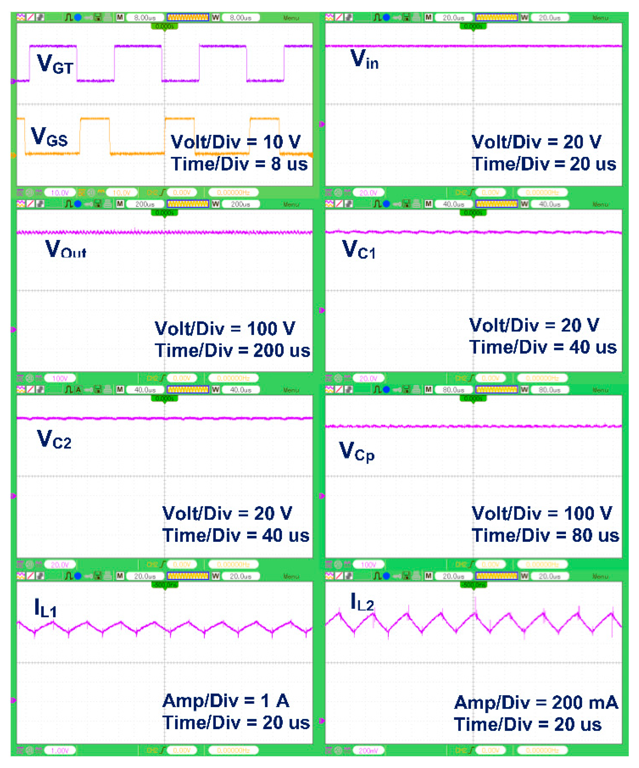
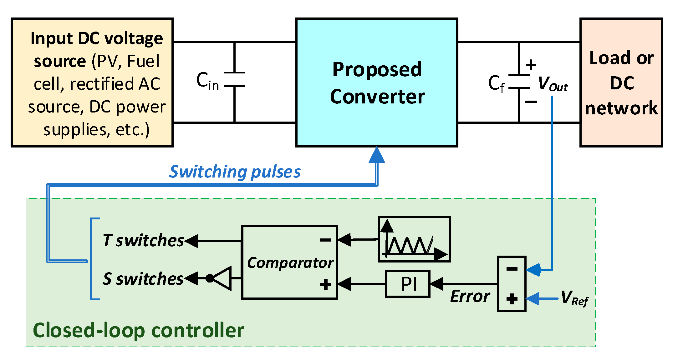
2. Proposed SC Converter Topology

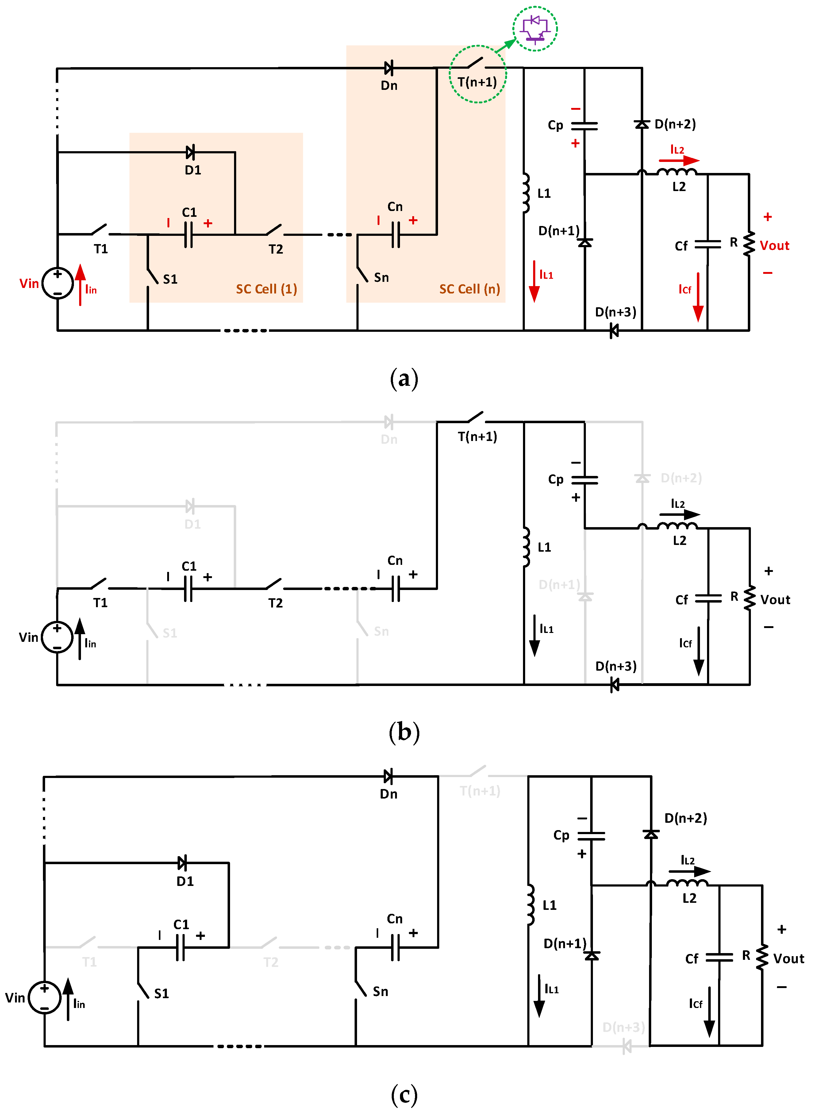
Here, the proposed converter and its operating principles are presented and discussed. 
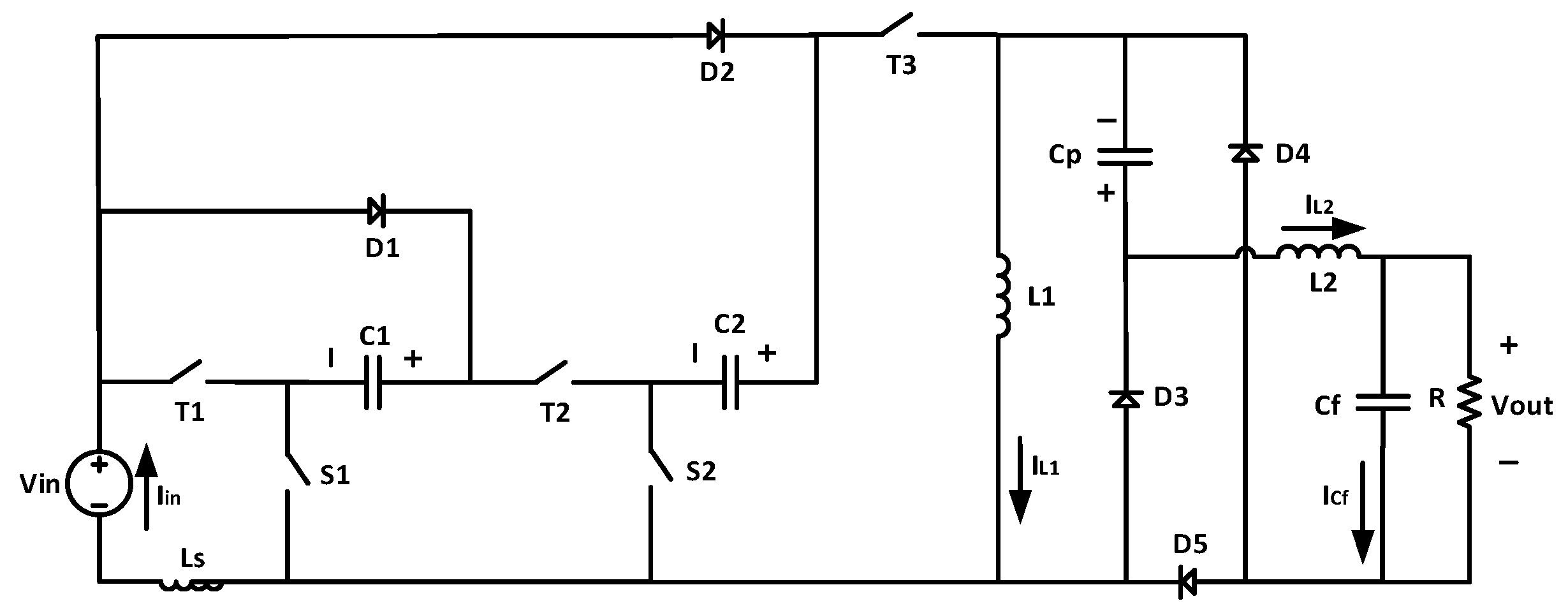
Figure 1a shows the circuit diagram of the proposed converter, consisting of one DC voltage source (Vin), one filtering capacitors Cf, one coupling capacitors Cp, n SCs (C1,…, Cn), two inductors (L1 and L2), one resistive load (R), (2n+1) power switches (T1,…, Tn+1 and S1,…, Sn) and (n+3) diodes (D1, …, Dn+3). As can be seen, the SC cells of the converter include three switching devices. Since the diodes are generally smaller, easier-to-control and cheaper than the switches, a simple combination of switches and diodes is used in the SC cells. As presented in Figure 1b,c, this converter has two operational modes. In Table 1, the operational characteristics of the proposed converter are listed. Generally, in mode 1, by turning on the T switches and Dn+3, the capacitors and the inductors are respectively discharged and charged. In mode 2, the inductors L1 and L2 are discharged to charge the capacitors Cp and Cf, respectively; here, the S switches are conducted, resulting in charging SCs.
In the following, the proposed converter is analyzed in detail. Based on Figure 1, the below statements can be, respectively, expressed for the voltages of inductors L1 and L2:
V L 1 ( t ) = { ( n + 1 ) V i n t ( 0 , D T ] V C p   t [ D T , T )
V L 2 ( t ) = { ( n + 1 ) V i n + V C p V o u t t ( 0 , D T ] V C p t [ D T , T )
In (1) and (2), D, VCp, Vout and Vin, respectively, are the duty-cycle, coupling capacitor voltage, and the converter’s voltages at its output and input ports. T = ( 1 / f s ) is the switching pulses’ periodic time where the switching frequency is denoted by fs. Generally, in the ideal state, an inductor’s average voltage is zero in one full-cycle. So, using (2) and (1), the voltage balances on the first and second inductors (L1 and L2), respectively, give:
0 T V L 1 ( t ) d t = 0 D T V L 1 ( t ) d t + D T T V L 1 ( t ) d t = D ( n + 1 ) V i n ( 1 D ) V C p = 0
0 T V L 2 ( t ) d t = 0 D T V L 2 ( t ) d t + D T T V L 2 ( t ) d t = D [ ( n + 1 ) V i n + V C p V o u t ]   + ( 1 D ) [ V C p V o u t ] = 0
By solving (3), the voltage of the coupling capacitor (Cp) is acquired, as shown below:
V C p = ( n + 1 ) D 1 D V i n
By using (5) in (4), the voltage gain is attained as follows:
G = V o u t V i n = ( n + 1 ) D ( 2 D ) 1 D f o r 0 < D < 1
At this stage, the calculations related to the sizing of the passive components of this converter are presented. Respectively, the currents of the first and second inductors can be expressed as follows:
i L 1 ( t ) = 1 L 1 0 t V L 1 ( t ) d t + i L 1 ( 0 )
i L 2 ( t ) = 1 L 2 0 t V L 2 ( t ) d t + i L 2 ( 0 )
By using (1) and (2) in (7) and (8), the current ripples of the inductors L1 and L2 for t = DT can be respectively obtained as:
Δ i L 1 = 1 L 1 0 D T ( n + 1 ) V i n d t
Δ i L 2 = 1 L 2 0 D T ( ( n + 1 ) V i n + V C p V o u t ) d t
By solving the above equations, the sizes of the first and second inductors are calculated as:
L 1 = D ( n + 1 ) f s Δ i L 1 V i n
L 2 = ( n + 1 ) D ( 1 D ) f s Δ i L 2 V i n
Note that in the proposed structure, SCs have similar voltages (VC1 = VC2 = VC3 =…= VCn) since their sizes and charging currents are similar. Regarding the fact that in the discharging mode, the average values of the SCs’ currents are similar and equal to ( I i n = G I o ) , where Io is the output current of the converter, their voltage ripples for t = TD are expressed as:
Δ V C i = 1 C i 0 D T ( I i n ) d t = 1 C i 0 D T ( G I o ) d t f o r i = 1 , , n
By considering that I o is equal to ( V o u t / R ) and solving (13), the sizing of the SCs can be performed based on (14).
C i = ( n + 1 ) ( 2 D ) D 2 ( 1 D ) Δ V C i f s R V o u t f o r i = 1 , 2 , , n
In the discharging mode, the average current of the coupling capacitor (Cp) is equal to ( I o ) . Consequently, its voltage ripples for t = TD can be expressed as:
Δ V C p = 1 C p 0 D T ( I o ) d t = D T I o C p = D f s C p I o
Thus, the size of this capacitor can be obtained as follows:
C P = D Δ V C p f s R V o u t
In this structure, with an average current of Δ i L 2 / 4 , the output capacitor is charged for T / 2 . Hence, by performing the same procedure, the size of this capacitor is obtained as follows:
C f = Δ i L 2 8 Δ V C f f s = ( n + 1 ) D ( 1 D ) 8 Δ V C f f s 2 L 2 V i n
in which Δ V C f is the voltage ripple of the filtering capacitor. At this step, to obtain the converter efficiency, all components’ power losses are calculated based on the following procedures.
The power loss of switches and diodes includes conduction and switching losses ( P l o s s = P l o s s ( c ) + P l o s s ( s w ) ) which can be computed, respectively, as given below [25,26,27]:
Conduction loss:
P l o s s ( c ) = r o n I r m s 2 + V f I a v e
Switching loss:
P l o s s ( s w ) = ( E o n + E o f f ) f s
In (18) and (19), ron, Irms, Vf, Iave, respectively, are the switch or diode’s internal resistance, current root mean square (RMS) value, on-state voltage, and current average value. In addition, Eoff and Eon, respectively, denote the device’s switching energy losses while turning it off and on.
Power losses of capacitors and inductors consist of conduction losses as follows:
P l o s s = r e s r I r m s 2
in which resr denotes the series equivalent resistance of the device.
Table 2 gives the power losses of all the components, along with their current and voltage equations. In consequence, the total power loss (PTotalLoss) can be gained by summing up the power losses of all components. Therefore, the efficiency of this converter is calculated as:
% η = P o u t P o u t + P T o t a l L o s s × 100
In (21), Pout denotes the converter output power.

3. Comparisons

Here, different converters in the same class, including the proposed topology, are thoroughly compared in terms of the voltage gain, voltage stress on the switching devices and SCs, number of components, efficiency, and so forth. In Table 3, the main specifications of the step-up and/or step-down converters with expansion ability, including the proposed converter, are listed.
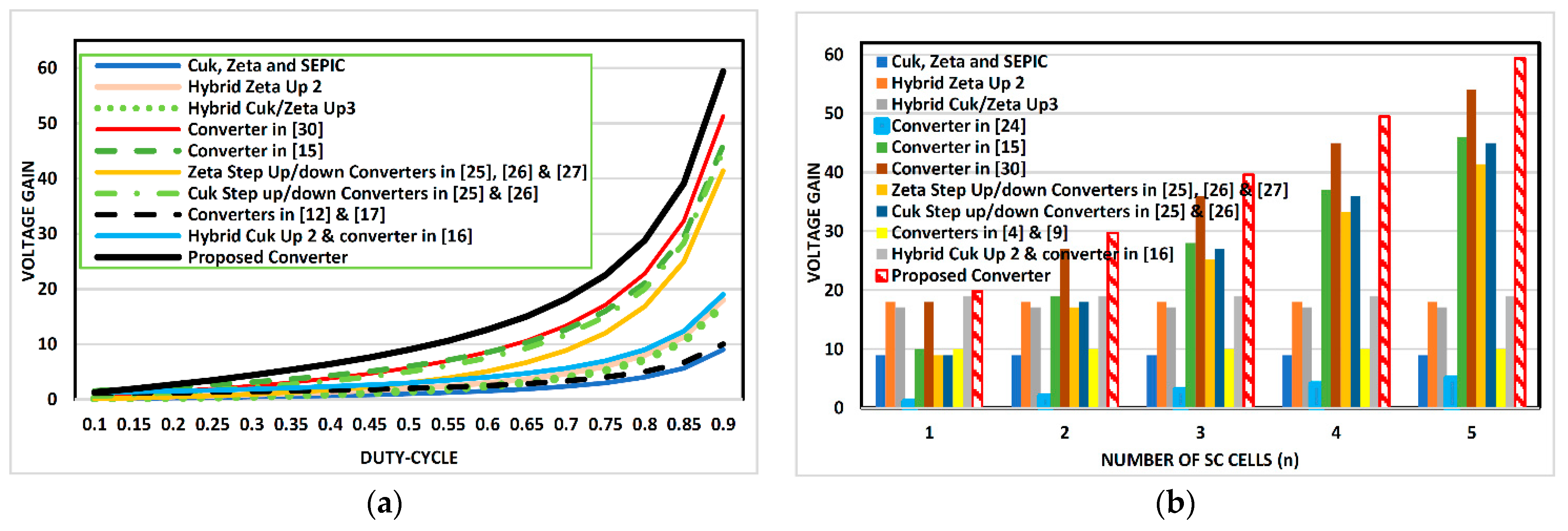
In Figure 2a, the voltage gains of various structures are compared by considering n = 5 and 0.1 ≤ D ≤ 0.9. This comparison contains both expandable and non-expandable converters. As seen, the highest voltage gain is provided by the proposed converter for all duty-cycles (0.1–0.9). In other words, the proposed converter is the best choice for modern applications requiring a high gain of voltage. It is worth noting that the converters presented in [24,28,29] can provide a fixed voltage gain while the proposed topology can produce a variable voltage gain making it suitable for applications, such as RESs, that require continuous voltage regulation at their output port. In addition, Figure 2b shows the voltage gains of different converters by considering D = 0.9 and n = 1, 2, 3, 4, 5. As seen, the proposed converter is able to produce a higher voltage gain even by using a lower number of SC modules/cells. For instance, the proposed converter with n = 4 generates a voltage gain of 49.5 which is higher than the voltage gains provided by the others with more SC cells (n = 5).
By considering the points mentioned above and using Table 3, the numbers of all components in the proposed structure for n = 4 and the other converters for n = 5 are calculated and given in Table 4. As can be seen, the proposed converter employs the fewest passive components, i.e., two inductors and six capacitors. Among the converters, the converter of [15] has the largest number of passive components, i.e., 13 capacitors and 6 inductors, and the highest total number of components, i.e., 28 components, imposing heavy penalties on cost, size, and efficiency of this converter.
Regarding the total number of components, Table 4 clearly shows that the proposed topology has the third place, since it employs 24 components. The converter of [27] and the Zeta and Cuk converters of [25,26] have the lowest total number of components, i.e., 22 components. Additionally, the second place belongs to the Zeta and Cuk converters of [26] with 23 components. However, it is noteworthy that only by using one/two more components, the proposed structure provides a voltage gain that is 10–20% higher than the voltage gains of these five converters. For instance, the proposed converter with n = 4 provides the voltage conversion ratio of 49.5, while the Zeta converters of [25,27] with n = 5 generate the voltage gain of 41.5. Generally, the more the SC modules’ number augments, the more this gap increases. This implies that for applications that require high voltage conversion ratio, the proposed SC structure is the best choice. Note that compared to the rest of the converters, the proposed SC converter uses fewer or equal number of power components.
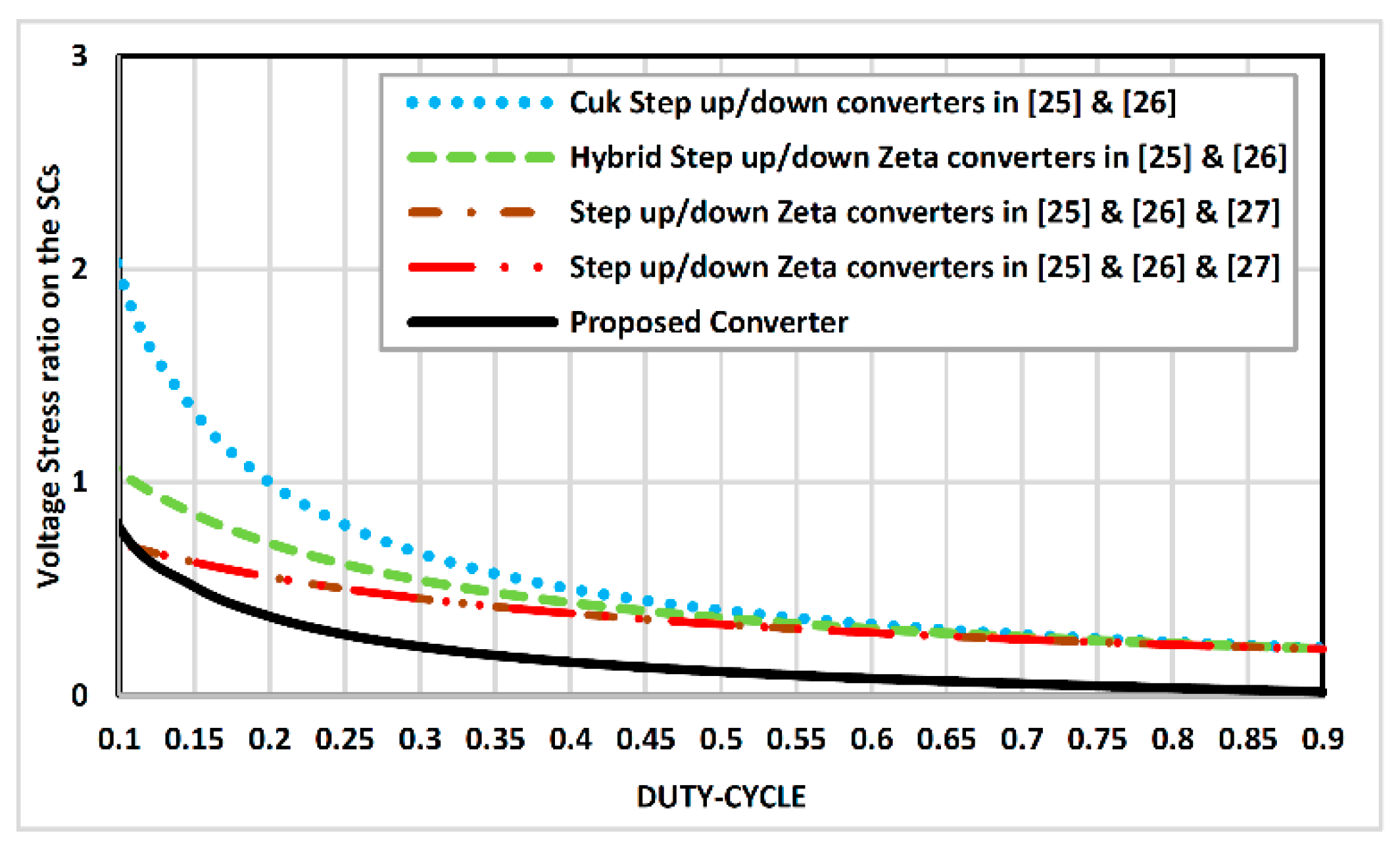
In the following, the comparison results for diverse expandable converters in the same class in terms of maximum voltage stresses on their components such as their switching devices and SCs are presented. Accordingly, based on [27], the parameter VR (ratio of the maximum voltage stress on the power device to the output voltage) is defined as follows:
V R = V max V o u t
where Vmax denotes the maximum voltage stress on the power component (i.e., switch or SCs) and Vout represents the converter voltage at its output port.
Figure 3 presents the values of VR obtained for SCs of different expandable converters by considering n = 5. According to this figure, the proposed converter imposes the less voltage stress on the SCs. 
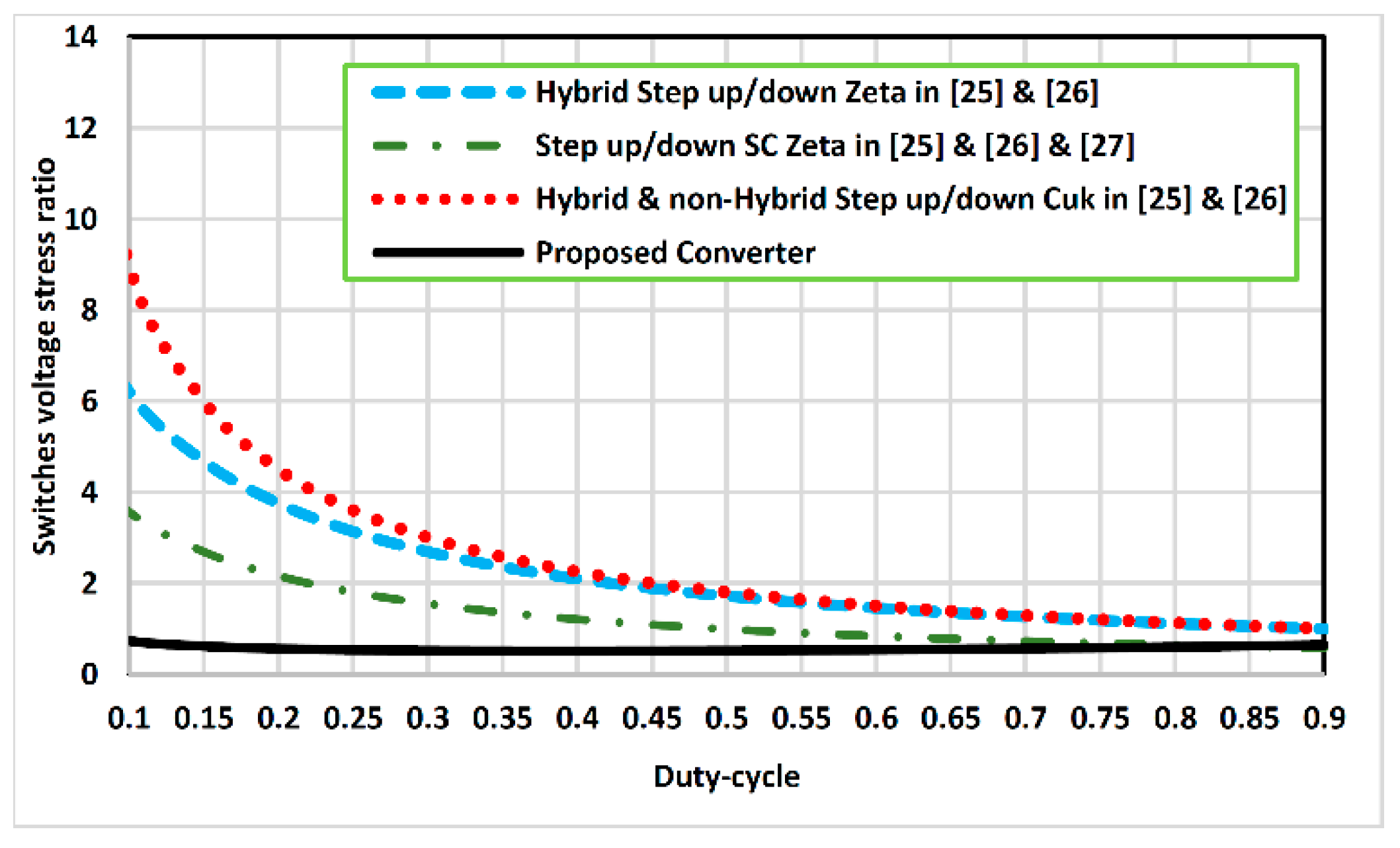
Figure 4 presents the curve of VR obtained for comparing the voltage stress on the switches of different converters by considering n = 5. As seen, for D < 0.75, the least voltage stress on the switches belongs to the proposed structure. In addition, for the rest of duty-cycles, our converter presents a very close performance to step-up/down Zeta converters of [25,26,27] which have the best performances.
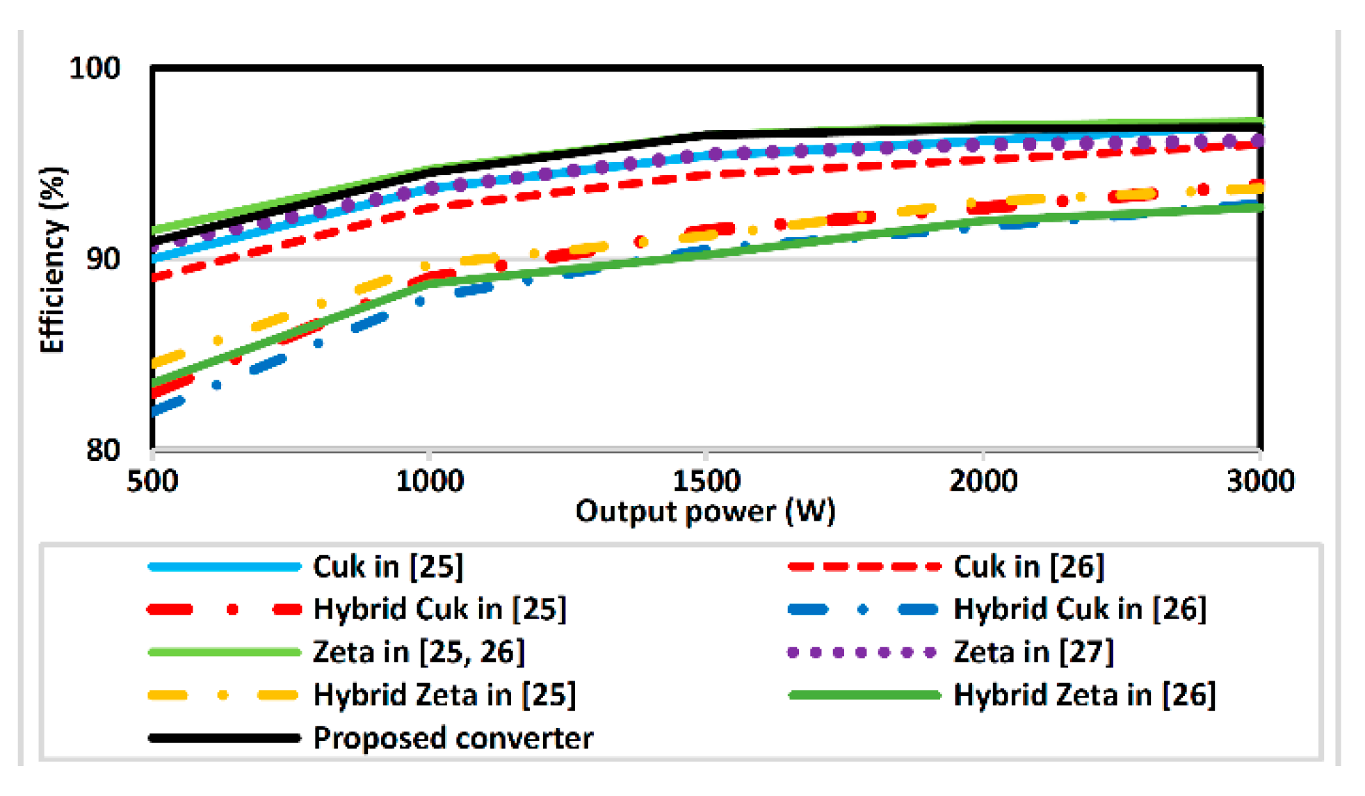
Figure 5 presents the efficiency curve of different modular/extendible SC hybrid and non-hybrid converters, including the proposed one in terms of output power. Since the proposed topology can provide a higher voltage gain with fewer SC cells/modules compared to the others, the parameter n is considered as 1 and 2 for the proposed converter and the others, respectively. As clearly seen, the proposed converter provides a very desirable efficiency compared to the other topologies in the same class. It should be noted that, even in comparison to the traditional non-expandable converters like Zeta, Cuk, Sepic, hybrid converters of [11], and so forth, the proposed converter is a better option for applications with very high voltage gains. For providing such a voltage gain with a non-extreme duty-cycle, the conventional converters should be employed in cascaded structures, which immensely reduces the total efficiency [25,26,27].
Based on the already-given comparisons, the best converter structures are listed for different factors in Table 5. As seen, the proposed extendible converter is among the best structures or is the best one for all comparisons. As seen, the proposed converter employs the least number of passive components. It can provide higher voltage conversion ratios in lower duty-cycles. Thus, it is not necessary to use a high-speed and -cost control system. The proposed topology imposes less voltage stress on its power components, such as the power switches and the SCs. Additionally, this converter also has desirable performance in terms of efficiency. In conclusion, the proposed SC structure possesses clear and robust superiorities over other ones, especially in applications requiring high voltage conversion ratios.
As the last part of this section, the reliability of the proposed expandable converter is briefly discussed. To this end, initially, the proposed converter is compared with the non-expandable converters and then with the expandable ones. Over the non-expandable converters (conventional ones), the prominent advantage of expandable converters, such as the proposed one is their capability of providing higher voltage gains in lower duty-cycles. By avoiding extreme duty-cycles, the reliability of the system will be increased since using such duty-cycles may cause serious problems, such as malfunctions in high switching frequencies. To achieve high voltage gains using non-extreme duty-cycles, the non-expandable converters must be cascaded or use transformer which both are not desirable due to reduced reliability, decreased efficiency and increased cost and size. Thus, compared to non-expandable converters, the proposed converter provides higher reliability for applications needing high voltage gains. Moreover, based on the presented comparisons summarized in Table 5, the proposed one has better performance in comparison to other expandable converters. This converter can provide higher voltage gains using fewer or close number of components compared to the others. In addition, in terms of voltage stress imposed on the components, the proposed one is the superior one. This means that this converter possesses a higher or close reliability compared to others.
It is noteworthy that being a modular and expandable converter does not mean that the proposed converter always needs to employ a large number of components and SC modules. To be more specific, this issue depends on the application and its requirements. According to these conditions, the designer will design the converter in the best possible way. As discussed in the previous comparisons presented for some predefined and certain conditions, the proposed converter can show better performance by having higher voltage gain, less voltage stress on components and fewer or close number of components. For instance, based on Figure 2b and Table 4, it is shown that, over other structures, the proposed converter is able to generate higher voltage gain with lower duty-cycles while employing fewer or close number of components. This means that the proposed converter has better reliability and efficiency compared to other structures for a given condition, which should be considered in the design.

4. Experimental Results

In this section, the performance of our topology is proved in two steps based on experimental results in which the number of SC modules/cells (n) and the frequency of switching (fs) are considered to be 2 and 25 kHz, respectively. In addition, the maximum ripple of inductor currents and capacitor voltages are assumed to be 35% and 10%. In Figure 6, the experimental setup of the proposed converter is shown in which ultra-fast diodes (UG12), TLP250 drivers, and MOSFETs (47N60C) are used. In addition, Figure 7 shows the proposed converter when n = 2. Here, the converter parameters are calculated. It is noteworthy that the switches will need to be synchronized, especially when n is large. However, switching synchronization will not be a challenging issue with the current technologies since even by using a conventional microcontroller, this aim can be achieved [16].

4.1. First Step: Experimental Results with Non-feedback Controller for Different Operating Conditions

At the first step, the proposed structure’s performance with a non-feedback control system is validated for two different conditions as listed below:
  • The output and input voltages are 180 V and 40 V.
  • The output and input voltages are 508 V and 80 V.
For obtaining 180 V at the output with the input voltage of 40 V, the voltage gain provided by the converter should be equal to 4.5. According to (6), the duty-cycle is gained as D = 50%. Based on (11) and (12), L2 and L1 have to be sized as greater than 3 mH and 1.4 mH, respectively. Thus, their sizes are considered to be L1 = 1.5 mH and L2 = 3 mH. Based on (14), (16), and (17), SCs, coupling capacitor, and filtering capacitor have to be more than 8.44 μ F , 1.9 μ F and 110 n F . The parameters and specifications used for the experimental set of our converter are listed in Table 6. Note that, in all experiments, the inductor LS is a very small inductor employed to confine the current peak.
Figure 8 shows the results of the first experiment of the converter where D is equal to 0.5. As evidently shown, the S and T switches are respectively controlled by using two switching pulses, named VGS and VGT. By having the input voltage (Vin) of 40 V, the proposed converter can provide about 177 V at the output (VO = 177 V), which is desirable. Additionally, a desirable voltage, i.e., 40 V with acceptable voltage ripples, is achieved in both of the SCs (C1 and C2). In addition, the coupling capacitor has a desirable voltage of 118.5 V. Moreover, as seen, the currents of the inductors, denoted by IL1 and IL2, are presented, which are plausible since they are in continuous current mode with acceptable average values. The input current is shown, which is continuous as claimed. Moreover, this figure presents the voltages of the switching devices. As shown, the voltages of the power switches T1 and T3, denoted by VT1 and VT3, are similar, and their maximum value is about 42 V. In addition, the voltage stress on the switch S2 (VS2 = 83 V) is around two times as that of the power switch S1 (VS1 = 41 V). Moreover, the switch T2 also has a desirable voltage (VT2 = 167 V). All switches follow the defined switching pattern correctly.
By considering 80 V and 508 V as the input and output voltages in the second experiment, the voltage gain is calculated as 6.35, which in turn gives the duty-cycle of 60% based on (6). The sizes of the inductors L1 and L2 must, respectively, be more than 2.5 mH and 6.5 mH according to (11) and (12). Hence, their sizes are considered to be L1 = 3 mH and L2 = 6.5 mH. Based on (14) and (16)–(17), the sizes of the SCs, coupling capacitor, and filtering capacitor must be selected more than 6.3 μ F , 672 n F and 35 n F . The parameters utilized for the second experimental set of the converter are listed in Table 7.
In Figure 9, the second experiment’s results are shown in which the switching pulses VGT and VGS are presented. As seen, the input DC voltage is equal to 80 V. In addition, the output voltage is favorable (VO = 505 V). As seen, all of the capacitors C2, C1, and Cp are respectively charged to 79.8 V, 79.7 V, and 357 V, which are entirely acceptable. In this figure, the continuous current waveforms of the first and second inductors of the proposed converter are also shown, and their mean values are obtained as IL1 = 3.75 A and IL2 = 1 A. Thus, their currents are continuous waveforms with acceptable mean values and ripples.

4.2. Second Step: Experimental Results with Open- and Closed-Loop Controllers in the Presence of a Step Change in the Input Voltage

In this section, the performance of the SC converter with closed- and open-loop control systems is investigated by step changing the value of the input DC voltage from 68 V to 50 V. As seen in Figure 10, presenting the general test system, a simple feed-back control system is used here. This system can provide a constant voltage at the output port of the converter under input voltage changes. In this system, the average value of the output voltage of the SC converter is continuously measured and compared with the reference value leading to generating the switching pulses for the converter. In this section, the load is considered equal to 184.5 Ω and the rest of the parameters are as those listed in Table 7.
In Figure 11, the converter’s experimental results with and without the feedback control system are shown in the existence of a step-change in the input voltage. Figure 11a presents the results with an open-loop control system. As seen, without having a feed-back system, the output voltage of the converter is suddenly changed from 305 V to 225 V by decreasing the input voltage from 68 V to 50 V. In addition, the voltages across the capacitors C1 and Cp are changed from 68 V to 50 V and from 202 V to 148 V, respectively, by applying the step change. It is clearly seen that the converter’s performance with an open-loop control system is acceptable since its stability is maintained.
Figure 11b shows the experimental results of the converter when the closed-loop control system is employed. As seen, in spite of applying the step change in the input voltage (from 68 V to 50 V), the converter can provide the intended output voltage (305 V). As shown, the voltages of the capacitors C1 and Cp are, respectively, changed from 68 V to 50 V and from 202 V to 221 V, which are completely favorable. In other words, the proposed converter with the presented closed-loop control system is able to maintain its stability and provide the reference voltage at its output successfully. Hence, the dynamic performance of this DC–DC topology is validated completely.
In summary, the experimental results of this converter topology are in great agreement with the analysis, proving its desirable performance.

5. Conclusions

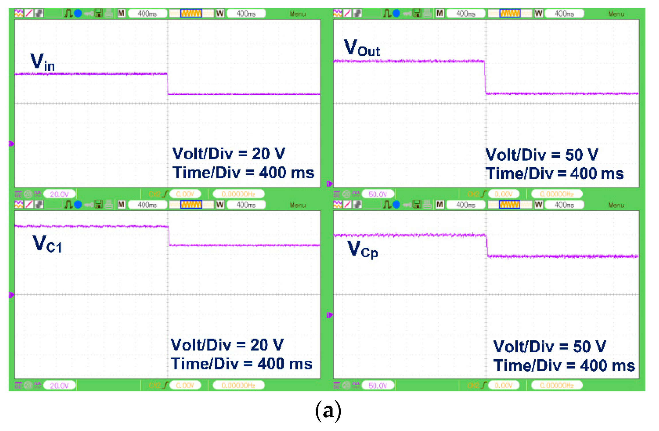
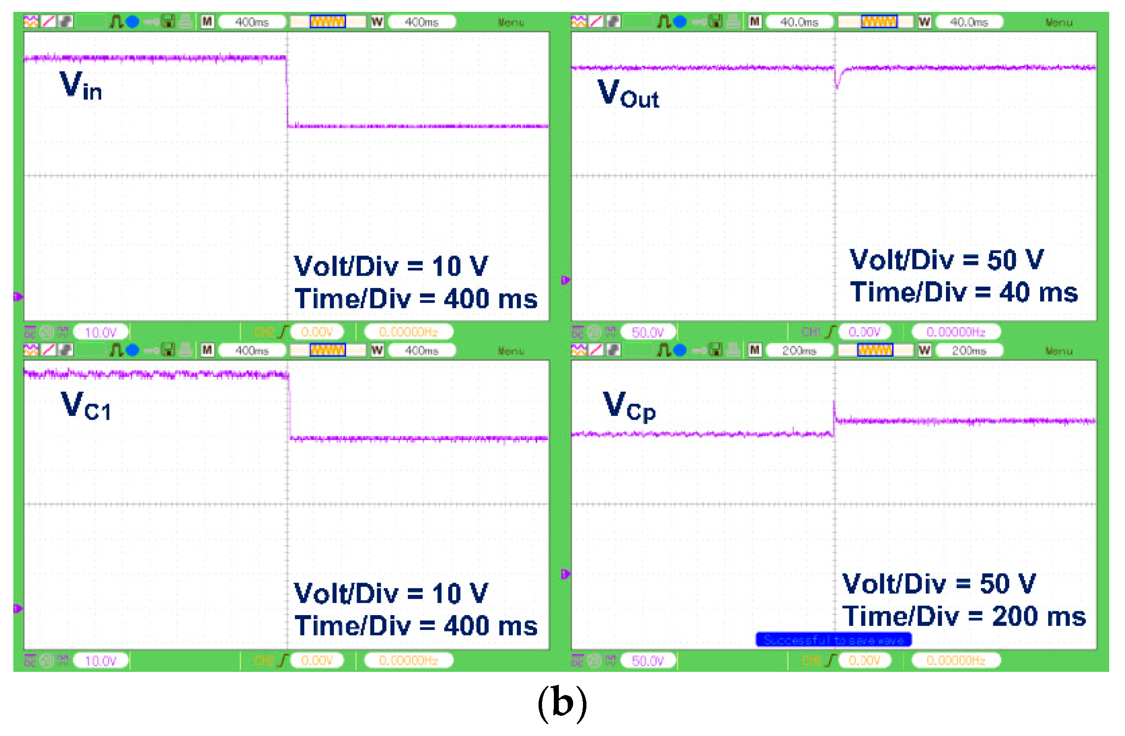
For contemporary applications, such as RESs, ESSs and HVDC systems, this article offers a new step-up/down DC–DC converter with several advantages such as increased voltage conversion ratio and reduced voltage stress on SC capacitors and power switches in comparison with other converter structures. As demonstrated by the comparison and experimental results, higher voltage gains can be provided by this converter, even by using non-extreme duty-cycles. Moreover, due to its guaranteed continuous input current, the extraction of the maximum power from RESs, such as solar panels, is possible using this converter. Based on the results, the proposed SC topology shows a desirable performance and is appropriate for industrial applications demanding high voltage gains. It is worthy of mentioning that in the applications needing high voltage conversion ratios along with both step-up and -down features, the proposed converter can be employed. For instance, it can be used in HVDC systems to provide the desired voltage level and fast regulation. As already stated, to avoid high values of duty-cycles and high voltage stresses on different components in the converter circuit, several conventional topologies must be cascaded with each other to achieve high voltage conversion ratios, which can cause serious drawbacks like decreased efficiency and increased total number of components. Consequently, the proposed converter is a better option for such applications because of its modular structure.
In future works, the most effective soft-switching methods for the expandable SC-based step-up/down converters, including the proposed converter, will be studied which in turn may result in advantages like increased efficiency, decreased power losses, increased life-spans for the employed components, and so forth.

Author Contributions

Conceptualization, M.A. and E.A.; data curation, M.A. and E.A.; formal analysis, M.A. and E.A.; investigation, E.A., L.L. and B.T.; methodology, M.A.; software, E.A. and B.T.; supervision, L.L.; validation, M.A., E.A., L.L. and B.T.; visualization, M.A. and E.A.; Writing—original draft, M.A. and E.A.; Writing—review and editing, M.A., E.A., L.L. and B.T. All authors have read and agreed to the published version of the manuscript.

Funding

This research received no external funding.

Institutional Review Board Statement

Not applicable.

Informed Consent Statement

Not applicable.

Data Availability Statement

Not applicable.

Conflicts of Interest

The authors declare no conflict of interest.

References

  1. Uddin, M.; Biswas, S.P.; Islam, M.; Anower, M.; Kouzani, A.Z.; Mahmud, M.A. A new generalized step-down single-stage AC/AC power converter. Sustainability 2020, 12, 9181. [Google Scholar] [CrossRef]
  2. Gaisse, P.; Muñoz, J.; Villalón, A.; Aliaga, R. Improved predictive control for an asymmetric multilevel converter for photovoltaic energy. Sustainability 2020, 12, 6204. [Google Scholar] [CrossRef]
  3. Korth Pereira Ferraz, P.; Kowal, J. A Comparative study on the influence of DC/DC-converter induced high frequency current ripple on lithium-ion batteries. Sustainability 2019, 11, 6050. [Google Scholar] [CrossRef] [Green Version]
  4. Alsokhiry, F.; Adam, G. Multi-port DC-DC and DC-AC converters for large-scale integration of renewable power generation. Sustainability 2020, 12, 8440. [Google Scholar] [CrossRef]
  5. Rajaei, A.; Shahparasti, M.; Nabinejad, A.; Savaghebi, M. A high step-up partial power processing DC/DC T-source converter for UPS application. Sustainability 2020, 12, 10464. [Google Scholar] [CrossRef]
  6. Song, S.; Hu, Y.; Ni, K.; Yan, J.; Chen, G.; Wen, H.; Ye, X. Multi-port high voltage gain modular power converter for offshore wind farms. Sustainability 2018, 10, 2176. [Google Scholar] [CrossRef] [Green Version]
  7. Shalchi, A.; Abbasi, M.; Abbasi, E.; Tousi, B.; Gharehpetian, G.B. New DTR line selection method in a power system comprising DTR, ESS, and RES for increasing RES integration and minimising load shedding. IET Gener. Transm. Distrib. 2020, 14, 6319–6329. [Google Scholar] [CrossRef]
  8. Abbasi, M.; Miyab, M.S.; Tousi, B.; Gharehpetian, G.B. Using dynamic thermal rating and energy storage systems technologies simultaneously for optimal integration and utilization of renewable energy sources. Int. J. Eng. 2020, 33, 92–104. [Google Scholar]
  9. Rezvanyvardom, M.; Mirzaei, A. High gain configuration of modified ZVT SEPIC-Boost DC-DC converter with coupled inductors for photovoltaic applications. Sol. Energy 2020, 208, 357–367. [Google Scholar] [CrossRef]
  10. Siwakoti, Y.P.; Mostaan, A.; Abdelhakim, A.; Davari, P.; Soltani, M.N.; Khan, M.N.H.; Li, L.; Blaabjerg, F. High-voltage gain quasi-SEPIC DC–DC converter. IEEE J. Emerg. Sel. Top. Power Electron. 2019, 7, 1243–1257. [Google Scholar] [CrossRef] [Green Version]
  11. Axelrod, B.; Berkovich, Y.; Ioinovici, A. Switched-capacitor/switched-inductor structures for getting transformerless hybrid DC–DC PWM converters. IEEE Trans. Circuits Syst. I Regul. Pap. 2008, 55, 687–696. [Google Scholar] [CrossRef]
  12. Muranda, C.; Ozsoy, E.; Padmanaban, S.; Bhaskar, M.S.; Fedak, V.; Ramachandaramurthy, V.K. Modified SEPIC DC-to-DC boost converter with high output-gain configuration for renewable applications. In Proceedings of the 2017 IEEE Conference on Energy Conversion (CENCON), Kuala Lumpur, Malaysia, 30–31 October 2017. [Google Scholar]
  13. Banaei, M.R.; Bonab, H.A.F. A Novel Structure for Single-Switch Nonisolated Transformerless Buck–Boost DC–DC Converter. IEEE Trans. Ind. Electron. 2017, 64, 198–205. [Google Scholar] [CrossRef]
  14. Kishore, G.I.; Tripathi, R.K. Single-phase PFC converter using switched capacitor for high voltage DC applications. IEEE Trans. Ind. Appl. 2018, 54, 2560–2567. [Google Scholar] [CrossRef]
  15. Kishore, G.I.; Tripathi, R.K. A novel high voltage gain single-phase AC-DC PFC converter using switched-capacitor. In Proceedings of the 2017 4th International Conference on Power, Control & Embedded Systems (ICPCES), Allahabad, India, 9–11 March 2017. [Google Scholar]
  16. Saravanan, S.; Babu, N.R. A modified high step-up non-isolated DC-DC converter for PV application. J. Appl. Res. Technol. 2017, 15, 242–249. [Google Scholar] [CrossRef]
  17. Oluwafemi, A.W.; Ozsoy, E.; Padmanaban, S.; Bhaskar, M.S.; Ramachandaramurthy, V.K.; Fedak, V. A modified high output-gain cuk converter circuit configuration for renewable applications—A comprehensive investigation. In Proceedings of the 2017 IEEE Conference on Energy Conversion (CENCON), Kuala Lumpur, Malaysia, 30–31 October 2017. [Google Scholar]
  18. Kishore, G.I.; Tripathi, R.K. Single-phase PFC converter using modified multiplier SEPIC converter for high voltage DC applications. In Proceedings of the Fourth IEEE Uttar Pradesh Section International Conference on Electrical, Computer and Electronics, Mathura, India, 26–28 October 2017. [Google Scholar]
  19. Maalandish, M.; Hosseini, S.H.; Jalilzadeh, T. High step-up DC/DC converter using switch-capacitor techniques and lower losses for renewable energy applications. IET Power Electron. 2018, 11, 1718–1729. [Google Scholar] [CrossRef]
  20. Ye, Y.; Peng, W.; Jiang, B. High step-up DC–DC converter with multi-winding CL and switched capacitor. IET Power Electron. 2018, 11, 2232–2240. [Google Scholar] [CrossRef]
  21. Babaei, E.; Saadatizadeh, Z.; Cecati, C. High step-up high step-down bidirectional DC/DC converter. IET Power Electron. 2017, 10, 1556–1571. [Google Scholar] [CrossRef]
  22. Cao, D.; Peng, F.Z. A family of zero current switching switched-capacitor dc-dc converters. In Proceedings of the 2010 Twenty-Fifth Annual IEEE Applied Power Electronics Conference and Exposition (APEC), Palm Springs, CA, USA, 21–25 February 2010. [Google Scholar]
  23. Choi, H.; Jang, M.; Pou, J. High-gain soft-switching interleaved switched-capacitor DC–DC converter with phase-shedding technique. IET Power Electron. 2017, 10, 1013–1022. [Google Scholar] [CrossRef]
  24. Abbasi, M.; Abbasi, E.; Tousi, B.; Gharehpetian, G.B. A zero-current switching switched-capacitor DC-DC converter with reduction in cost, complexity, and size. Int. J. Circuit Theory Appl. 2019, 47, 1630–1644. [Google Scholar] [CrossRef]
  25. Abbasi, M.; Babaei, E.; Tousi, B. New family of non-isolated step-up/down and step-up switched-capacitor-based DC–DC converters. IET Power Electron. 2019, 12, 1706–1720. [Google Scholar] [CrossRef]
  26. Abbasi, M.; Abbasi, E.; Tousi, B.; Gharehpetian, G.B. New family of expandable step-up/-down DC-DC converters with increased voltage gain and decreased voltage stress on capacitors. Int. Trans. Electr. Energy Syst. 2020, 30, e12252. [Google Scholar] [CrossRef]
  27. Vosoughi, N.; Abbasi, M.; Abbasi, E.; Sabahi, M. A Zeta-based switched-capacitor DC-DC converter topology. Int. J. Circuit Theory Appl. 2019, 47, 1302–1322. [Google Scholar] [CrossRef]
  28. Qian, W.; Cao, D.; Cintron-Rivera, J.G.; Gebben, M.; Wey, D.; Peng, F.Z. A switched-capacitor DC–DC converter with high voltage gain and reduced component rating and count. IEEE Trans. Ind. Appl. 2012, 48, 1397–1406. [Google Scholar] [CrossRef]
  29. Shen, M.; Peng, F.Z.; Tolbert, L.M. Multilevel DC–DC power conversion system with multiple DC sources. IEEE Trans. Power Electron. 2008, 23, 420–426. [Google Scholar] [CrossRef]
  30. Vosoughi Kurdkandi, N.; Farhadi, M.; Babaei, E.; Ghavidel, P. Design and analysis of a switched-capacitor DC-DC converter with variable conversion ratio. Int. J. Circuit Theory Appl. 2020, 48, 1638–1657. [Google Scholar] [CrossRef]
  31. Abbasi, M.; Abbasi, E.; Li, L. New transformer-less DC–DC converter topologies with reduced voltage stress on capacitors and increased voltage conversion ratio. IET Power Electron. 2021, 14, 1173–1192. [Google Scholar] [CrossRef]
  32. Abbasi, M.; Nazari, Y.; Abbasi, E.; Li, L. A new transformer-less step-up DC–DC converter with high voltage gain and reduced voltage stress on switched-capacitors and power switches for renewable energy source applications. IET Power Electron. 2021. [Google Scholar] [CrossRef]
  33. Eshkevari, A.L.; Mosallanejad, A.; Sepasian, M. A new step-up Dc/Dc converter based on lcct Z-source and switched-capacitor cell. In Proceedings of the 2020 11th Power Electronics, Drive Systems, and Technologies Conference (PEDSTC), Tehran, Iran, 4–6 February 2020; pp. 1–6. [Google Scholar]
  34. Ahmad, A.; Shiluveru, K.; Singh, R.K. Switched capacitor-based continuous input current high step-up impedance source DC–DC converter. IET Power Electron. 2020, 13, 4204–4213. [Google Scholar] [CrossRef]
  35. Sedaghati, F.; Pourjafar, S. Analysis and implementation of a boost DC–DC converter with high voltage gain and continuous input current. IET Power Electron. 2019, 13, 798–807. [Google Scholar] [CrossRef]
Figure 1. (a) Proposed converter; and its operational (b) mode 1 (c) mode 2.
Sustainability 13 05243 g001
Figure 2. Voltage gain comparison of different converters for (a) different duty-cycles and n = 5 and (b) a different number of SCs and D = 0.9.
Sustainability 13 05243 g002
Figure 3. Comparison of voltage stress on the SCs of different topologies (n = 5).
Sustainability 13 05243 g003
Figure 4. Comparison of voltage stress on the power switches of different converters (n = 5).
Sustainability 13 05243 g004
Figure 5. Efficiencies of different converters in terms of output power.
Sustainability 13 05243 g005
Figure 6. The proposed SC converter’s experimental circuits.
Sustainability 13 05243 g006
Figure 7. Proposed converter when n = 2.
Sustainability 13 05243 g007
Figure 8. Experimental results of the proposed converter for D = 0.5.
Sustainability 13 05243 g008
Figure 9. Experimental results of the proposed converter for D = 0.6.
Sustainability 13 05243 g009
Figure 10. Simple block diagram of the test system including the proposed converter with a closed-loop controller for output voltage regulation.
Sustainability 13 05243 g010
Figure 11. Experimental results of the proposed converter with step change in input voltage using an (a) open-loop and (b) closed-loop control system.
Sustainability 13 05243 g011aSustainability 13 05243 g011b
Table 1. Operational characteristics of the converter.
Operation ModeSwitching StatesCharging (+)/Discharging (−) States
T1,…,Tn+1S1,…,SnD1,…,Dn+2Dn+3C1,…,CnCpL1L2
11001++
20110++
Table 2. Voltage, current and power loss of the components in the proposed converter.
Comp.VoltageCurrentSwitching LossConduction Loss
T1,, Tn { 0 t ( 0 , D T ] V i n t [ D T , T ) { I i n t ( 0 , D T ] 0 t [ D T , T ) n [ V i n I i n f s 6 ( t o n + t o f f ) ] r o n ( s ) D I i n 2 + V f ( s ) D I i n
Tn+1 { 0 t ( 0 , D T ] ( 1 + n D 1 D ) V i n t [ D T , T ) { I i n t ( 0 , D T ] 0 t [ D T , T ) V i n I i n f s 6 ( 1 + n D 1 D ) ( t o n + t o f f ) r o n ( s ) D I i n 2 + V f ( s ) D I i n
S1,, Sn { m V i n t ( 0 , D T ] f o r m = 1 , , n 0 t [ D T , T ) { 0 t ( 0 , D T ] I i n n t [ D T , T ) m = 1 n m V i n I i n f s 6 n ( t o n + t o f f ) m = 1 n ( r o n ( s ) ( 1 D ) I i n 2 n 2 + m V f ( s ) ( 1 D ) I i n n )
D1,, Dn { m V i n t ( 0 , D T ] f o r m = 1 , , n 0 t [ D T , T ) { 0 t ( 0 , D T ] I i n n t [ D T , T ) m = 1 n m V i n I i n f s 6 n ( t o n + t o f f ) r o n ( D ) ( 1 D ) I i n 2 n + V f ( D ) ( 1 D ) I i n
Dn+1 { ( n + 1 1 D ) V i n t ( 0 , D T ] 0 t [ D T , T ) { 0 t ( 0 , D T ] I L 1 t [ D T , T ) ( n + 1 ) V i n I L 1 f s 6 ( 1 D ) ( t o n + t o f f ) r o n ( D ) ( 1 D ) I L 1 2 + V f ( D ) ( 1 D ) I L 1
Dn+2 { ( n + 1 ) V i n t ( 0 , D T ] 0 t [ D T , T ) { 0 t ( 0 , D T ] I o t [ D T , T ) ( n + 1 ) V i n I o f s 6 ( t o n + t o f f ) r o n ( D ) ( 1 D ) I o 2 + V f ( D ) ( 1 D ) I o
Dn+3 { 0 t ( 0 , D T ] D ( n + 1 ) ( 1 D ) t [ D T , T ) { I o t ( 0 , D T ] 0 t [ D T , T ) D ( n + 1 ) V i n I o f s 6 ( 1 D ) ( t o n + t o f f ) r o n ( D ) D I o 2 + V f ( D ) D I o
L1 { ( n + 1 ) V i n t ( 0 , D T ] V C p t [ D T , T ) I i n D = G I o D = ( n + 1 ) ( 2 D ) ( 1 D ) I o r e s r ( L 1 ) ( ( n + 1 ) ( 2 D ) 1 D I o ) 2
L2 { ( n + 1 ) V i n + V C p V o u t t ( 0 , d T ] V C p t [ D T , T ) I o = ( n + 1 ) D ( 2 D ) R ( 1 D ) V i n r e s r ( L 2 ) I o 2
C1,, Cn V i n { I i n t ( 0 , D T ] I i n n t [ D T , T ) n × r e s r ( C i ) I i n 2 ( D + 1 D n 2 ) 2
Cp ( n + 1 ) D 1 D V i n { I o t ( 0 , D T ] I L 1 I o t [ D T , T ) r e s r ( C p ) I o 2
Cf ( n + 1 ) D ( 2 D ) 1 D V i n D ( n + 1 ) 4 f s L 1 V i n r e s r ( C f ) 16 f s 2 ( ( n + 1 ) D ( 1 D ) V i n ) 2
Table 3. Specifications of different expandable switched-capacitor/-inductor DC–DC converter topologies.
StructureVoltage GainMaximum Voltage StressNumber of Components
SCsT SwitchesCap.Induct.PassiveSw.DiodeTotal
Converter in [15] [ 1 + ( n 1 ) D ] ( 1 D ) 2n + 3n + 13n + 41n + 34n + 8
Converter in [24]n V i nn2nn2n − 15n − 1
Zeta Converter [25] [ D + ( n 1 ) D 2 ] ( 1 D ) V i ( D / ( 1 D ) ) V i ( ( n 1 ) D ( 1 D ) ) n + 12n + 32n − 1n4n + 2
Zeta Hybrid in [25] [ D + ( 2 n 1 ) D 2 ] ( 1 D ) V i ( 2 D / ( 1 D ) ) V i ( 2 ( n 1 ) D ( 1 D ) ) n + 13n + 42n − 1n+34n + 6
Cuk Converter in [25] n D / ( 1 D ) V i ( 1 / ( 1 D ) ) V i ( ( n 1 ) D ( 1 D ) ) n + 12n + 32n − 1n4n + 2
Cuk Hybrid [25] n D [ 1 + D ] ( 1 D ) V i ( ( 1 + D ) / ( 1 D ) ) V i ( ( n 1 ) ( 1 + D ) ( 1 D ) ) n + 13n + 42n − 1n+34n + 6
Zeta Converter in [26] [ D + ( n 1 ) D 2 ] ( 1 D ) V i ( D / ( 1 D ) ) V i ( ( n 1 ) D ( 1 D ) ) n + 12n + 3n + 12n-14n + 3
Zeta Hybrid in [26] [ D + ( 2 n 1 ) D 2 ] ( 1 D ) V i ( 2 D / ( 1 D ) ) V i ( 2 ( n 1 ) D ( 1 D ) ) n + 13n + 4n + 12n+24n + 7
Cuk Converter in [26] n D / ( 1 D ) V i ( 1 / ( 1 D ) ) V i ( ( n 1 ) D ( 1 D ) ) n + 12n + 3n + 12n-14n + 3
Cuk Hybrid [26] n D [ 1 + D ] ( 1 D ) V i ( ( 1 + D ) / ( 1 D ) ) V i ( ( n 1 ) ( 1 + D ) ( 1 D ) ) n + 13n + 4n + 12n + 24n + 7
Converter in [27] [ 1 + ( n 1 ) D ] D ( 1 D ) V i ( D / ( 1 D ) ) V i ( ( n 1 ) D ( 1 D ) ) n + 12n + 33n-214n + 2
Converter in [28]n V i n2n3n205n
GMSCC in [29]n V i ( n + 1 ) n 2 1 n ( n + 1 ) 2 3 ( n + 1 ) n 2 3 ( n + 1 ) n 2 1 0 5 ( n + 1 ) n 2 5
Converter in [30] ( n + 1 ) D ( 1 D ) V i n n + 22n+42n + 1n + 24n + 7
Zeta converter in [31] [ 2 D + ( n 2 ) D 2 ] ( 1 D ) V i ( D / ( 1 D ) ) n + 12n + 32n − 1n + 24n + 4
Zeta hybrid in [31] [ 3 D + ( 2 n 3 ) D 2 ] ( 1 D ) V i ( 2 D / ( 1 D ) ) n + 13n + 42n1n + 54n + 8
Proposed Converter ( n + 1 ) [ D ( 2 D ) ] ( 1 D ) V i V i ( ( n D + 1 ) ( 1 D ) ) n + 22n + 42n + 1n + 34n + 8
Table 4. Number of components in different expandable converters when D = 0.9.
StructureCapacitorsInductorsPassive ComponentsSwitchesDiodesTotal Number of Components
Converter in [15] (n = 5)136191828
Converter in [24] (n = 5)55105924
Zeta [25] (n = 5)6289522
Zeta Hybrid [25] (n = 5)6399826
Cuk in [25] (n = 5)6289522
Cuk Hybrid [25] (n = 5)6399826
Zeta in [26] (n = 5)6286923
Zeta Hybrid [26] (n = 5)63961227
Cuk in [26] (n = 5)6286923
Cuk Hybrid [26] (n = 5)63961227
Converter in [27] (n = 5)62813122
Converter in [28] (n = 5)72911626
Converter in [30] (n = 5)72911727
Zeta in [31] (n = 5)6289724
Zeta hybrid in [31] (n = 5)63991028
Proposed Converter (n = 4)6289724
Table 5. Summary of the comparisons.
Comparison ParametersBest Converters in the Category
Total number of passive power componentsProposed converter, Converter of [27], non-hybrid Cuk/Zeta up/down of [25,26]
Voltage conversion ratioProposed converter
Maximum voltage stress on T switchesFor D < 0.75Proposed converter
For D > 0.75Zeta up/down converters of [25,26], Converter of [27], Proposed converter
Max. voltage stress on SCsProposed converter
EfficiencyConverter of [27], non-hybrid Cuk/Zeta up/down of [25,26], Proposed converter
Table 6. Specifications used in the 1st experiment.
ParametersSymbolsValues
SCsC1 and C2 10 μ F
Coupling CapacitorCp 5 μ F
Filtering/output CapacitorCf 1 μ F
First InductorL11.5 mH
Second InductorL23 mH
LoadR 160 Ω
Duty CycleD50%
Output powerPo202.5 W
Table 7. Specifications used in the 2nd experiment.
ParametersSymbolsValues
SCsC1 and C2 10 μ F
Coupling CapacitorCp 5 μ F
Filtering/output CapacitorCf 1 μ F
First InductorL13 mH
Second InductorL26.5 mH
LoadR 500 Ω
Duty CycleD60%
Output powerPo508.1 W
Publisher’s Note: MDPI stays neutral with regard to jurisdictional claims in published maps and institutional affiliations.

