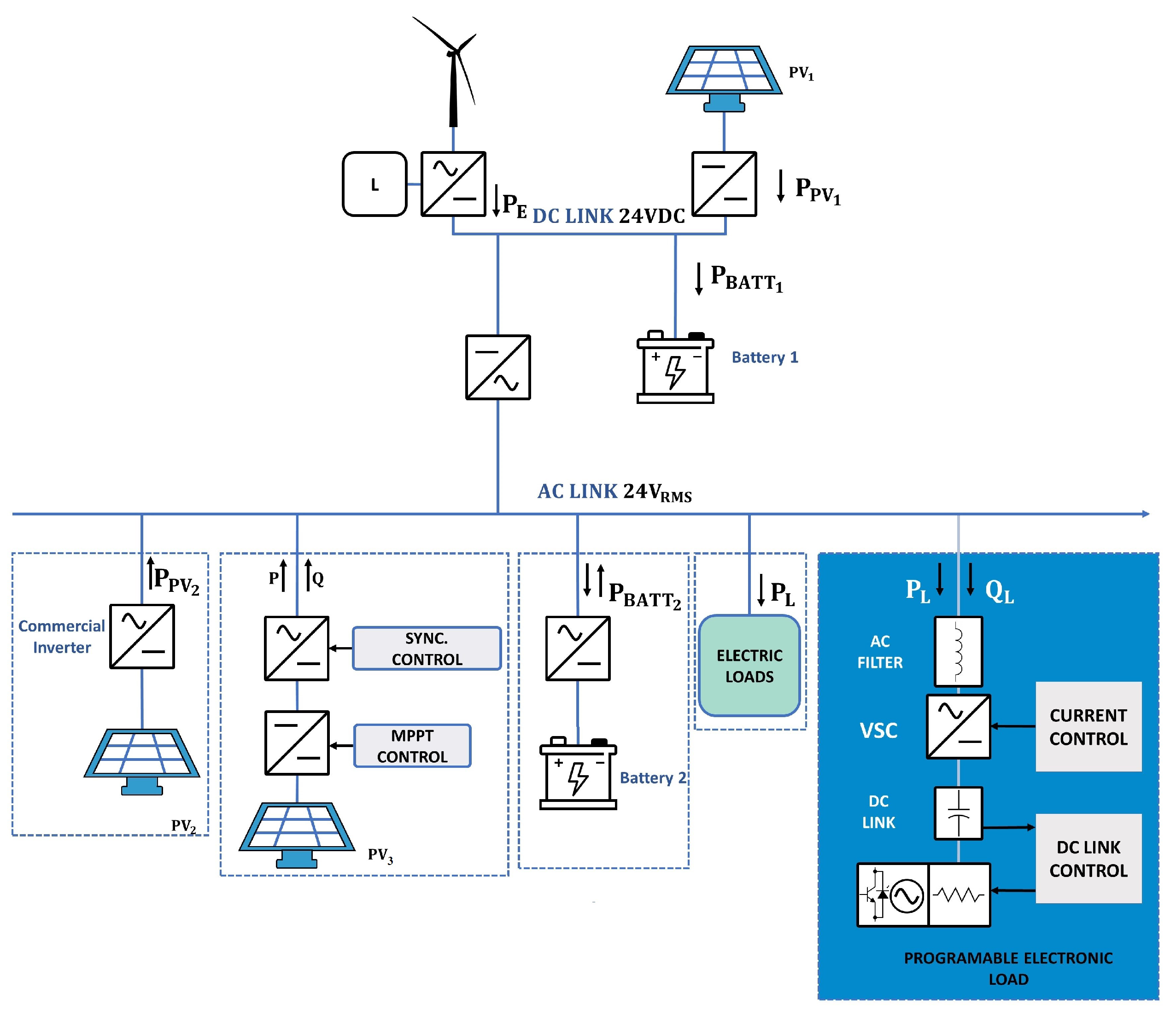
Figure 1.
General diagram of a programmable electronic load (PEL) connected to a microgrid.
Figure 1.
General diagram of a programmable electronic load (PEL) connected to a microgrid.
Figure 2.
AC–DC converter topologies of a PEL. (
a) One-branch converter, (
b) two-branch converter, (
c) three-branch converter, (
d) four-branch converter, and (
e) multilevel converter. Based on [
4].
Figure 2.
AC–DC converter topologies of a PEL. (
a) One-branch converter, (
b) two-branch converter, (
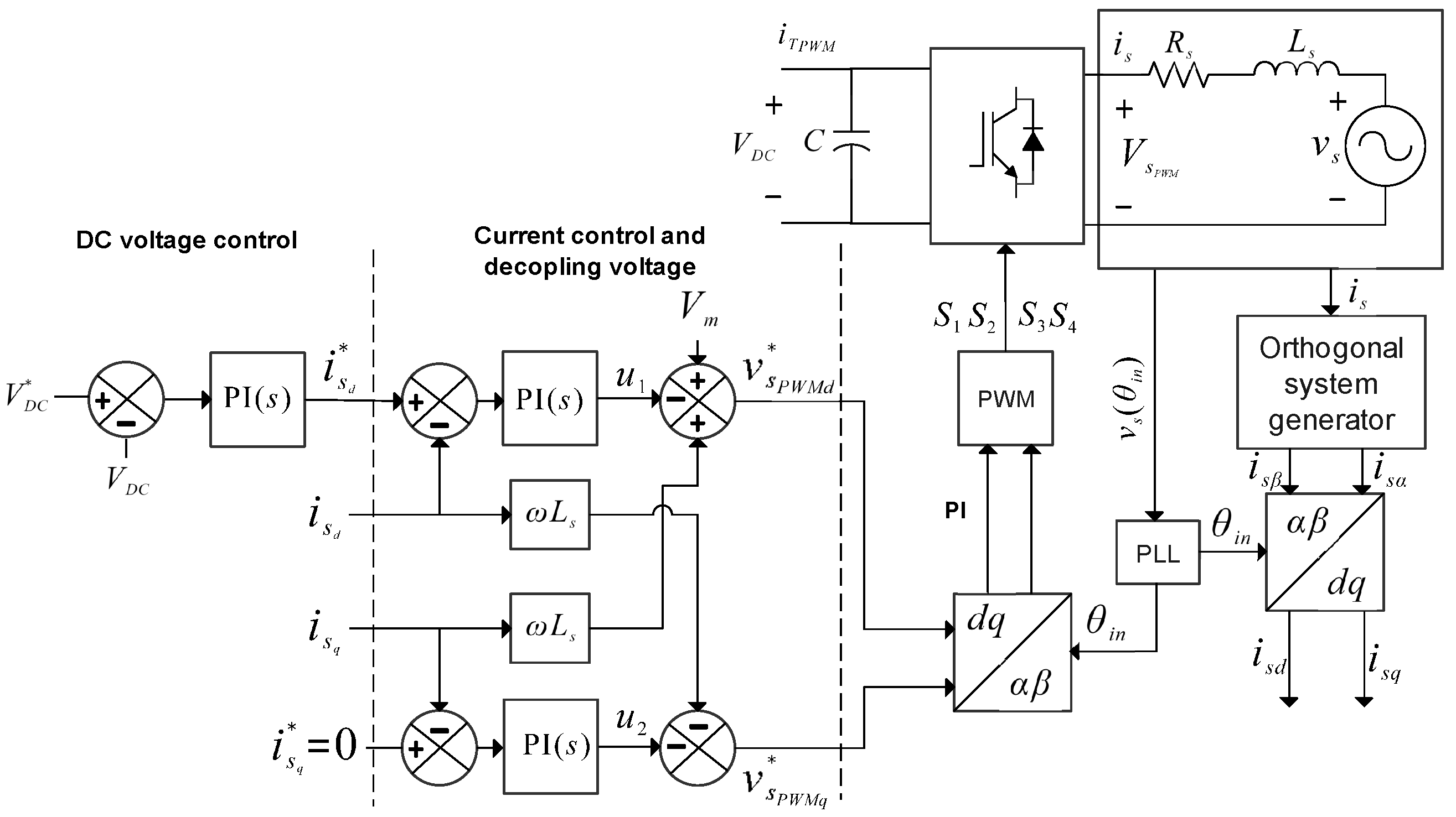
c) three-branch converter, (
d) four-branch converter, and (
e) multilevel converter. Based on [
4].
Figure 3.
Topology of DC power control converters. (a) Power resistor connection in parallel to the capacitor, (b) DC–DC converter, and (c) AC–DC converter.
Figure 3.
Topology of DC power control converters. (a) Power resistor connection in parallel to the capacitor, (b) DC–DC converter, and (c) AC–DC converter.
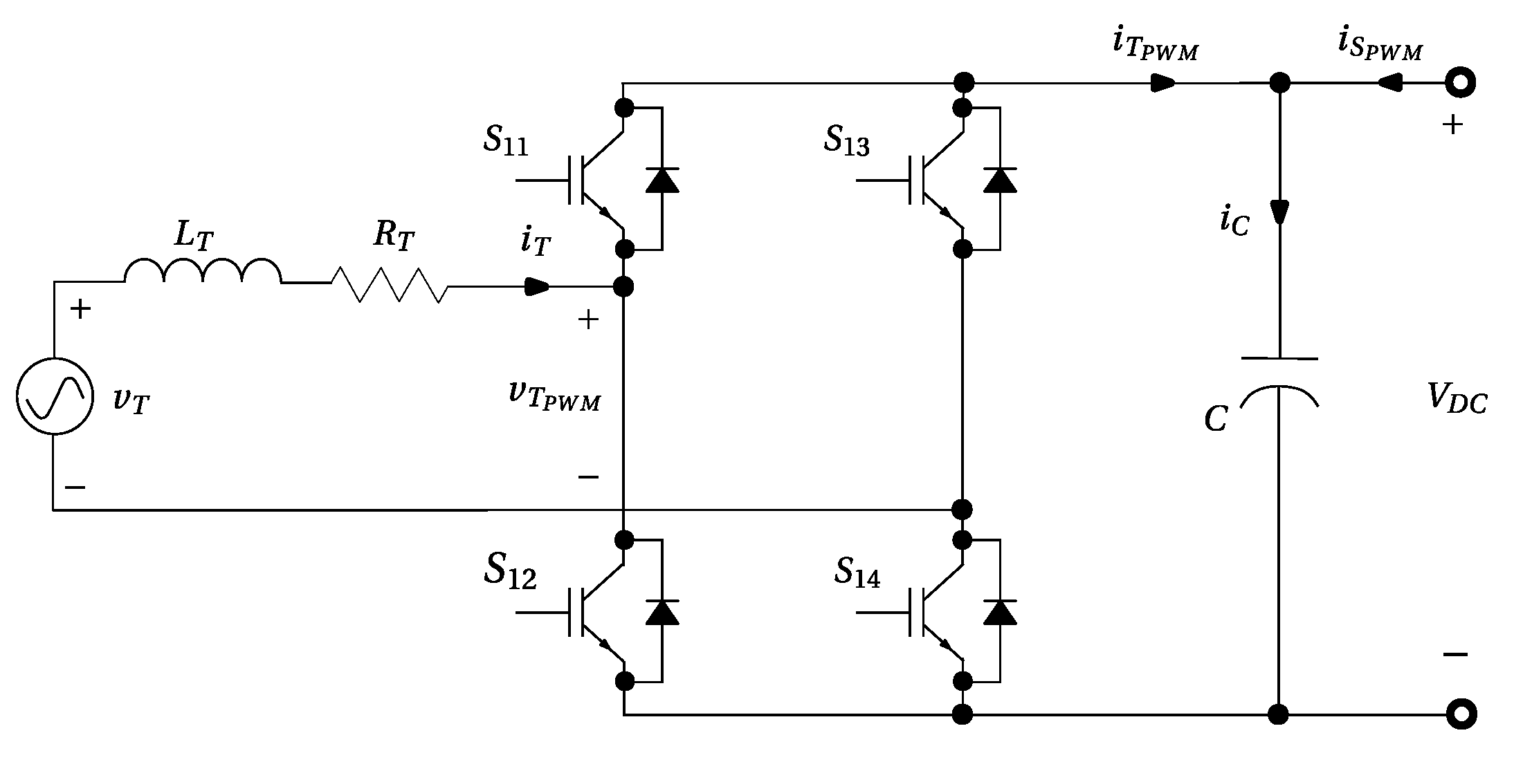
Figure 4.
Power circuit of an AC–DC converter.
Figure 4.
Power circuit of an AC–DC converter.
Figure 5.
Diagram of the PEL connected to a resistive load.
Figure 5.
Diagram of the PEL connected to a resistive load.
Figure 6.
Diagram of the PEL connected to a DC–DC converter.
Figure 6.
Diagram of the PEL connected to a DC–DC converter.
Figure 7.
Power circuit of a DC–AC converter connected to the power grid [
18].
Figure 7.
Power circuit of a DC–AC converter connected to the power grid [
18].
Figure 8.
transform of signal .
Figure 8.
transform of signal .
Figure 9.
Diagram of a single-phase converter connected to the power grid. Based on [
8].
Figure 9.
Diagram of a single-phase converter connected to the power grid. Based on [
8].
Figure 10.
Diagram of the PEL connected to a single-phase DC-AC converter. Based on [
8].
Figure 10.
Diagram of the PEL connected to a single-phase DC-AC converter. Based on [
8].
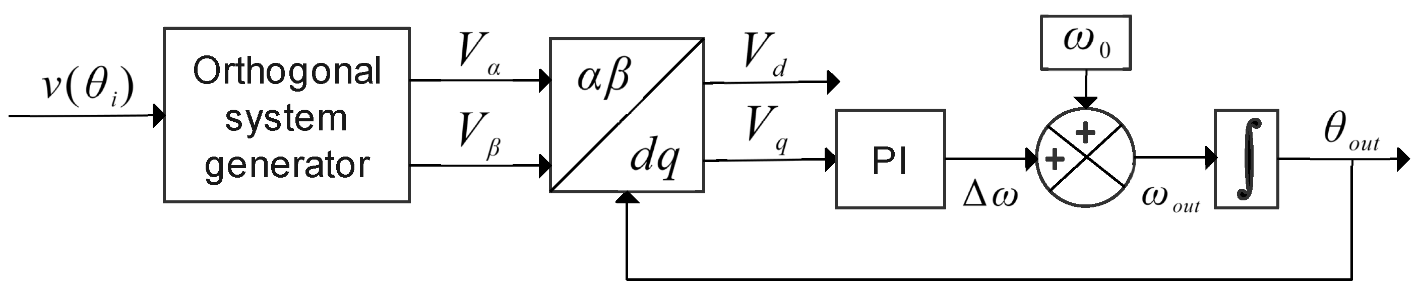
Figure 11.
Basic structure of a single-phase SRF-PLL.
Figure 11.
Basic structure of a single-phase SRF-PLL.
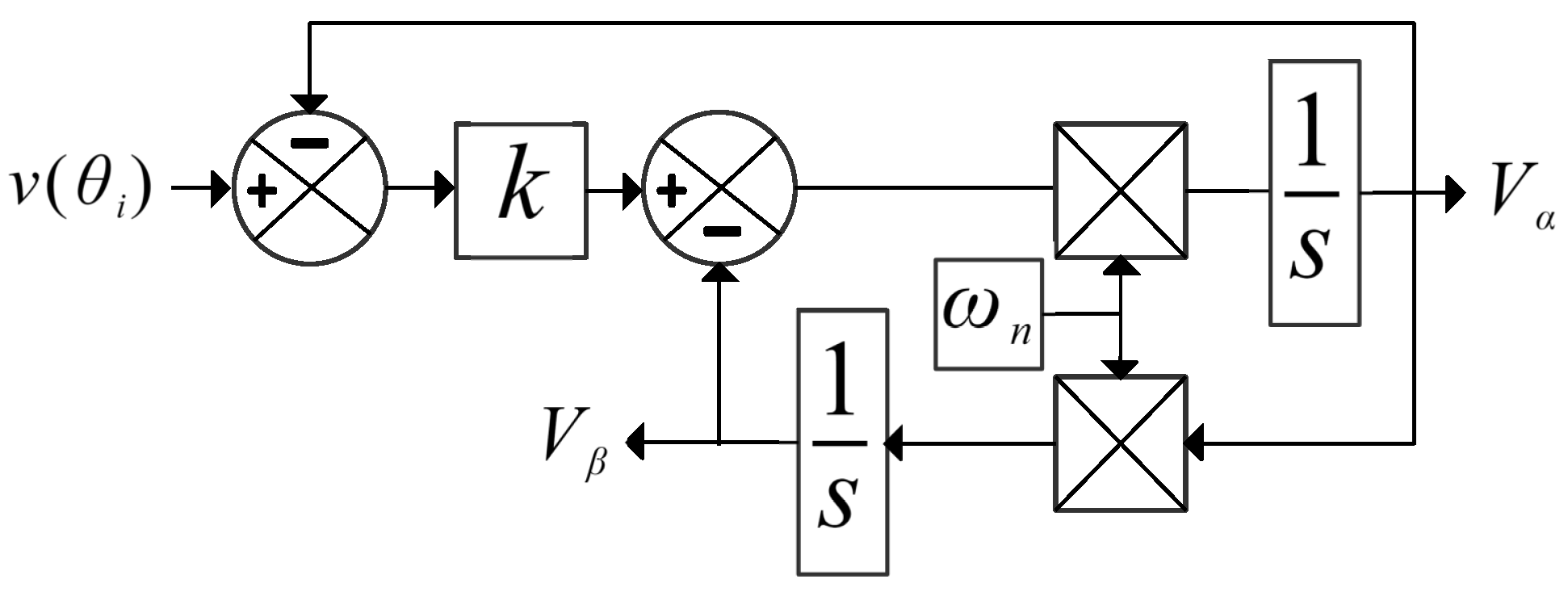
Figure 12.
Second-order generalized integrator scheme (SOGI).
Figure 12.
Second-order generalized integrator scheme (SOGI).
Figure 13.
PLL structure simplification.
Figure 13.
PLL structure simplification.
Figure 14.
Hysteresis control scheme.
Figure 14.
Hysteresis control scheme.
Figure 15.
General diagram of programmable electronic load with a DC–DC converter and a load resistance.
Figure 15.
General diagram of programmable electronic load with a DC–DC converter and a load resistance.
Figure 16.
Control diagram for a converter connected to the power grid.
Figure 16.
Control diagram for a converter connected to the power grid.
Figure 17.
General diagram of programmable electronic load with DC-AC converter and reinjection to the AC power grid.
Figure 17.
General diagram of programmable electronic load with DC-AC converter and reinjection to the AC power grid.
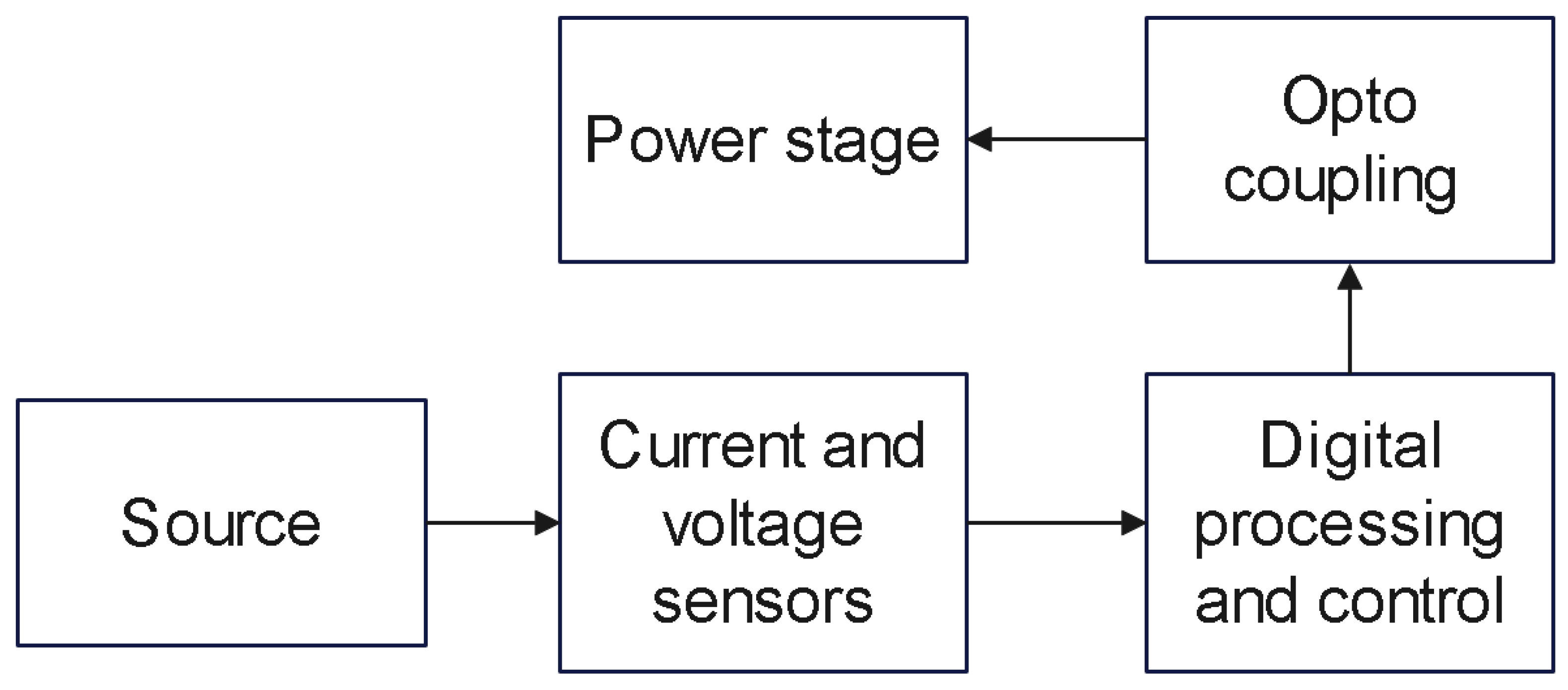
Figure 18.
Diagram of the implementation stages.
Figure 18.
Diagram of the implementation stages.
Figure 19.
Implementation of the device.
Figure 19.
Implementation of the device.
Figure 20.
AC voltage sensor.
Figure 20.
AC voltage sensor.
Figure 21.
Output current sensor.
Figure 21.
Output current sensor.
Figure 22.
Sensing process and output current control.
Figure 22.
Sensing process and output current control.
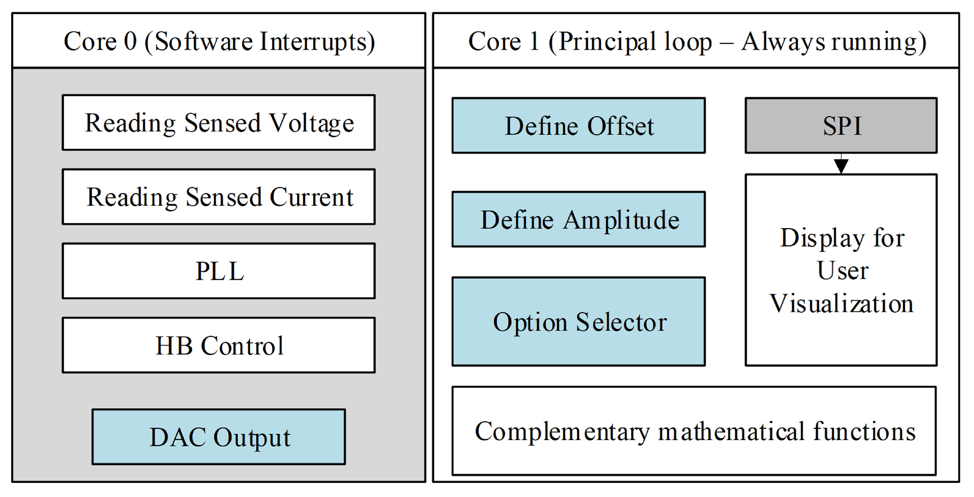
Figure 23.
Parallel tasks assigned to each ESP32 core.
Figure 23.
Parallel tasks assigned to each ESP32 core.
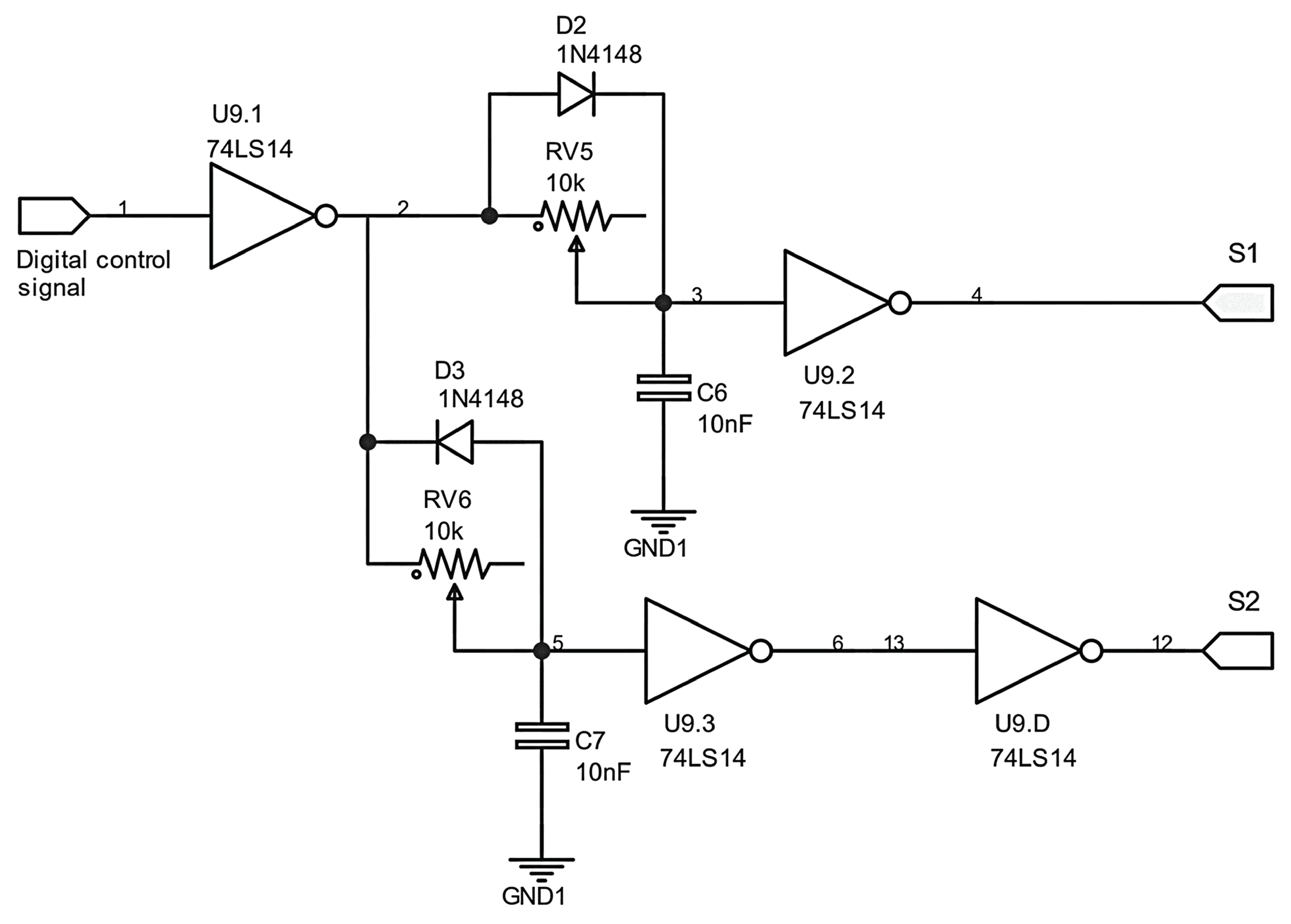
Figure 24.
Diagram of a dead time generator circuit. Based on [
23].
Figure 24.
Diagram of a dead time generator circuit. Based on [
23].
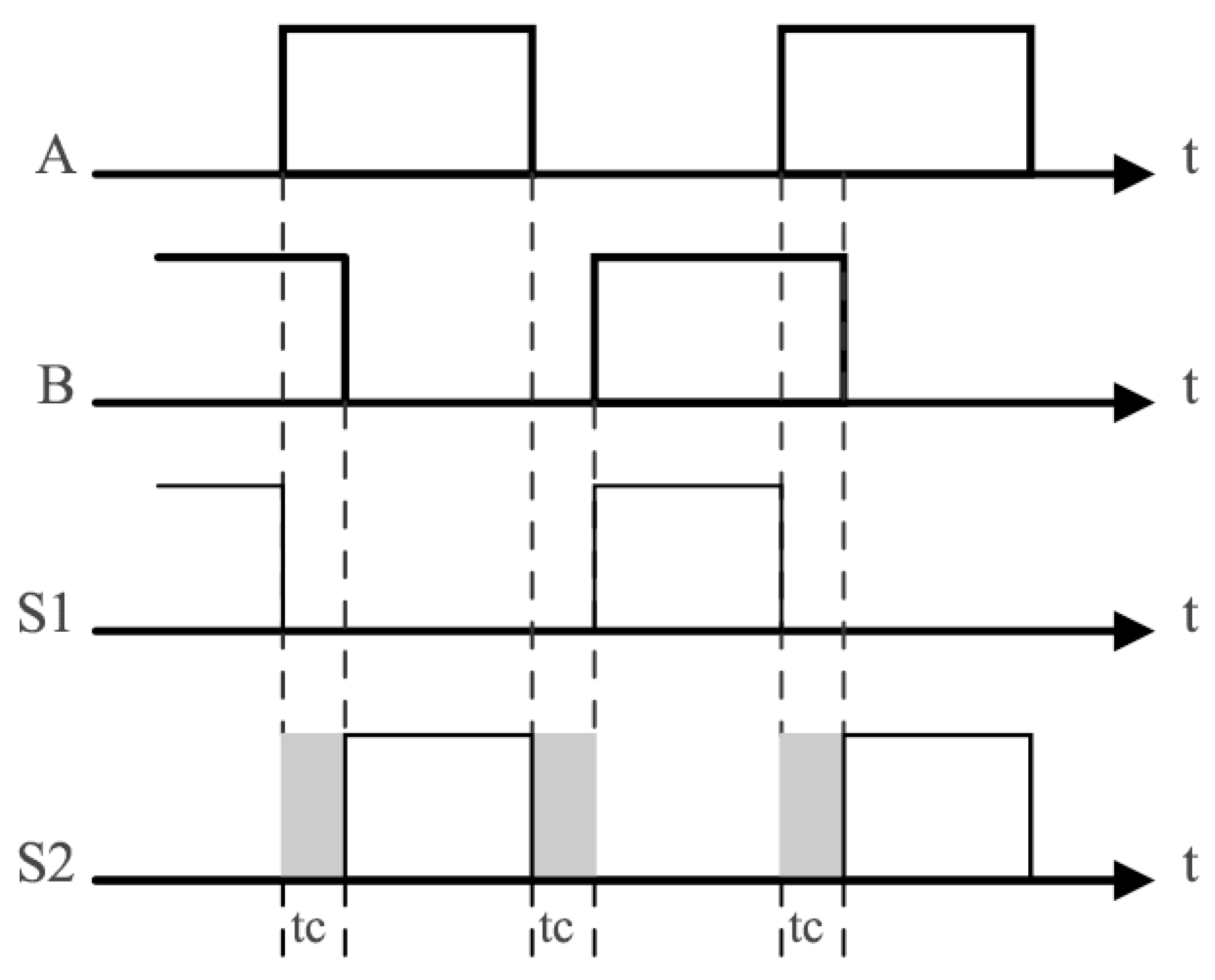
Figure 25.
Waveforms in the dead time generator. Based on [
23].
Figure 25.
Waveforms in the dead time generator. Based on [
23].
Figure 26.
Design of the dead time generator circuit implemented in the digital control for current and the DC link.
Figure 26.
Design of the dead time generator circuit implemented in the digital control for current and the DC link.
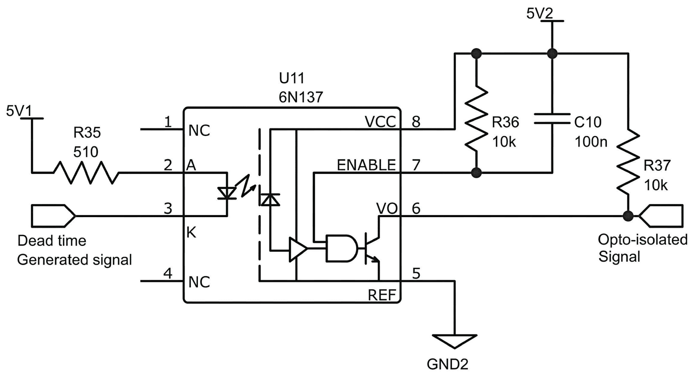
Figure 27.
Electronic design of the optocoupler stage of digital output.
Figure 27.
Electronic design of the optocoupler stage of digital output.
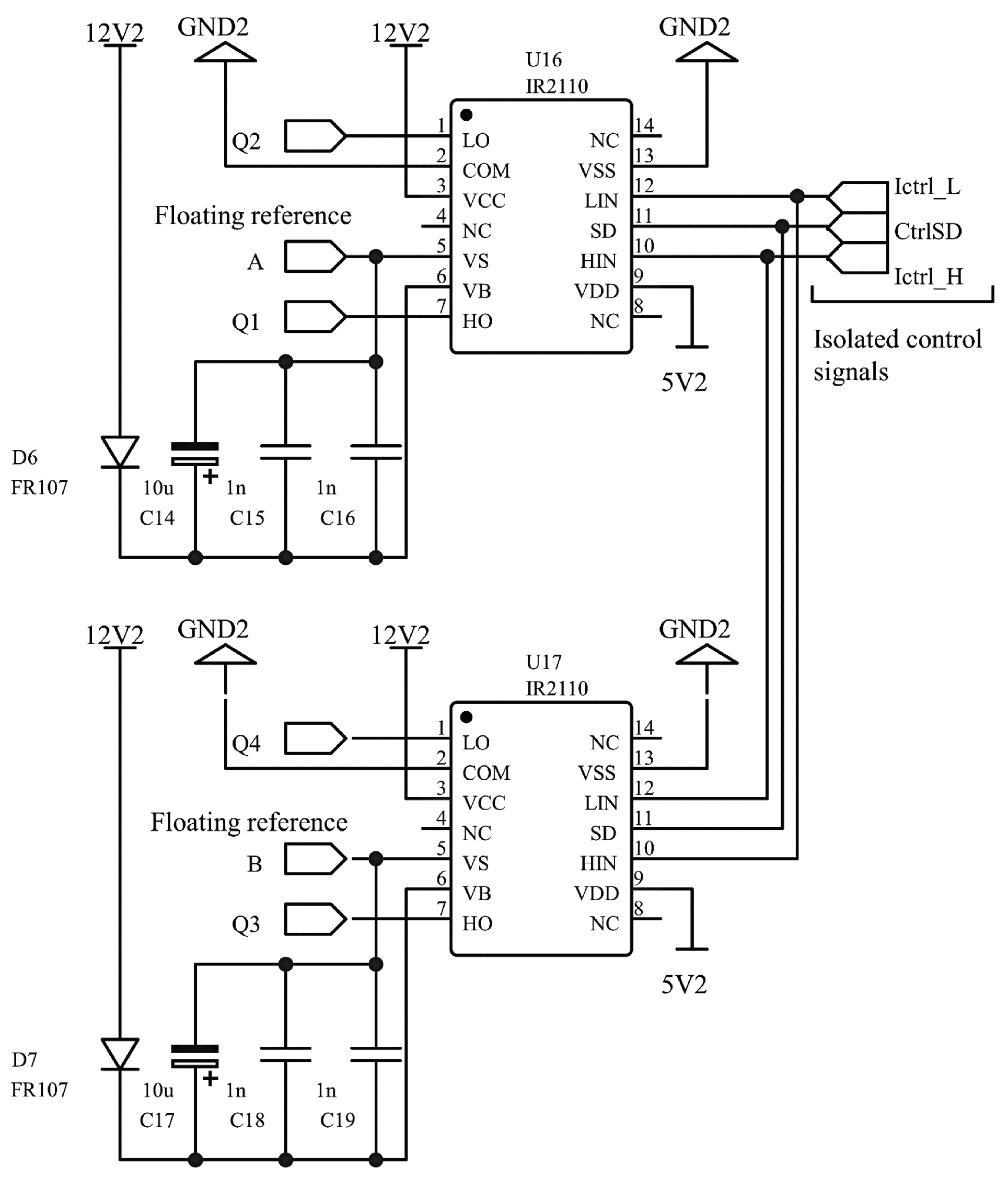
Figure 28.
Design of the optocoupler for digital control of the power driver.
Figure 28.
Design of the optocoupler for digital control of the power driver.
Figure 29.
General diagram of the power stage.
Figure 29.
General diagram of the power stage.
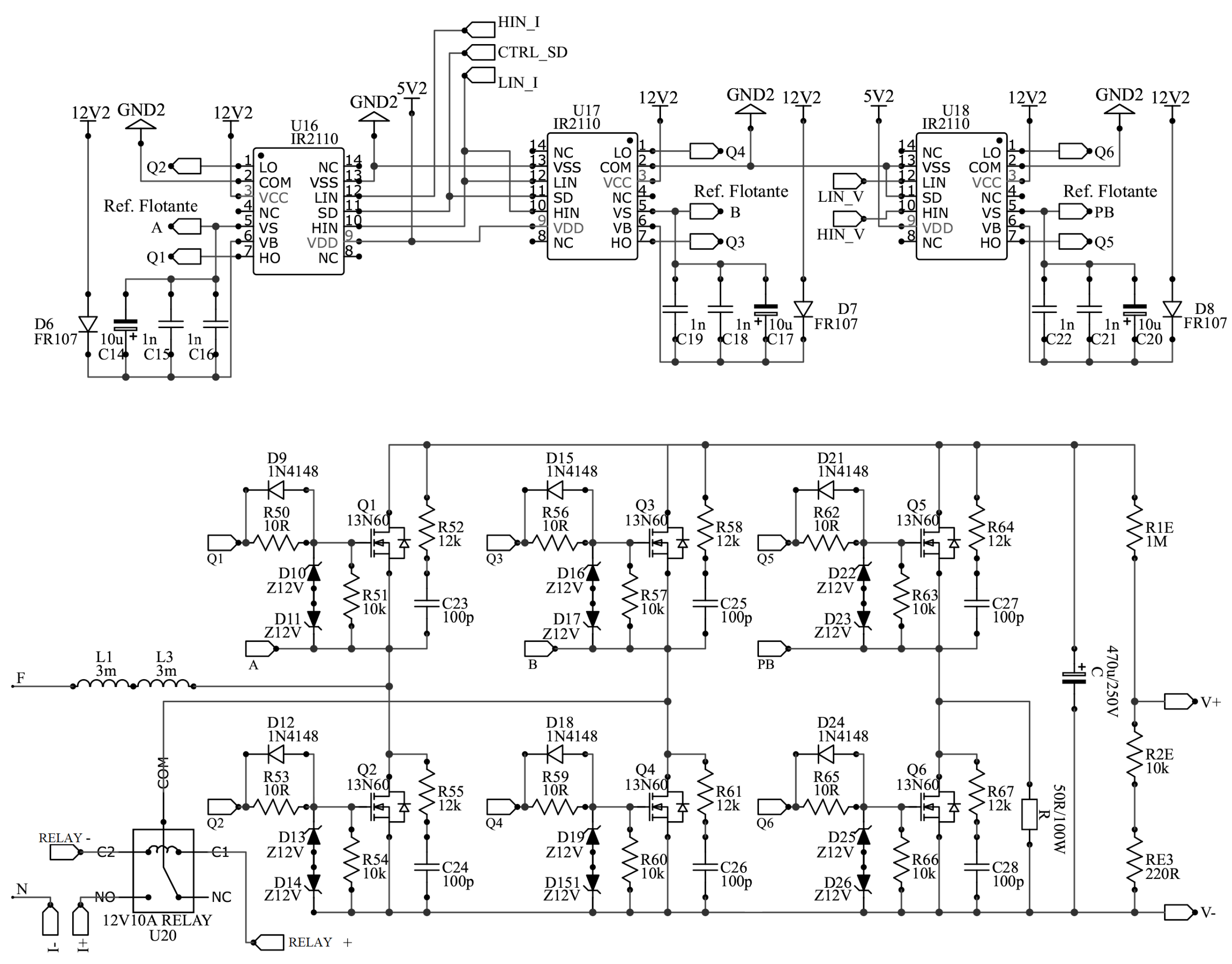
Figure 30.
Circuit design for the control of power transistors using IR2110 drivers.
Figure 30.
Circuit design for the control of power transistors using IR2110 drivers.
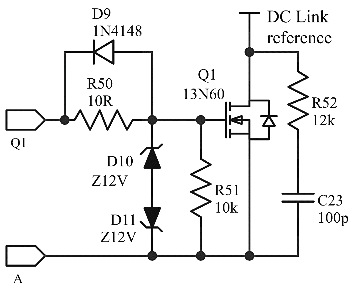
Figure 31.
Design of the protections implemented to each MOSFET transistor.
Figure 31.
Design of the protections implemented to each MOSFET transistor.
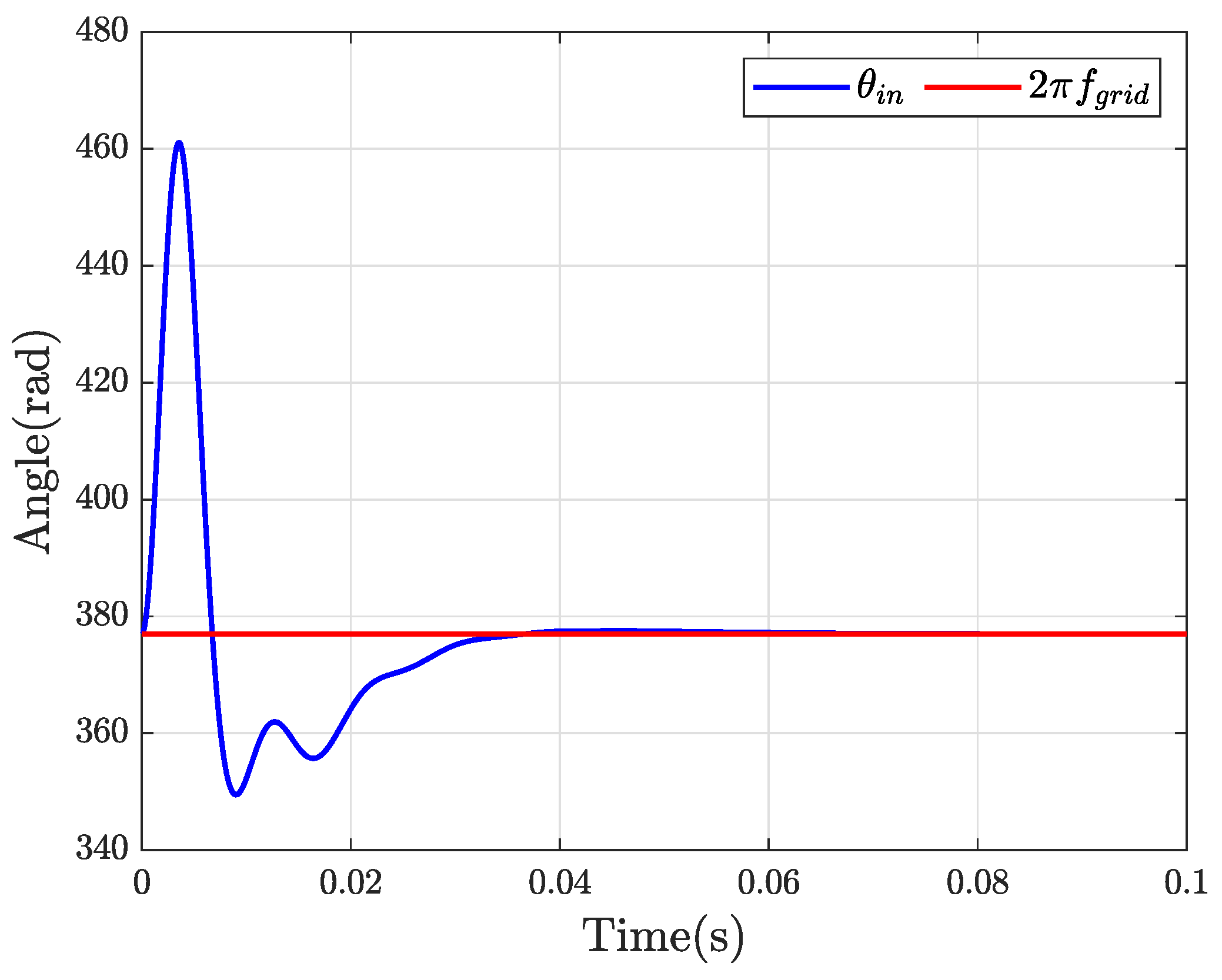
Figure 32.
Time response of the designed PLL.
Figure 32.
Time response of the designed PLL.
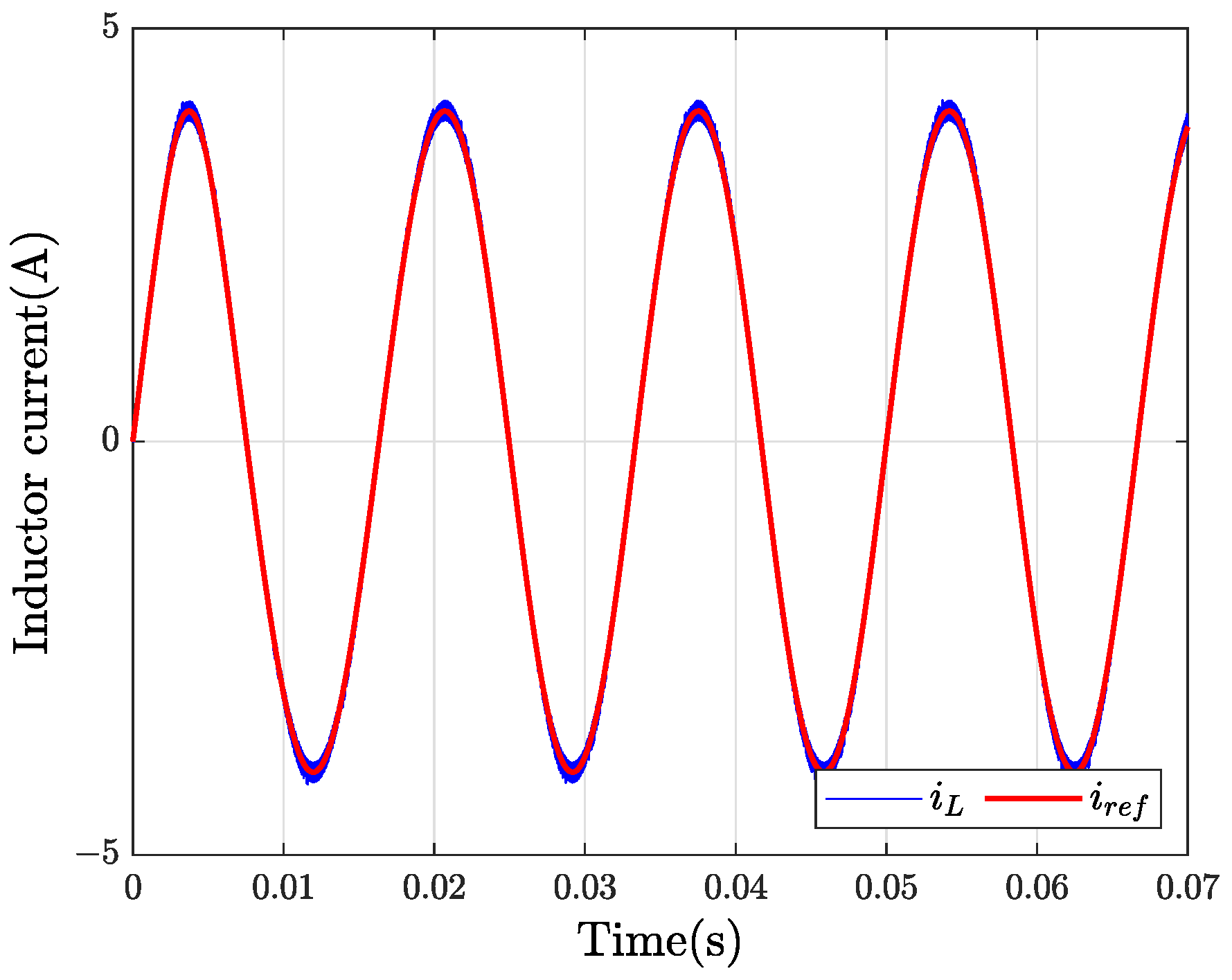
Figure 33.
Inductor current and grid voltage measured in the PEL.
Figure 33.
Inductor current and grid voltage measured in the PEL.
Figure 34.
DC link voltage measured across the capacitor.
Figure 34.
DC link voltage measured across the capacitor.
Figure 35.
Output current measured in the inductor of the PEL. (a) Resistive load emulation with A, A and A. (b) Inductive and capacitive load emulation considering changes: , and . (c) Nonlinear load emulation for , , and .
Figure 35.
Output current measured in the inductor of the PEL. (a) Resistive load emulation with A, A and A. (b) Inductive and capacitive load emulation considering changes: , and . (c) Nonlinear load emulation for , , and .
Figure 36.
DC link output for V, V and V, measured on the capacitor.
Figure 36.
DC link output for V, V and V, measured on the capacitor.
Figure 37.
(a,b) PEL output current measured in the inductor for a resistive load with A and A, .
Figure 37.
(a,b) PEL output current measured in the inductor for a resistive load with A and A, .
Figure 38.
(a,b) PEL output current measured in the inductor for an inductive load with and capacitive , A.
Figure 38.
(a,b) PEL output current measured in the inductor for an inductive load with and capacitive , A.
Figure 39.
(a,b) PEL output current measured in the inductor for a nonlinear load.
Figure 39.
(a,b) PEL output current measured in the inductor for a nonlinear load.
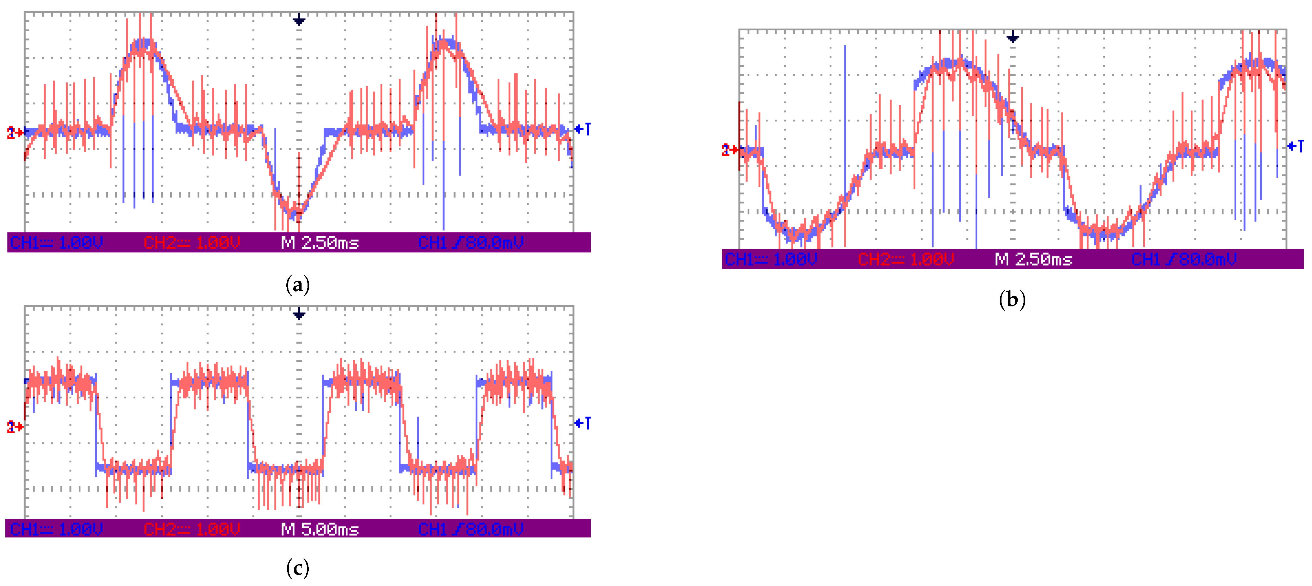
Figure 40.
(a,b) DC–AC converter working as inverter for a , , and A.
Figure 40.
(a,b) DC–AC converter working as inverter for a , , and A.
Figure 41.
DC link response for V.
Figure 41.
DC link response for V.
Figure 42.
Output current of the PEL when s.
Figure 42.
Output current of the PEL when s.
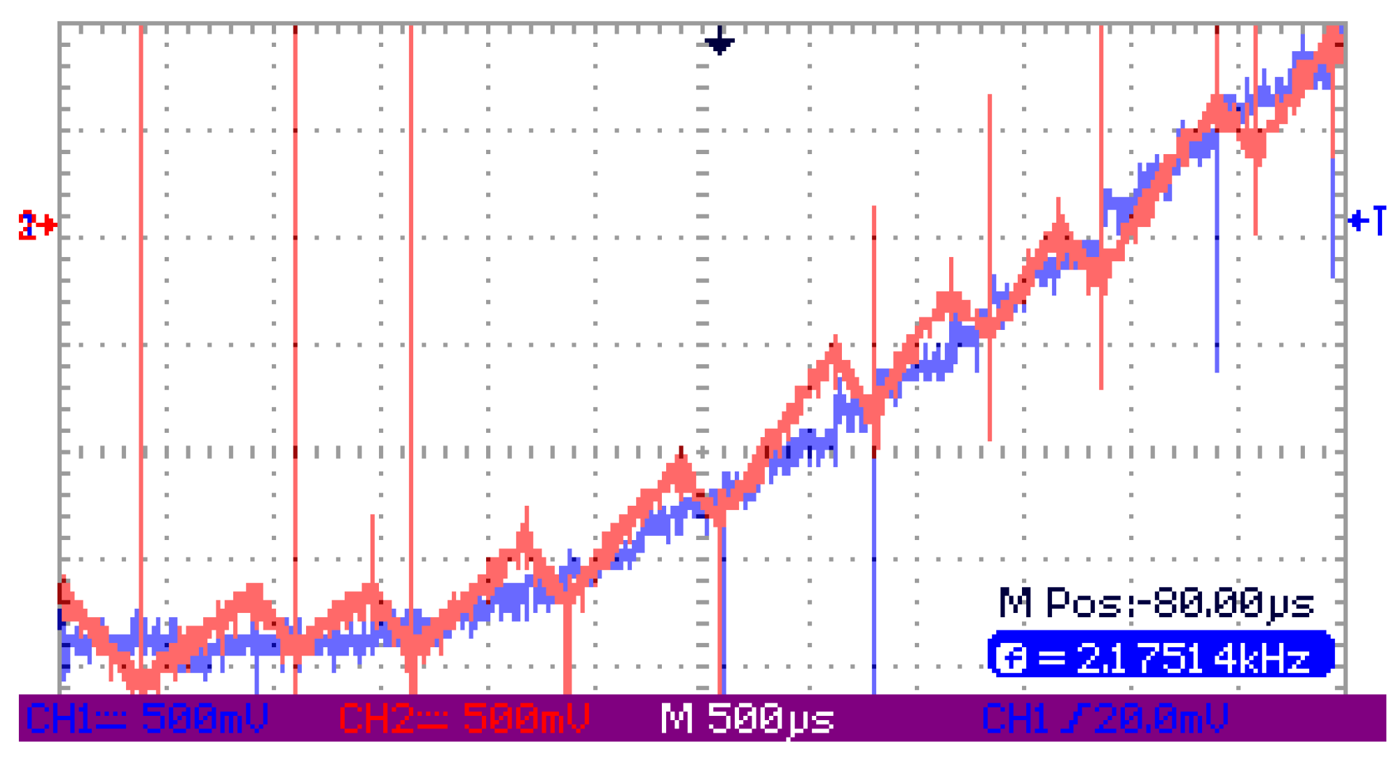
Figure 43.
Effects of on the output current of the PEL for s.
Figure 43.
Effects of on the output current of the PEL for s.
Figure 44.
Effects of on the output current of the PEL for s.
Figure 44.
Effects of on the output current of the PEL for s.
Figure 45.
General scheme of the implemented PEL.
Figure 45.
General scheme of the implemented PEL.
Figure 46.
User interface to enter the parameters for load emulation.
Figure 46.
User interface to enter the parameters for load emulation.
Figure 47.
Reference signals generated by the microcontroller. (a) Nonlinear current signal generated with A and . (b) Nonlinear current signal generated with A and . (c) Linear current signal generated with A and .
Figure 47.
Reference signals generated by the microcontroller. (a) Nonlinear current signal generated with A and . (b) Nonlinear current signal generated with A and . (c) Linear current signal generated with A and .
Figure 48.
Emulation of linear loads. (a) Resistive load generated by the prototype with A and . (b) Capacitive load generated by the prototype with A and . (c) Inductive load generated by the prototype with A and .
Figure 48.
Emulation of linear loads. (a) Resistive load generated by the prototype with A and . (b) Capacitive load generated by the prototype with A and . (c) Inductive load generated by the prototype with A and .
Figure 49.
Current measurement for emulation of nonlinear loads. (a) Nonlinear load emulation with A and . (b) Nonlinear load emulation with A and . (c) Emulation of a square wave current load with A.
Figure 49.
Current measurement for emulation of nonlinear loads. (a) Nonlinear load emulation with A and . (b) Nonlinear load emulation with A and . (c) Emulation of a square wave current load with A.
Figure 50.
Inductor current following the reference signal.
Figure 50.
Inductor current following the reference signal.
Table 1.
Advantages and disadvantages of AC–DC topologies.
Table 1.
Advantages and disadvantages of AC–DC topologies.
| AC–DC Converter | Advantages | Disadvantages |
|---|
| One branch | This device is easy to control and implement in single-phase systems. It has only two power switches and a small number of trigger circuits. | It has only two DC links and requires components that support higher voltage and power balance control in both capacitors. |
| Two branches | This device is easy to control and implement in single-phase systems. It uses better the DC link, and the voltage supported by the switches is half that of the one-branch topology. | The number of switches is doubled concerning the one-branch AC–DC converter. Thus, more switches represent a greater number of trigger circuits. |
| Three branches | It is the most commonly used in three-phase systems. It handles higher power and voltage, allowing lower losses in power switches than one- and two-branch topologies. | The number of switches increases, and an additional trigger circuit is required, bringing more implementation difficulties. |
| Four branches | In three-phase systems, the number of applications increases because it controls each phase and the neutral of AC sources. | It is more difficult to implement because the number of switches increases, and more trigger circuits are needed. |
| Multilevel | It can be implemented for both single-phase and three-phase systems. It handles greater power compared to other topologies. A better quality of the current waveform and low harmonic distortion is obtained, a lower switching frequency is needed, and the number and order of filters are redefined. | The complexity of the controller and its implementation increases because of the greater number of switches. |
Table 2.
Advantages and disadvantages of DC control links.
Table 2.
Advantages and disadvantages of DC control links.
| Link | Advantages | Disadvantages |
|---|
| Parallel Resistor | It is the simplest way to split power and does not need a DC link voltage control; therefore, it is easy to implement. | It limits the operating power range of the system. |
| DC–DC converter | A greater operation range is obtained compared to the previous topology. Although components are increased, it is easy to control and implement. | Compared to the previous topology, the number of components increases, and it needs a control stage. It depends on a load resistance and is limited by its maximum operating values. |
| AC–DC voltage inverter | This configuration handles much higher powers as it does not depend on load resistance. It allows bidirectional control of the power flow by operating in the entire range of the P-Q plane. | As the number of components increases, more difficult controls are needed for implementation. It depends on the availability of the receptive AC power grid. |
Table 3.
Parameters for the PEL connected to a resistive load.
Table 3.
Parameters for the PEL connected to a resistive load.
| Parameter | Value |
|---|
| 6 mH |
| 2 |
| C | 470 F |
| 200 |
Table 4.
Parameters for the PEL connected to a DC–DC converter.
Table 4.
Parameters for the PEL connected to a DC–DC converter.
| Parameter | Value |
|---|
| 6 mH |
| 2 |
| C | 470 F |
| 100 |
Table 5.
Parameters of the PEL connected to a DC–AC converter.
Table 5.
Parameters of the PEL connected to a DC–AC converter.
| Parameter | Value |
|---|
| 10 mH |
| 3 |
| C | 3300 F |
| 6 mH |
| 2 |
| 400 V |
| 120 V |
| 120 V |
Table 6.
Validation of the reference signal generation.
Table 6.
Validation of the reference signal generation.
| | Parameter |
|---|
| | Reference | Measured |
| 1.0 | 1.16 |
| 1.5 | 1.65 |
| 2 | 2.2 |
| 3 | 3.16 |
| −60 | −59.84 |
| −45 | −46.4 |
| 0 | 0.26 |
| 45 | 46.26 |
| 80 | 81.36 |
| 30 | 31.31 |
| 90 | 95.24 |
| 120 | 125.44 |
| 160 | 155.2 |


 ,
, 


