
Thermal Sensors for Contactless Temperature Measurements, Occupancy Detection, and Automatic Operation of Appliances during the COVID-19 Pandemic: A Review


Abstract
:1. Introduction
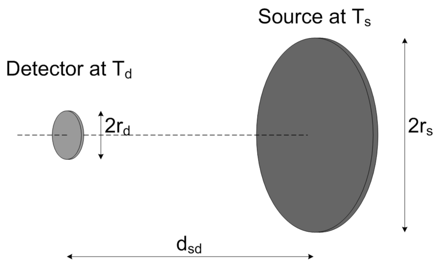
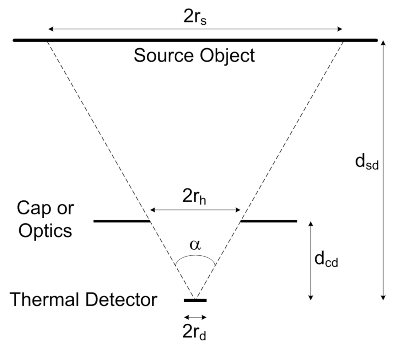
2. Thermal Detectors Theory
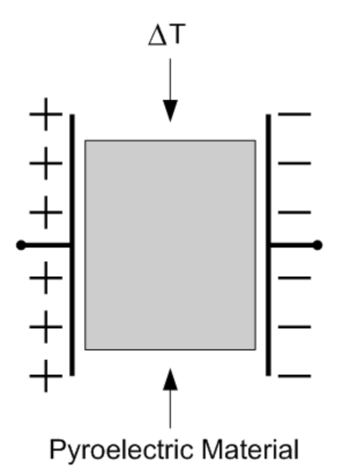
2.1. Bolometers
2.2. Pyrometers
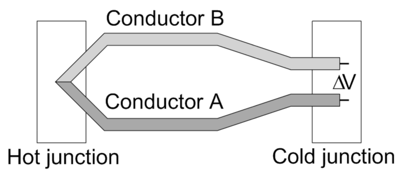
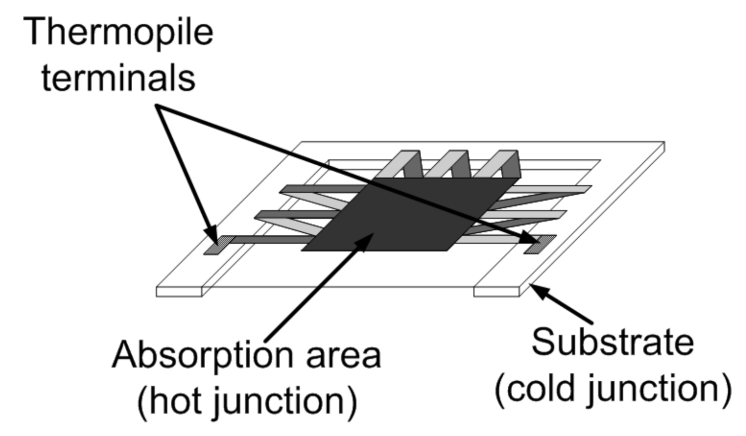
2.3. Thermopiles
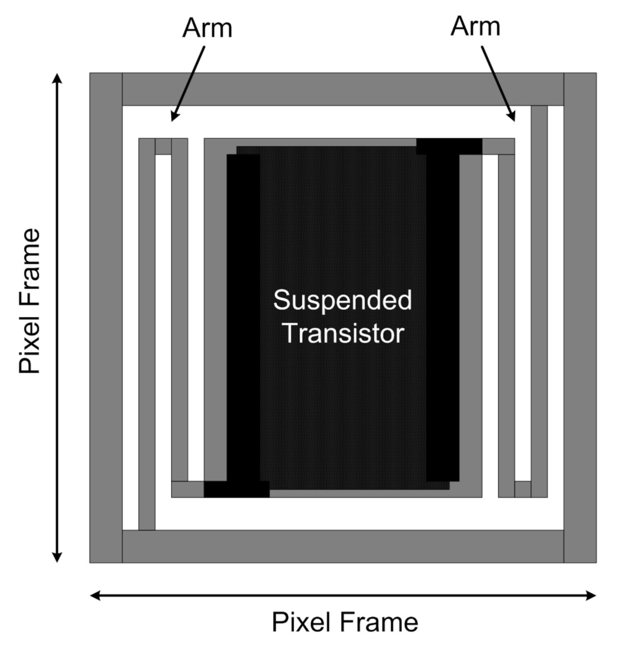
2.4. TMOS
3. State-of-the-Art Review
3.1. Bolometers
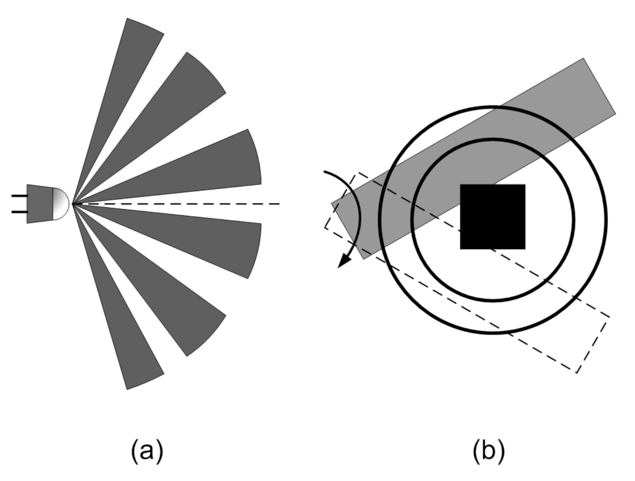
3.2. Pyrometers
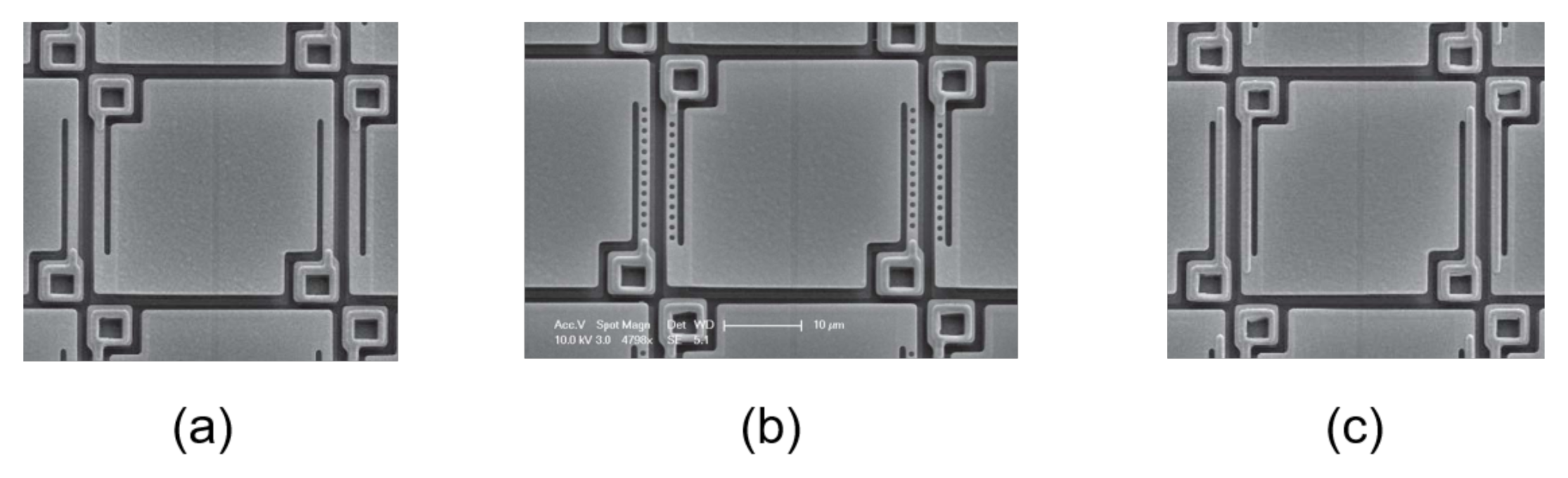
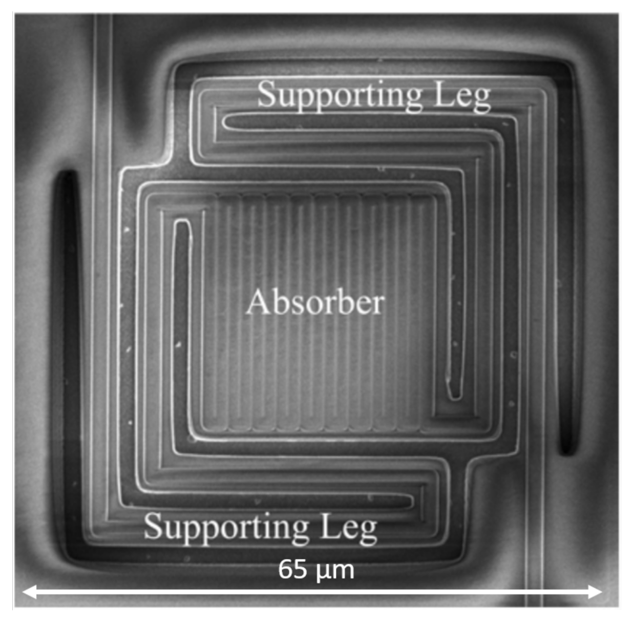
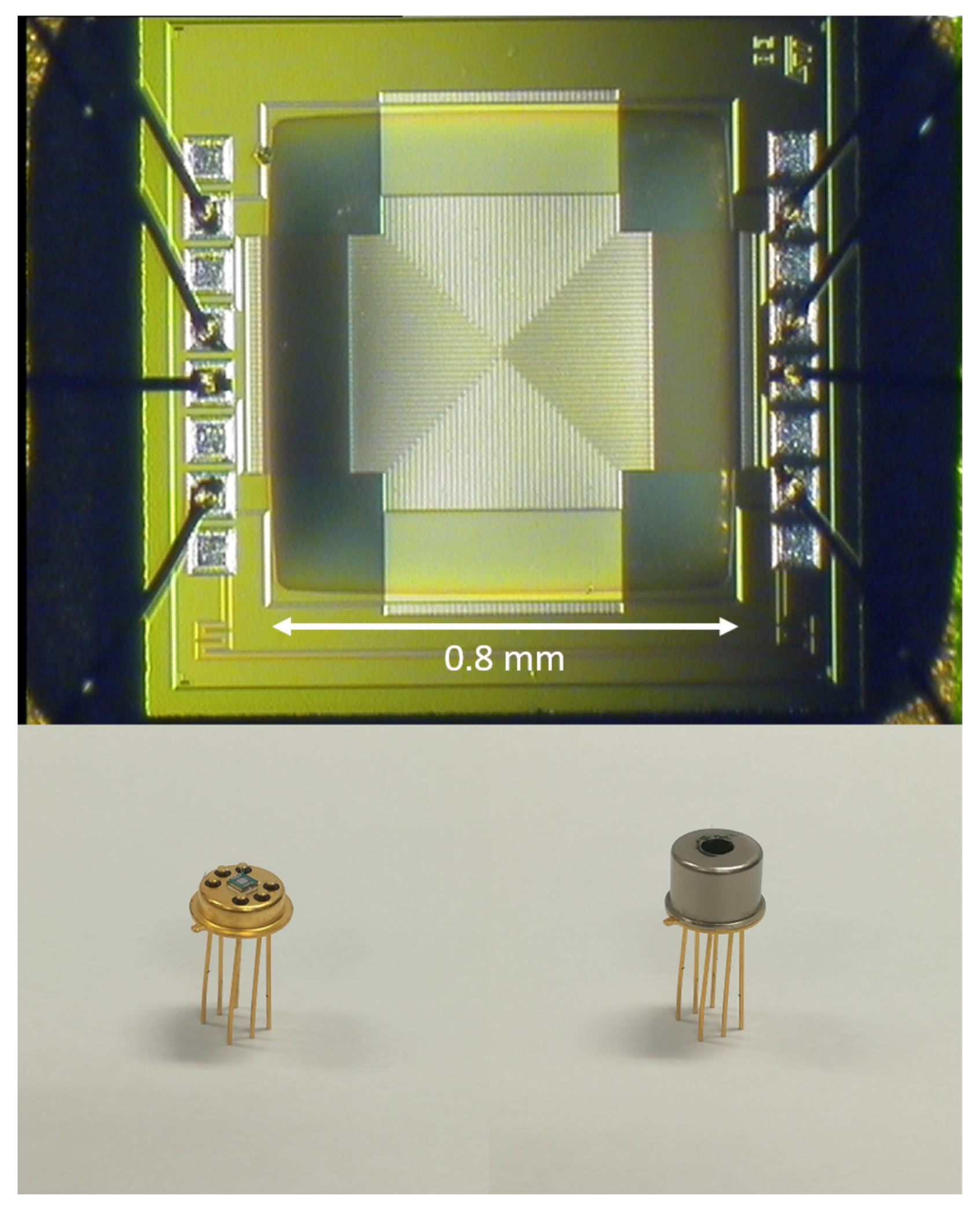
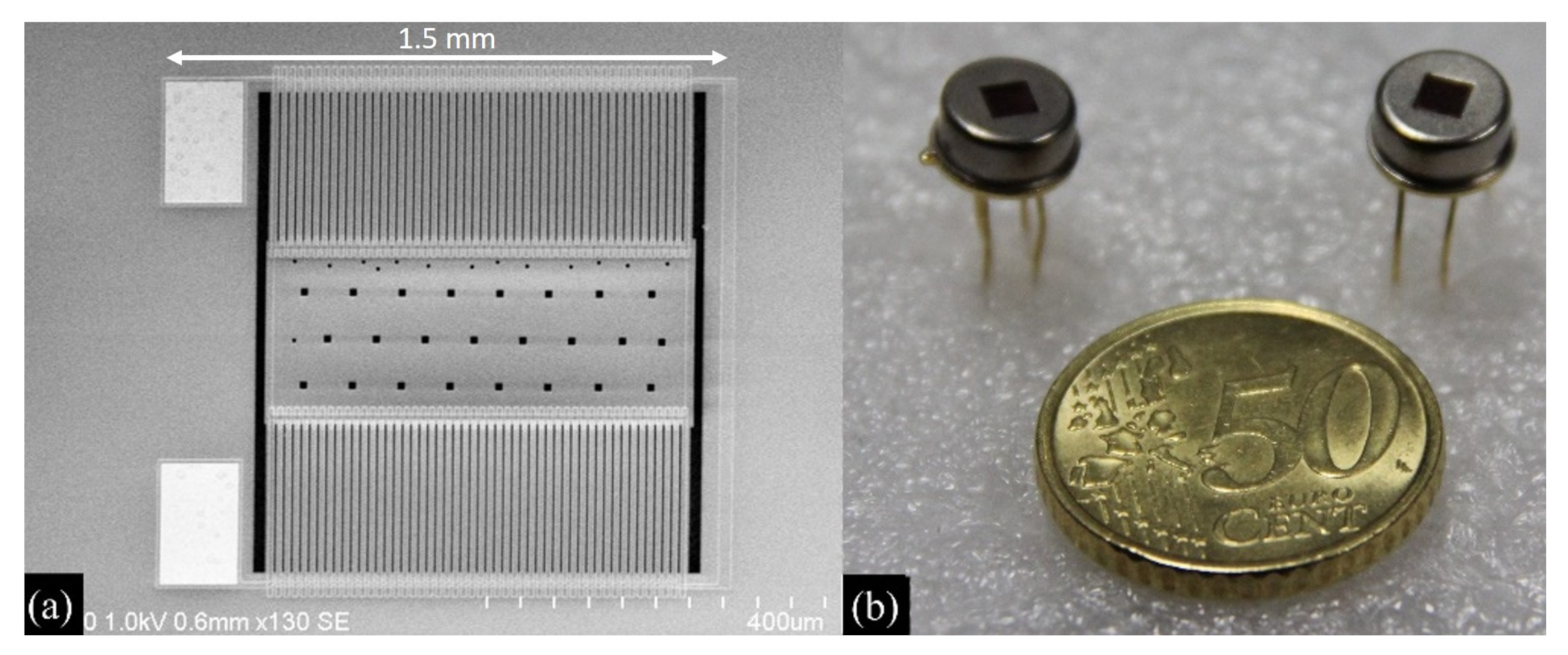
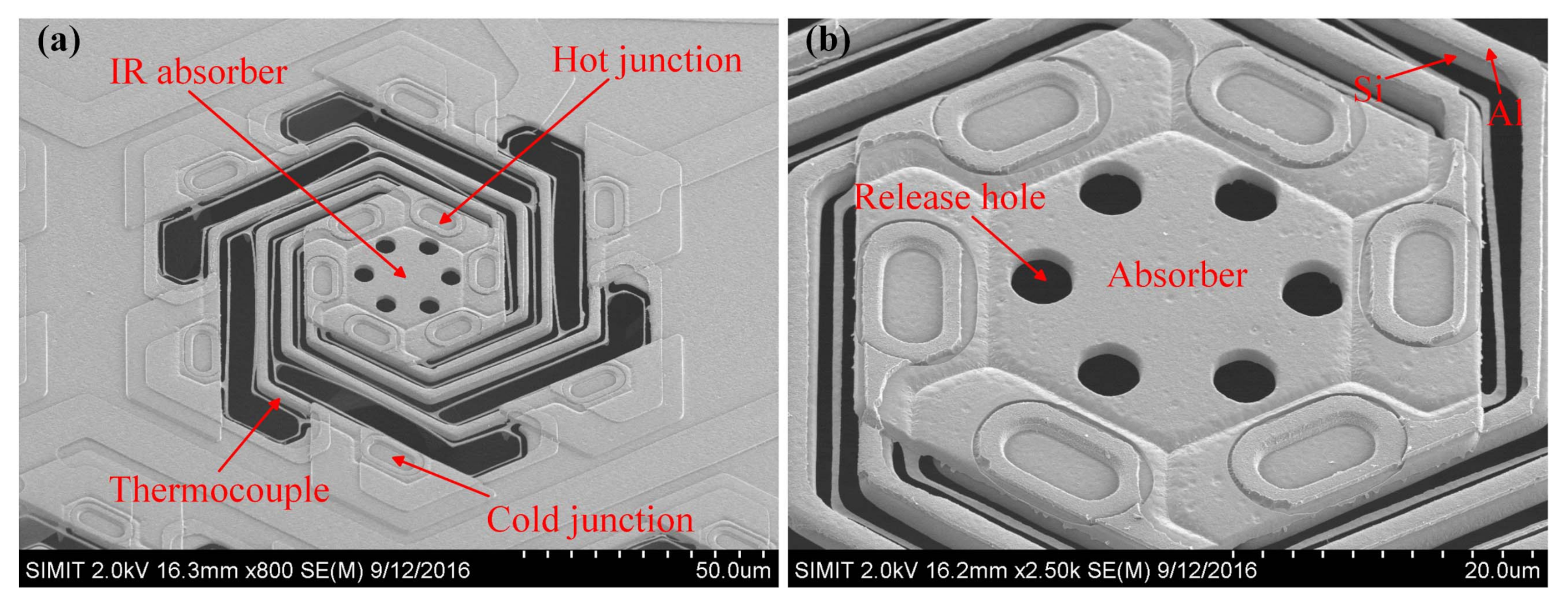
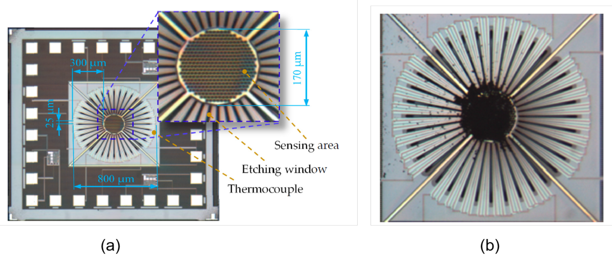
3.3. Thermopiles
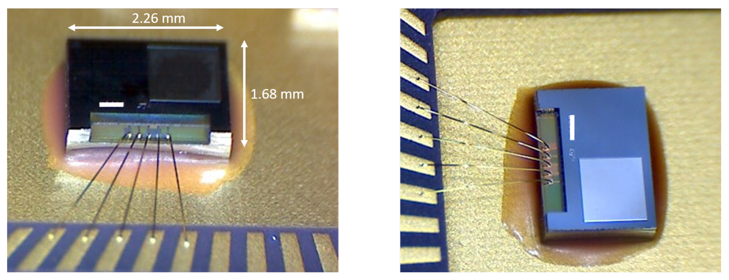
3.4. TMOS
4. Conclusions
Author Contributions
Funding
Conflicts of Interest
References
- Randjelović, D.V. Analytical Modelling Approach in Study of the Transient Response of Thermopile-Based MEMS Sensors Applied for Simultaneous Detection of Pressure and Gas Composition. In Proceedings of the 2018 International Semiconductor Conference (CAS), Sinaia, Romania, 10–12 October 2018; pp. 27–34. [Google Scholar] [CrossRef]
- Xue, D.; Song, F.; Wang, J.; Li, X. Single-Side Fabricated p+Si/Al Thermopile-Based Gas Flow Sensor for IC-Foundry-Compatible, High-Yield, and Low-Cost Volume Manufacturing. IEEE Trans. Electron Devices 2019, 66, 821–824. [Google Scholar] [CrossRef]
- Wang, S.; Wang, J.; Li, X. Sensitivity Improvement of P+Si/Au Thermopile-Based Gas Flow Sensor by Optimizing Heat-Sink and Thermal-Insulation Configuration. In Proceedings of the 2020 IEEE 33rd International Conference on Micro Electro Mechanical Systems (MEMS), Vancouver, BC, Canada, 18–22 January 2020. [Google Scholar]
- Linzmeier, D. Pedestrian detection with thermopiles using an occupancy grid. In Proceedings of the 7th International IEEE Conference on Intelligent Transportation Systems, Washington, WA, USA, 3–6 October 2004. [Google Scholar]
- Linzmeier, D.; Koestler, A.; Mekhaiel, M.; Dietmayer, K.C.J. Simulation of thermopile IR-Sensors for Automotive Safety Applications. In Proceedings of the IEEE 63rd Vehicular Technology Conference, Melbourne, Australia, 7–10 May 2006. [Google Scholar]
- Liess, M.; Hausner, M.; Schilz, J.; Lauck, G.; Karagoezoglu, H.; Ernst, H. Temperature radiation sensors for automotive climate control. In Proceedings of the IEEE Sensors Conference, Vienna, Austria, 24–27 October 2004. [Google Scholar]
- Mariani, G.; Kenyon, M. Room-temperature remote sensing: Far-infrared imaging based on thermopile technology. In Proceedings of the 2015 40th International Conference on Infrared, Millimeter and Terahertz waves (IRMMW-THz), Hong Kong, China, 23–28 August 2015. [Google Scholar]
- Datasheet of TS118-3 Thermopile Sensor by Measurement Specialties. Available online: http://lusosat.org/hardware/200612916515751780.pdf (accessed on 2 January 2021).
- Datasheet of ZTP-115 Thermopile Sensor by Amphenol Advanced Sensors. Available online: https://www.amphenol-sensors.com/en/literature/73-temperature-sensors/90-infrared-sensors/91-ztp-115 (accessed on 2 January 2021).
- Datasheet of ZTP-101T Thermopile Sensor by Amphenol Advanced Sensors. Available online: https://www.amphenol-sensors.com/en/literature/129-thermometrics-infrared-ir-sensor-ztp-101t-datasheet (accessed on 2 January 2021).
- Datasheet of TP339U Thermopile Sensor by Roithner LaserTechnik. Available online: http://www.roithner-laser.com/datasheets/pd/TP339x.pdf (accessed on 2 January 2021).
- Mahan, J.R. Radiation Heat Transfer: A Statistical Approach; John Wiley & Sons Inc.: Hoboken, NJ, USA, 2002; Volume 1, pp. 7–8. [Google Scholar]
- Houdas, Y.; Ring, E.F.J. Human Body Temperature: Its Measurement and Regulation; Springer: Berlin/Heidelberg, Germany, 1982; pp. 24–27. [Google Scholar]
- Datskos, P.G.; Lavrik, N.V. Encyclopedia of Optical Engineering; Marcel Dekker Inc.: New York, NY, USA, 2003; Volume 1, pp. 349–357. [Google Scholar]
- Moisello, E.; Vaiana, M.; Castagna, M.E.; Bruno, G.; Malcovati, P.; Bonizzoni, E. An Integrated Micromachined Thermopile Sensor With a Chopper Interface Circuit for Contact-Less Temperature Measurements. IEEE Trans. Circuits Syst. I Regul. Pap. 2019, 66, 3402–3413. [Google Scholar] [CrossRef]
- Wolfe, W.L.; Kruse, P.W. Chapter 19: Thermal Detectors. In Handbook of Optics; McGraw-Hill: New York City, NY, USA, 1995. [Google Scholar]
- Goldsmith, H.J. Introduction to Thermoelectricity, 2nd ed.; Springer: Berlin/Heidelberg, Germany, 2016; pp. 1–5. [Google Scholar]
- Rogalski, A. Infrared Detectors, 2nd ed.; CRC Press: Boca Raton, FL, USA; Taylor & Francis Group: Abingdon, UK, 2011; pp. 88–91. [Google Scholar]
- Yousefzadeh, B.; Shalmany, S.H.; Makinwa, K. A BJT-based temperature-to-digital converter with ±60mK (3 σ) inaccuracy from -70 °C to 125 °C in 160 nm CMOS. In Proceedings of the 2016 IEEE Symposium on VLSI Circuits (VLSI-Circuits), Honolulu, HI, USA, 15–17 June 2016. [Google Scholar]
- Wang, G.; Heidari, A.; Makinwa, K.A.A.; Meijer, G.C.M. An Accurate BJT-Based CMOS Temperature Sensor With Duty-Cycle-Modulated Output. IEEE Trans. Ind. Electron. 2017, 64, 1572–1580. [Google Scholar] [CrossRef] [Green Version]
- Yousefzadeh, B.; Heidary Shalmany, S.; Makinwa, K.A.A. A BJT-Based Temperature-to-Digital Converter with ±60 mK (3σ) Inaccuracy From −55 °C to +125 °C in 0.16-μm CMOS. IEEE J. Solid-State Circuits 2017, 52, 1044–1052. [Google Scholar] [CrossRef]
- Moisello, E.; Vaiana, M.; Castagna, M.E.; Bruno, G.; Malcovati, P.; Bonizzoni, E. A Chopper Interface Circuit for Thermopile-Based Thermal Sensors. In Proceedings of the 2019 IEEE International Symposium on Circuits and Systems (ISCAS), Sapporo, Japan, 26–29 May 2019. [Google Scholar]
- Gitelman, L.; Stolyarova, S.; Bar-Lev, S.; Gutman, Z.; Ochana, Y.; Nemirovsky, Y. CMOS-SOI-MEMS Transistor for Uncooled IR Imaging. IEEE Trans. Electron. Devices 2009, 56, 1935–1942. [Google Scholar] [CrossRef]
- Zviagintsev, A.; Blank, T.; Brouk, I.; Bloom, I.; Nemirovsky, Y. Modeling the Performance of Nano Machined CMOS Transistors for Uncooled IR Sensing. IEEE Trans. Electron. Devices 2017, 64, 4657–4663. [Google Scholar] [CrossRef]
- Zviagintsev, A.; Bar-Lev, S.; Brouk, I.; Bloom, I.; Nemirovsky, Y. Modeling the Performance of Mosaic Uncooled Passive IR Sensors in CMOS–SOI Technology. IEEE Trans. Electron. Devices 2018, 65, 4571–4576. [Google Scholar] [CrossRef]
- Moisello, E.; Vaiana, M.; Castagna, M.E.; Bruno, G.; Brouk, I.; Blank, T.; Bar-Lev, S.; Nemirovsky, Y.; Malcovati, P.; Bonizzoni, E. Study of a Voltage-Mode Readout Configuration for Micromachined CMOS Transistors for Uncooled IR Sensing. IEEE Latin Am. Symp. Circuits Syst. (LASCAS) 2021. accepted. [Google Scholar]
- Socher, E.; Beer, S.M.; Nemirovsky, Y. Temperature sensitivity of SOI-CMOS transistors for use in uncooled thermal sensing. IEEE Trans. Electron Devices 2005, 52, 2784–2790. [Google Scholar] [CrossRef]
- Zviagintsev, A.; Brouk, I.; Bloom, I.; Nemirovsky, Y. Self- heating effects in CMOS-SOI-NEMS transistors for uncooled passive IR sensors. In Proceedings of the 2015 IEEE International Conference on Microwaves, Communications, Antennas and Electronic Systems (COMCAS), Tel Aviv, Israel, 2–4 November 2015. [Google Scholar]
- Zviagintsev, A.; Brouk, I.; Bloom, I.; Nemirovsky, Y. Voltage and current integrated readout for uncooled passive IR sensors based on CMOS-SOI-NEMS technology. In Proceedings of the 2014 IEEE 28th Convention of Electrical & Electronics Engineers in Israel (IEEEI), Eilat, Israel, 3–5 December 2014. [Google Scholar]
- Wang, P. High Sensitivity 17 µm Pixel Pitch 640 × 512 Uncooled Infrared Focal Plane Arrays Based on Amorphous Vanadium Oxide Thin Films. IEEE Electron. Device Lett. 2015, 36, 923–925. [Google Scholar] [CrossRef]
- Kim, Y.S. Uncooled Microbolometer Arrays With High Responsivity Using Meshed Leg Structure. IEEE Photonics Technol. Lett. 2013, 25, 2108–2110. [Google Scholar] [CrossRef]
- Kang, H.O. Fabrication and performance analysis of an amorphous silicon-based thermal IR detector. In Proceedings of the 2010 IEEE 5th International Conference on Nano/Micro Engineered and Molecular Systems, Xiamen, China, 20–23 January 2010. [Google Scholar]
- Ning, S.; Zhengxing, H.; Zhen, A.T. A double-sacrificial-layer uncooled infrared microbolometer in a standard CMOS process. In Proceedings of the TENCON 2015–2015 IEEE Region 10 Conference, Macao, China, 1–4 November 2015. [Google Scholar]
- Akin, T. Low-Cost LWIR-Band CMOS Infrared (CIR) Microbolometers for High Volume Applications. In Proceedings of the 2020 IEEE 33rd International Conference on Micro Electro Mechanical Systems (MEMS), Vancouver, BC, Canada, 18–22 January 2020. [Google Scholar]
- De Bruyker, D.; Xu, B. Fabrication of vanadium oxide microbolometers on thin polyimide films. In Proceedings of the 2013 Transducers & Eurosensors XXVII: The 17th International Conference on Solid-State Sensors, Actuators and Microsystems (TRANSDUCERS & EUROSENSORS XXVII), Barcelona, Spain, 16–20 June 2013. [Google Scholar]
- Yoneoka, S. ALD-metal uncooled bolometer. In Proceedings of the 2011 IEEE 24th International Conference on Micro Electro. Mechanical Systems, Cancun, Mexico, 23–27 January 2011; pp. 676–679. [Google Scholar]
- Tanrikulu, M.Y.; Yildizak, Ç.; Okyay, A.K.; Akar, O.; Saraç, A.; Akin, T. Realization of Single Layer Microbolometer Detector Pixel Using ZnO Material. IEEE Sens. J. 2020, 20, 9677–9684. [Google Scholar] [CrossRef]
- Hu, Y.; Lin, C.H.; Min, S.; Smith, R.L.; Roberts, S. Bolometric arrays and infrared sensitivity of VO2 films with varying stoichiometry. J. Optoelectron. Mater. Eng. 2017, 8, 345. [Google Scholar]
- Rees, M.; Wang, H.; Decker, T.; Smith, R.L. Infrared optical properties of vanadium oxide thin films. In Proceedings of the International Conference on Millimeter Wave and Far-Infrared Technology: ICMWFT ’90, Beijing, China, 19–23 June 1989; IEEE: Piscataway, NJ, USA, 2019; Volume 531. [Google Scholar] [CrossRef] [Green Version]
- Saxena, R.S.; Bhan, R.K.; Rana, P.S.; Vishwakarma, A.K.; Aggarwal, A. Study of performance degradation in Titanium micro bolometer IR detectors due to elevated heating. Infrared Phys. Technol. 2011, 54, 343–352. [Google Scholar] [CrossRef]
- Ju, Y.F.; Wu, Z.M.; Li, S.B.; Li, L.; Jiang, Y.D. Heat sensitive propertyof sputtered titanium oxide thin films for uncooled IR detector application. J. Mater. Sci. Mater. Electron. 2012, 23, 1188–1192. [Google Scholar] [CrossRef]
- Almasri, M.; Butler, D.P.; Butler, Z.P. Semiconducting YBCO bolometers for uncooled IR detection. Proc. SPIE 2000, 4028, 17–26. [Google Scholar]
- Wissmar, S. SiGe quantum wells for uncooled long wavelength infra-red radiation (LWIR) sensors. J. Phys. Conf. Ser. 2008, 100, 1–5. [Google Scholar] [CrossRef] [Green Version]
- Yen, P.; Liang, S.; Su, G.J. Uncooled long-wavelength infrared sensor using cytochrome c protein on CMOS read-out circuits. In Proceedings of the 2017 19th International Conference on Solid-State Sensors, Actuators and Microsystems (TRANSDUCERS), Kaohsiung, Taiwan, 18–22 June 2017. [Google Scholar]
- Lai, B.-Y.; Chu, C.-H.; Su, G.-D.J. Long-Wavelength Infrared Sensing by Cytochrome C Protein Thin Film Deposited by the Spin Coating Method. Sensors 2013, 13, 15833–15845. [Google Scholar] [CrossRef] [Green Version]
- Zappi, P.; Farella, E.; Benini, L. Tracking motion direction and distance with pyroelectric IR sensors. IEEE Sens. J. 2010, 10, 1486–1494. [Google Scholar] [CrossRef]
- Panasonic PIR Sensors. Available online: https://mediap.industry.panasonic.eu/assets/download-files/import/ca_pir_motionsensors_1192_en.pdf (accessed on 2 January 2021).
- Wu, L.; Wang, Y. A Low-Power Electric-Mechanical Driving Approach for True Occupancy Detection Using a Shuttered Passive Infrared Sensor. IEEE Sens. J. 2019, 19, 47–57. [Google Scholar] [CrossRef]
- Liu, H.; Wang, Y.; Wang, K.; Lin, H. Turning a pyroelectric infrared motion sensor into a high-accuracy presence detector by using a narrow semi-transparent chopper. Appl. Phys. Lett. 2017, 111, 243901. [Google Scholar] [CrossRef]
- Wu, L.; Wang, Y.; Liu, H. Occupancy detection and localization by monitoring nonlinear energy flow of a shuttered passive infrared sensor. IEEE Sens. J. 2018, 18, 8656–8666. [Google Scholar] [CrossRef]
- Xu, D.; Xiong, B.; Wang, Y.; Li, T. Robust Array-Composite Micromachined Thermopile IR Detector by CMOS Technology. IEEE Electron Device Lett. 2011, 32, 1761–1763. [Google Scholar] [CrossRef]
- Li, W.; Ni, Z.; Chen, F.; Wang, J.; Feng, F.; Li, X. Tiny-sized ultra-sensitive infrared-thermopile fabricated with a single-sided bulk-silicon micromachining technique. In Proceedings of the 2017 IEEE 30th International Conference on Micro Electro Mechanical Systems (MEMS), Las Vegas, NV, USA, 28 February 2017. [Google Scholar]
- Zhou, H.; Kropelnicki, P.; Tsai, J.M.; Lee, C. CMOS-based thermopiles using vertically integrated double polycrystalline silicon layers. In Proceedings of the 2013 IEEE 26th International Conference on Micro Electro Mechanical Systems (MEMS), Taipei, Taiwan, 20–24 January 2013. [Google Scholar]
- Bao, A.; Lei, C.; Mao, H.; Li, R.; Guan, Y. Study on a High Performance MEMS Infrared Thermopile Detector. Micromachines 2019, 10, 877. [Google Scholar] [CrossRef] [Green Version]
- Gray, K.F.; Muth, J.F.; Carr, W. A MEMS infrared thermopile with phononic crystal structures and carbon nanotube absorption layer. In Proceedings of the 2016 IEEE SENSORS, Orlando, FL, USA, 30 October–2 November 2016. [Google Scholar]
- Li, W.; Ni, Z.; Wang, J.; Li, X. A Front-Side Microfabricated Tiny-Size Thermopile Infrared Detector With High Sensitivity and Fast Response. IEEE Trans. Electron Devices 2019, 66, 2230–2237. [Google Scholar] [CrossRef]
- Chen, C.-N.; Huang, W.-C. A CMOS-MEMS thermopile with low thermal conductance and a near-perfect emissivity in the 8–14-μm wavelength range. IEEE Electron Device Lett. 2011, 32, 96–98. [Google Scholar] [CrossRef]
- De Luca, A. Enhanced spectroscopic gas sensors using in-situ grown carbon nanotubes. Appl. Phys. Lett. 2015, 106, 194101. [Google Scholar] [CrossRef]
- He, Y.; Wang, Y.; Li, T. Performance Enhanced Thermopile with Rough Dielectric Film Black. IEEE Electron. Device Lett. 2020, 41, 593–596. [Google Scholar] [CrossRef]
- He, Y.; Wang, Y.; Li, T. Improved Thermopile on Pyramidally-Textured Dielectric Film. IEEE Electron. Device Lett. 2020, 41, 1094–1097. [Google Scholar] [CrossRef]
- Chen, C.-F.; Shen, C.-H.; Yeh, Y.-Y. Enhanced Infrared Absorbance of the CMOS Compatible Thermopile by the Subwavelength Rectangular-Hole Arrays. Sensors 2020, 20, 3218. [Google Scholar] [CrossRef]
- Chen, S.-J.; Chen, B. Research on a CMOS-MEMS Infrared Sensor with Reduced Graphene Oxide. Sensors 2020, 20, 4007. [Google Scholar] [CrossRef] [PubMed]
- Moisello, E.; Vaiana, M.; Castagna, M.E.; Bruno, G.; Malcovati, P.; Bonizzoni, E. An Integrated Thermopile-Based Sensor with a Chopper-Stabilized Interface Circuit for Presence Detection. Sensors 2019, 19, 3999. [Google Scholar] [CrossRef] [PubMed] [Green Version]
- Blank, T. Non-Imaging Digital CMOS-SOI-MEMS Uncooled Passive Infra-Red Sensing Systems. IEEE Sens. J. 2020. [Google Scholar] [CrossRef]
- Saraf, T. CMOS-SOI-MEMS Uncooled Infrared Security Sensor With Integrated Readout. IEEE J. Electron Devices Soc. 2016, 4, 155–162. [Google Scholar] [CrossRef]
- Hopper, R.; Ali, S.Z.; Boual, S.; Luca, A.D.; Dai, Y.; Popa, D.; Udrea, F. A CMOS-Based Thermopile Array Fabricated on a Single SiO2 Membrane. Proceedings 2018, 2, 878. [Google Scholar] [CrossRef] [Green Version]
- Grid-EYE Application Note on Social Distancing. Available online: https://mediap.industry.panasonic.eu/assets/custom-upload/Components/Sensors/Industrial%20Sensors/Infrared%20Array%20Sensor%20Grid-EYE/Grid-EYE%20Application%20Note%20on%20Social%20Distancing.pdf (accessed on 2 January 2021).


| Parameter | [30] | [32] | Conventional [31] | Meshed Leg [31] | Extended Leg [31] | [33] | [37] | [44] |
|---|---|---|---|---|---|---|---|---|
| Material | Vanadium Oxide | Amorphous-Si | Amorphous-Si | Amorphous-Si | Amorphous-Si | Aluminum (CMOS) | ZnO | Cytochrome C |
| N of thermocouples | 80 | 320 | 160 | 96 | NA | 32 | 6 | 184 |
| Responsivity [V/W] | NA | 10 × 104 | NA | NA | NA | 1.751 × 10³ | NA | 1.5 × 10⁵ |
| TCR [%/K] | −2.7 | NA | NA | NA | NA | 0.385 | −10.5 | 29 |
| Time Constant [ms] | NA | NA | 10.68 | 16.66 | 4.39 | 5.27 | 0.24 | NA |
| [W/K] | NA | NA | 3.7 × 10⁻⁸ | 2.4 × 10⁻⁸ | 9.1 × 10⁻⁸ | 1.41 × 10⁻⁶ | NA | NA |
| Parameter | SBT [51] | STA [51] | [15] | [53] | [54] | [56] | [60] | [62] |
|---|---|---|---|---|---|---|---|---|
| Material | n-poly Si/Al | n-poly Si/Al | n-poly Si/ p-poly Si | n-poly Si/ p-poly Si | n-poly Si/ p-poly Si | SC Si/ Al | p-poly Si/ Al | n-poly Si/Al |
| Responsivity [V/W] | 38.66 | 36.37 | 180 | 202.8 | 1151.14 | 342 | 147.2 | 14.522 |
| Output Resistance [k] | 173 | 176 | 540 | 458.5 | NA | 29 | 541 | 11.36 |
| Time Constant [ms] | 5.3 | 3.3 | 13 | NA | 14.46 | 0.56 | 9.44 | 3.3 |
| Medium | air | air | air | vacuum | vacuum | air | air | air |
Publisher’s Note: MDPI stays neutral with regard to jurisdictional claims in published maps and institutional affiliations. |
© 2021 by the authors. Licensee MDPI, Basel, Switzerland. This article is an open access article distributed under the terms and conditions of the Creative Commons Attribution (CC BY) license (http://creativecommons.org/licenses/by/4.0/).
Share and Cite
Moisello, E.; Malcovati, P.; Bonizzoni, E. Thermal Sensors for Contactless Temperature Measurements, Occupancy Detection, and Automatic Operation of Appliances during the COVID-19 Pandemic: A Review. Micromachines 2021, 12, 148. https://0-doi-org.brum.beds.ac.uk/10.3390/mi12020148
Moisello E, Malcovati P, Bonizzoni E. Thermal Sensors for Contactless Temperature Measurements, Occupancy Detection, and Automatic Operation of Appliances during the COVID-19 Pandemic: A Review. Micromachines. 2021; 12(2):148. https://0-doi-org.brum.beds.ac.uk/10.3390/mi12020148
Chicago/Turabian StyleMoisello, Elisabetta, Piero Malcovati, and Edoardo Bonizzoni. 2021. "Thermal Sensors for Contactless Temperature Measurements, Occupancy Detection, and Automatic Operation of Appliances during the COVID-19 Pandemic: A Review" Micromachines 12, no. 2: 148. https://0-doi-org.brum.beds.ac.uk/10.3390/mi12020148