Article

On the Modeling of the Donor/Acceptor Compensation Ratio in Carbon-Doped GaN to Univocally Reproduce Breakdown Voltage and Current Collapse in Lateral GaN Power HEMTs

1
Department of Engineering “Enzo Ferrari”, University of Modena and Reggio Emilia, via P. Vivarelli 10, 41125 Modena, Italy
2
Department of Sciences and Methods for Engineering (DISMI) and EN&TECH Center, University of Modena and Reggio Emilia, via G. Amendola, 2, 42122 Reggio Emilia, Italy
*
Author to whom correspondence should be addressed.
Submission received: 26 May 2021 / Revised: 10 June 2021 / Accepted: 15 June 2021 / Published: 16 June 2021

Abstract

:
The intentional doping of lateral GaN power high electron mobility transistors (HEMTs) with carbon (C) impurities is a common technique to reduce buffer conductivity and increase breakdown voltage. Due to the introduction of trap levels in the GaN bandgap, it is well known that these impurities give rise to dispersion, leading to the so-called “current collapse” as a collateral effect. Moreover, first-principles calculations and experimental evidence point out that C introduces trap levels of both acceptor and donor types. Here, we report on the modeling of the donor/acceptor compensation ratio (CR), that is, the ratio between the density of donors and acceptors associated with C doping, to consistently and univocally reproduce experimental breakdown voltage (VBD) and current-collapse magnitude (ΔICC). By means of calibrated numerical device simulations, we confirm that ΔICC is controlled by the effective trap concentration (i.e., the difference between the acceptor and donor densities), but we show that it is the total trap concentration (i.e., the sum of acceptor and donor densities) that determines VBD, such that a significant CR of at least 50% (depending on the technology) must be assumed to explain both phenomena quantitatively. The results presented in this work contribute to clarifying several previous reports, and are helpful to device engineers interested in modeling C-doped lateral GaN power HEMTs.

1. Introduction

Carbon (C) doping is a common technological solution to reduce buffer conductivity and increase breakdown voltage (VBD) in lateral gallium nitride (GaN)-based power transistors [1,2]. However, this comes at the cost of increased dynamic on-resistance and current-collapse effects [1,3,4]. Depending on the growth conditions, C atoms can either substitute N or Ga sites, occupy interstitial locations in the crystal, or form complexes with intrinsic defects [5,6,7,8]. In typical undoped GaN layers used as buffer in high electron mobility transistors (HEMTs), the position of the Fermi level is such that both acceptor and donor traps are likely to form. Several works, discussing either simulation or experimental results, indicate the occurrence of partial “auto-compensation” between the dominant deep acceptor traps, generally attributed to CN levels, and the concomitantly introduced (i.e., non-pre-existing) shallow donors, which reduce the effective concentration of acceptor traps well below the level of the introduced C concentration (especially in the case of extrinsic C doping) [4,9,10,11,12,13,14,15].
These aspects call for the correct modeling of C-related trap states in GaN transistors when performing device simulations to investigate important performance-limiting effects, such as buffer leakage and related VBD [13,14], dynamic RON [4,10,16], current collapse [2,12,17], and threshold voltage instabilities [18,19,20,21]. In fact, both the concentration of acceptor states (NC,A) and donor states (NC,D), as well as their compensation ratio, defined as CR = NC,D/NC,A, need to be properly determined in order to reproduce the features of realistic devices and calibrate device simulation for a given technology.
In this paper, we present calibrated numerical device simulation results that reveal the functional dependence of VBD and ΔICC, respectively, on the total (NC,TOT = NC,A + NC,D) and effective (NC,EFF = NC,ANC,D) C-related trap concentrations in the buffer at different CR values. Our results (i) confirm the necessity of assuming compensating donor traps in C-doped GaN to correctly model realistic devices, and (ii) provide physical insights into the origin of the observed VBD and ΔICC dependence on CR.

2. Modeling Framework

Two-dimensional numerical device simulations were carried out with the commercial simulator SDeviceTM. The simulated structure is sketched in Figure 1 with indication of device dimensions (not to scale); the device resembles the AlGaN/GaN Schottky-gate HEMT reported in [1].
Charge transport was modelled by means of the drift-diffusion model. Piezoelectric polarization was included by using the default strain model of the simulator. Note that at the passivation/barrier interface, the polarization model was deactivated. This approach is equivalent to assuming that the negative polarization charge at this interface is completely compensated by an equal positive surface charge [22]. Therefore, we neglected the possible dynamic effects related to surface traps.
Chynoweth’s law was used to model impact ionization; model coefficients for both electrons and holes were set in agreement with Monte Carlo calculations [23].
Gate current was modelled by the thermionic and field emission mechanisms. The field emission component was calculated self-consistently by the simulator through a nonlocal tunnelling model based on the WKB approximation [16].
To account for trap effects, one Shockley-Read–Hall (SRH) trap-balance equation was used for each distinct trap allowing for the dynamics of trap occupation to be described without any quasi-static approximation.
Calibration of the simulation parameters against measurements taken from [1] has already been reported in [14,17]. What makes the measurements reported in [1] instrumental to our scope is the possibility of calibrating our simulation deck against a consistent set of experimental data from devices with several different LGD values.
Key results are shown in Figure 2 and Figure 3, illustrating the agreement achieved in the off-state three-terminal breakdown and current collapse, respectively. Regarding the pulsed IDVDS curves shown in Figure 3, the output curves were obtained by pulsing VGS and VDS from different baselines to either suppress or induce trapping [1]. The current collapse is defined as ΔICC = (ID,BL1ID,BL2)/ID,BL1 × 100 evaluated at VDS = 10 V.
C doping in the GaN buffer was modelled by considering a dominant deep acceptor trap at EV + 0.9 eV (generally assumed to correspond to CN states) and a shallow donor trap at EC − 0.11 eV (more likely related to CGa states) as the two major energy states associated with C [24]. When varying trap concentrations and CR, the above energy levels were kept fixed and other possible states related to C doping were neglected. The adopted concentrations for the calibrations shown in Figure 2 and Figure 3 were 8 × 1017 cm−3 and 4 × 1017 cm−3 for C-related acceptors and donors, respectively.
Although no additional trap levels were considered, in all nitride layers a background doping concentration of 1015 cm−3 was adopted to account for the unintentional n-type conductivity due to shallow-donor impurities incorporated during growth [2,13]. The C doping model based on discrete point defects adopted here can lose validity for impurity concentrations larger than 1019 cm−3, for which a dominant defect band behavior has been proposed to be more appropriate [11]. Therefore, we limited our analysis to cases for which NC,A < 1019 cm−3.
As elucidated by the results in Section 3, the key feature of the adopted C doping model is that the dominant deep acceptor-type hole traps are partially compensated by shallow donor-type electron traps. Note that the actual energy position of donor traps, if sufficiently shallow, has little influence on the simulation results. C-related donors could actually be moved even closer to EC or be modelled as completely ionized dopants (i.e., fixed positive charge) [25], in agreement with recent hybrid-functional density functional theory (DFT) calculations [6,8], without significant changes. This is because as long as the dominant traps are the acceptor states at EV + 0.9 eV, the Fermi level stays well below the shallow energy of donors, thus guaranteeing their complete ionization. The capability of the acceptor–donor model for C doping to reproduce source–drain leakage currents and off-state breakdown is shown in [13,14].
Table 1 lists the main physical mechanisms, along with the respective models and parameters included in the simulations.

3. Results

To understand the impact of the total (NC,TOT = NC,A + NC,D) and effective (NC,EFF = NC,ANC,D) C-related trap concentration on VBD and ΔICC, we performed a sensitivity analysis starting from the parameter set, resulting in the calibrated results shown in Figure 2 and Figure 3. LGD was set to 2 μm because only for this case, both VBD and ΔICC measurement data were available in [1]. Three different CR values were considered for simplicity in the following: 0%, 50%, and 90%. For each CR value, NC,A was set to {0.04, 0.08, 0.4, 0.8, 4, 8, 40, 80} × 1017 cm−3, while NC,D was set according to the assumed CR (i.e., 0%, 50%, or 90% of NC,A).

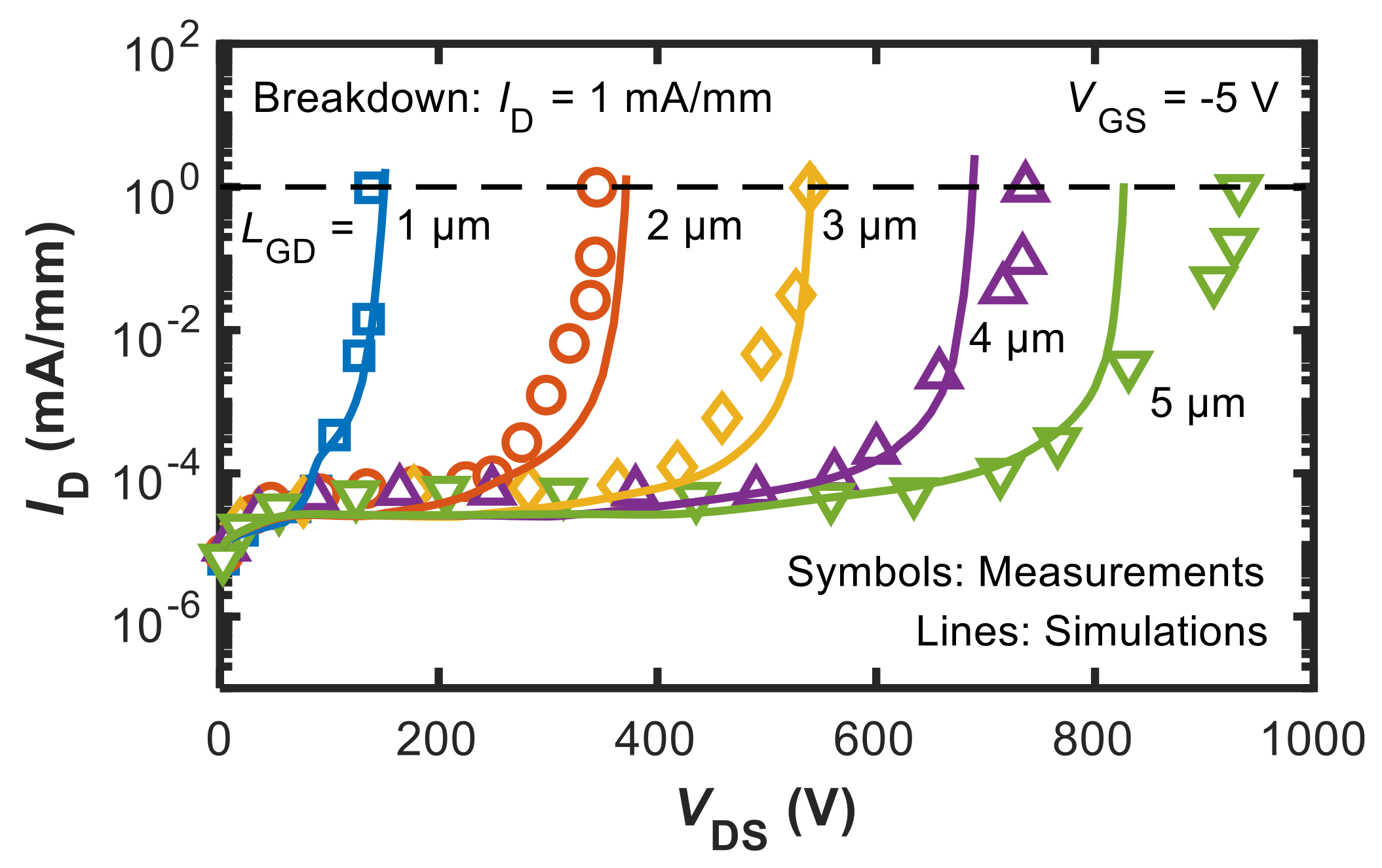
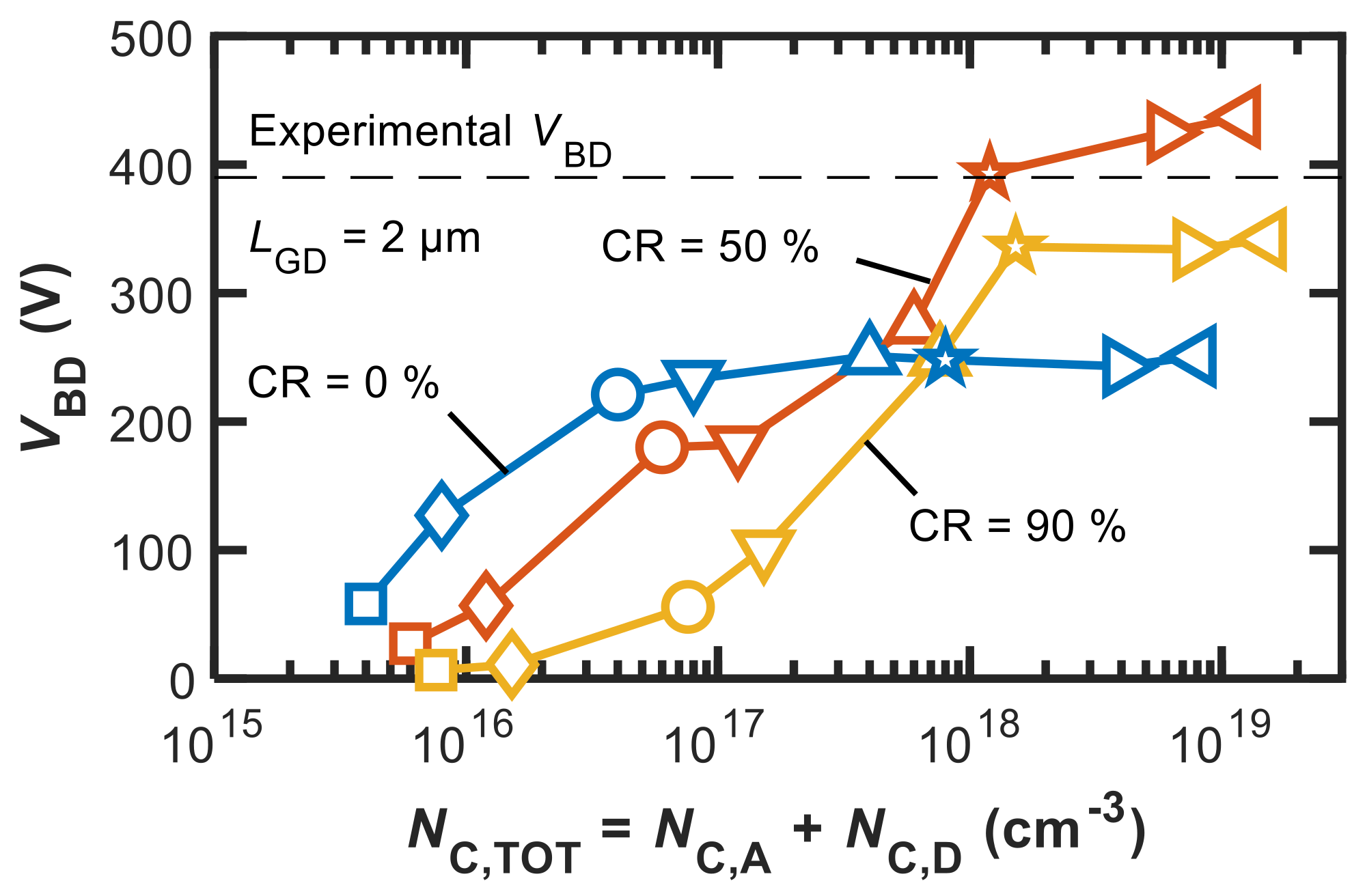
3.1. Breakdown Voltage

Figure 4 shows VBD as a function of NC,TOT for the different CR values. As can be noted, for all CR values, VBD first increases and then saturates with NC,TOT.
This behaviour is largely expected, as it is related to the decrease in the electric field peak at the gate edge resulting from the increase in the ionized acceptor density (negative charge). In essence, it is exactly to induce this effect that doping with acceptor impurities (like Fe and C) is adopted in power GaN HEMTs. The VBD saturation is attributable to the fact that once the electric-field peak moves from the gate edge to the drain contact, the beneficial effect of further increasing the acceptor concentration ceases.
In addition to confirming the above behaviour, Figure 4 provides us with two other pieces of information that are key to our purposes: (1) the maximum VBD attainable at large NC,TOT (VBD,max) is a non-monotonic function of CR, and (2) a significant CR value of about 50% must be assumed in order to obtain VBD in agreement with experiments. The reasons behind this can be understood with the aid of Figure 5 and Figure 6.
Figure 5 shows the lateral component of the electric field as a function of position along a cutline corresponding to the AlGaN/GaN interface at breakdown (VGS = −5 V, VDS = VBD) for NC,A = 8 × 1017 cm−3 in the three cases of CR = 0%, 50%, and 90%. As shown in Figure 5, increasing CR from 0% (i.e., NC,A = 8 × 1017 cm−3, ND,A = 0 cm−3) to 50% (i.e., NC,A = 8 × 1017 cm−3, ND,A = 4 × 1017 cm−3) and 90% (i.e., NC,A = 8 × 1017 cm−3, ND,A = 7.2 × 1017 cm−3) effectively modulates the electric field profile, relaxing the peak at the drain contact. Positively charged donors thus contribute to make the electric field profile more uniform (if the electric field peak has already moved to the drain contact). This explains why in Figure 4, VBD,max increases from about 250 V to about 450 V as CR is raised from 0% to 50%.
When further increasing CR to 90%, VBD,max is reduced. This behavior can be explained with the aid of Figure 6, which shows the modulus of the electron current density as a function of the device depth along a vertical cutline taken in the middle of the gate contact. As is clearly shown, the source–drain punch-through (or sub-threshold) current across the buffer increases as CR increases from 0% to 50% and 90%. This is a consequence of the higher NC,D that increases the conductivity of the buffer and thus reduces VBD.
In summary, without significant donor/acceptor compensation resulting in a CR of about 50%, it is not possible, according to our analysis, to explain the state-of-the-art VBD vs. LGD dependence with slopes of 150–200 V/mm [1,26,27,28], and, specifically in the case considered here, a VBD of about 370 V for a device with an LGD of 2 μm.

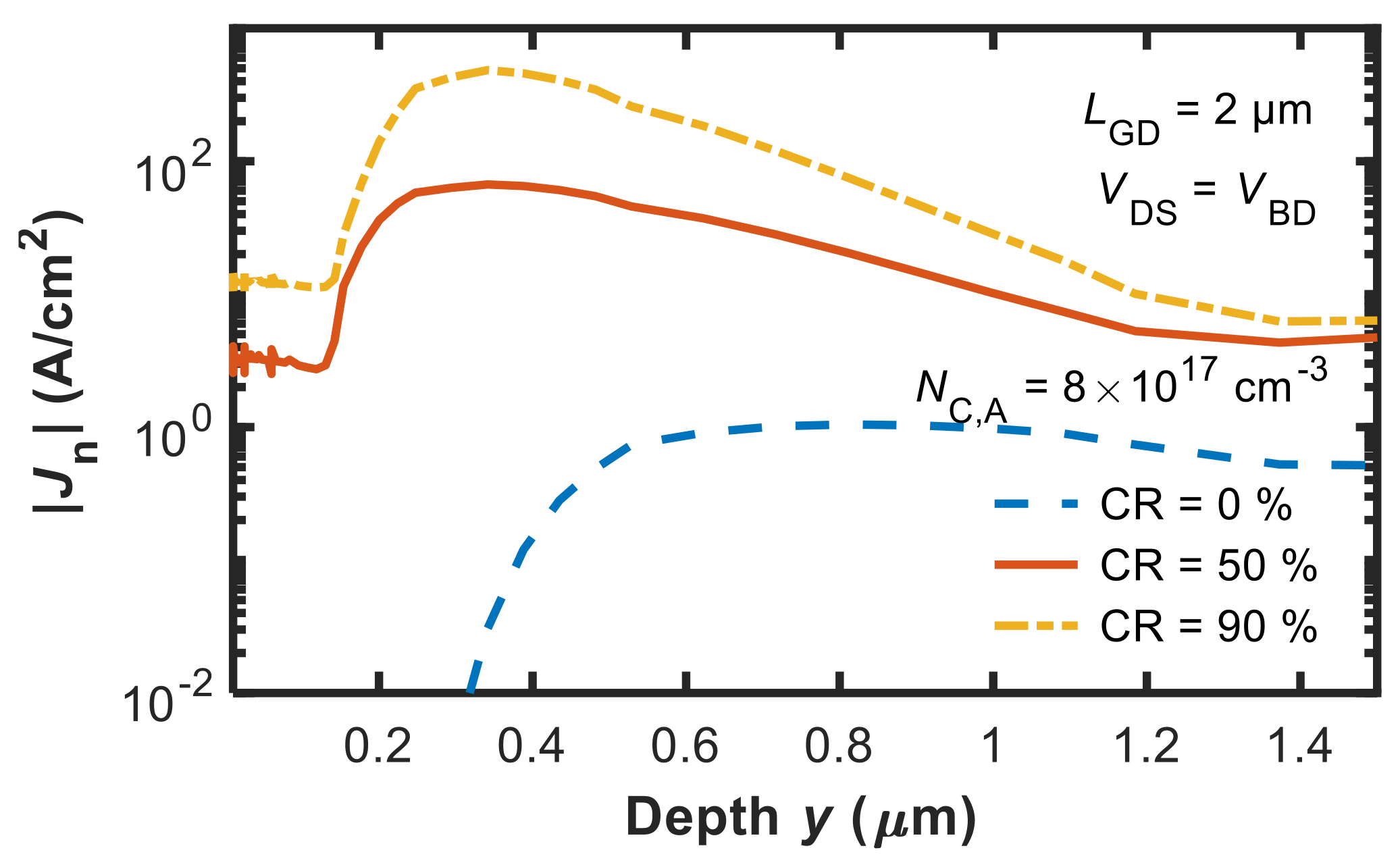
3.2. Current Collapse

The results of the sensitivity analysis on ΔICC are shown in Figure 7, where ΔICC is plotted against NC,EFF for the same CR values used for Figure 4. As it can be noted, ΔICC remains small (<10% in the specific devices considered here) regardless of CR when NC,EFF is smaller than 1017 cm−3. For higher NC,EFF, unless CR is very large (90% in our case), ΔICC increases steeply with NC,EFF, reaching values >60%, which are well above those reported for state-of-the-art C-doped GaN power HEMTs for NC,EFF values >1018 cm−3, the latter being instead quite typical for nominal C densities in extrinsically doped devices (i.e., using C precursors). In other words, according to this analysis it is unreasonable that C doping at high concentrations could simply translate to CN acceptors, as in this case DC-to-dynamic dispersion effects as current collapse and dynamic RON increase would make the device completely nonfunctional.
This is in agreement with previous results that showed how assuming CR = 0% (i.e., acceptors only) with concentrations on the order of the nominal C density (i.e., ~1018–1019 cm−3) resulted in large overestimation of current-collapse effects measured in actual devices of different technologies [4,12,18,29].

4. Discussion

By combining the results shown in Figure 4 and Figure 7, we observe that the VBD and ΔICC values measured in the device under study can be reproduced with a single set of parameters, and specifically, with the same NC,TOT and NC,EFF, only when considering a CR of about 50%. More generally, our results point to the necessity that a non-negligible part of incorporated C atoms results in donor-like levels or contribute to donor-like defect-impurity centers, thus compensating to a significant degree the dominant acceptor traps introduced by C doping.
The results presented in this work are relevant for the modeling of any GaN HEMT structure that incorporates C impurities (even unintentionally) in significant concentrations. High unintentional C doping concentrations can likely occur for metal-organic chemical vapor deposition (MOCVD)-grown, intentionally Fe-doped HEMTs for RF applications, where C incorporation comes as an inevitable consequence of the growth processing conditions [30].

5. Conclusions

We reported on the modeling of the compensation ratio (CR) between the donor and acceptor densities due to carbon doping in the buffer of lateral GaN power HEMTs to correctly simulate breakdown voltage (VBD) and current collapse (ΔICC). We showed that compensating shallow donor traps (NC,D) need to be considered in addition to the dominant deep acceptor traps (NC,A), in order to reproduce VBD and ΔICC with a single set of parameters. Furthermore, we identified that the primary dependence of VBDICC) on C doping is through the total (effective) concentration of acceptor and donor traps. The results presented here allow device engineers to properly model a given GaN HEMT technology that incorporates C in its structure (even unintentionally) by setting the CR value required to univocally reproduce both VBD and ΔICC data.

Author Contributions

Conceptualization, N.Z., A.C., and G.V.; formal analysis, N.Z., A.C., F.M.P., P.P., and G.V.; methodology, N.Z., A.C., and G.V.; writing—original draft preparation, N.Z., and G.V.; writing—review and editing, N.Z., A.C., F.M.P., P.P., and G.V.; supervision, A.C., F.M.P., P.P., and G.V. All authors have read and agreed to the published version of the manuscript.

Funding

This research received no external funding.

Conflicts of Interest

The authors declare no conflict of interest.

References

  1. Bahat-Treidel, E.; Brunner, F.; Hilt, O.; Cho, E.; Würfl, J.; Trankle, G. AlGaN/GaN/GaN:C back-barrier HFETs with breakdown voltage of over 1 kV and low RON× A. IEEE Trans. Electron. Devices 2010, 57, 3050–3058. [Google Scholar] [CrossRef]
  2. Uren, M.J.; Moreke, J.; Kuball, M. Buffer design to minimize current collapse in GaN/AlGaN HFETs. IEEE Trans. Electron. Devices 2012, 59, 3327–3333. [Google Scholar] [CrossRef] [Green Version]
  3. Del Alamo, J.A.; Lee, E.S. Stability and Reliability of Lateral GaN Power Field-Effect Transistors. IEEE Trans. Electron Devices 2019, 66, 4578–4590. [Google Scholar] [CrossRef]
  4. Chini, A.; Meneghesso, G.; Meneghini, M.; Fantini, F.; Verzellesi, G.; Patti, A.; Iucolano, F. Experimental and Numerical Analysis of Hole Emission Process from Carbon-Related Traps in GaN Buffer Layers. IEEE Trans. Electron. Devices 2016, 63, 3473–3478. [Google Scholar] [CrossRef]
  5. Remesh, N.; Mohan, N.; Raghavan, S.; Muralidharan, R.; Nath, D.N. Optimum Carbon Concentration in GaN-on-Silicon for Breakdown Enhancement in AlGaN/GaN HEMTs. IEEE Trans. Electron. Devices 2020, 67, 2311–2317. [Google Scholar] [CrossRef]
  6. Matsubara, M.; Bellotti, E. A first-principles study of carbon-related energy levels in GaN. I. Complexes formed by substitutional/interstitial carbons and gallium/nitrogen vacancies. J. Appl. Phys. 2017, 121, 195701. [Google Scholar] [CrossRef] [Green Version]
  7. Lyons, J.L.; Wickramaratne, D.; Van de Walle, C.G. A first-principles understanding of point defects and impurities in GaN. J. Appl. Phys. 2021, 129, 111101. [Google Scholar] [CrossRef]
  8. Lyons, J.L.; Janotti, A.; Van De Walle, C.G. Effects of carbon on the electrical and optical properties of InN, GaN, and AlN. Phys. Rev. B Condens. Matter Mater. Phys. 2014, 89, 1–8. [Google Scholar] [CrossRef]
  9. Rackauskas, B.; Uren, M.J.; Stoffels, S.; Zhao, M.; Decoutere, S.; Kuball, M. Determination of the self-compensation ratio of carbon in AlGaN for HEMTs. IEEE Trans. Electron. Devices 2018, 65, 1838–1842. [Google Scholar] [CrossRef] [Green Version]
  10. Uren, M.J.; Karboyan, S.; Chatterjee, I.; Pooth, A.; Moens, P.; Banerjee, A.; Kuball, M. “Leaky Dielectric” Model for the Suppression of Dynamic RON in Carbon-Doped AlGaN/GaN HEMTs. IEEE Trans. Electron. Devices 2017, 64, 2826–2834. [Google Scholar] [CrossRef] [Green Version]
  11. Koller, C.; Pobegen, G.; Ostermaier, C.; Pogany, D. Effect of Carbon Doping on Charging/Discharging Dynamics and Leakage Behavior of Carbon-Doped GaN. IEEE Trans. Electron. Devices 2018, 65, 5314–5321. [Google Scholar] [CrossRef]
  12. Verzellesi, G.; Morassi, L.; Meneghesso, G.; Meneghini, M.; Zanoni, E.; Pozzovivo, G.; Lavanga, S.; Detzel, T.; Häberlen, O.; Curatola, G. Influence of buffer carbon doping on pulse and AC behavior of insulated-gate field-plated power AlGaN/GaN HEMTs. IEEE Electron. Device Lett. 2014, 35, 443–445. [Google Scholar] [CrossRef]
  13. Joshi, V.; Tiwari, S.P.; Shrivastava, M. Part I: Physical Insight Into Carbon-Doping-Induced Delayed Avalanche Action in GaN Buffer in AlGaN/GaN HEMTs. IEEE Trans. Electron. Devices 2019, 66, 561–569. [Google Scholar] [CrossRef]
  14. Zagni, N.; Puglisi, F.M.; Pavan, P.; Chini, A.; Verzellesi, G. Insights into the off-state breakdown mechanisms in power GaN HEMTs. Microelectron. Reliab. 2019, 100–101, 113374. [Google Scholar] [CrossRef]
  15. Fariza, A.; Lesnik, A.; Bläsing, J.; Hoffmann, M.P.; Hörich, F.; Veit, P.; Witte, H.; Dadgar, A.; Strittmatter, A. On reduction of current leakage in GaN by carbon-doping. Appl. Phys. Lett. 2016, 109, 212102. [Google Scholar] [CrossRef]
  16. Zagni, N.; Chini, A.; Puglisi, F.M.; Meneghini, M.; Meneghesso, G.; Zanoni, E.; Pavan, P.; Verzellesi, G. “Hole Redistribution” Model Explaining the Thermally Activated RON Stress/Recovery Transients in Carbon-Doped AlGaN/GaN Power MIS-HEMTs. IEEE Trans. Electron. Devices 2021, 68, 697–703. [Google Scholar] [CrossRef]
  17. Zagni, N.; Chini, A.; Puglisi, F.M.; Pavan, P.; Verzellesi, G. The Role of Carbon Doping on Breakdown, Current Collapse, and Dynamic On-Resistance Recovery in AlGaN/GaN High Electron Mobility Transistors on Semi-Insulating SiC Substrates. Phys. Status Solidi 2019, 217, 1900762. [Google Scholar] [CrossRef]
  18. Meneghesso, G.; Silvestri, R.; Meneghini, M.; Cester, A.; Zanoni, E.; Verzellesi, G.; Pozzovivo, G.; Lavanga, S.; Detzel, T.; Haberlen, O.; et al. Threshold voltage instabilities in D-mode GaN HEMTs for power switching applications. In Proceedings of the IEEE International Reliability Physics Symposium (IRPS), Monterey, CA, USA, 14–18 April 2014; pp. 6–10. [Google Scholar] [CrossRef]
  19. Viey, A.G.; Vandendaele, W.; Jaud, M.-A.; Cluzel, J.; Barnes, J.-P.; Martin, S.; Krakovinsky, A.; Gwoziecki, R.; Plissonnier, M.; Gaillard, F.; et al. Investigation of nBTI degradation on GaN-on-Si E-mode MOSc-HEMT. In Proceedings of the IEEE International Electron Devices Meeting (IEDM), San Francisco, CA, USA, 7–11 December 2019; pp. 4.3.1–4.3.4. [Google Scholar] [CrossRef]
  20. Zagni, N.; Chini, A.; Puglisi, F.M.; Pavan, P.; Verzellesi, G. The effects of carbon on the bidirectional threshold voltage instabilities induced by negative gate bias stress in GaN MIS-HEMTs. J. Comput. Electron. 2020, 19, 1555–1563. [Google Scholar] [CrossRef]
  21. Zagni, N.; Cioni, M.; Chini, A.; Iucolano, F.; Puglisi, F.M.; Pavan, P.; Verzellesi, G. Mechanisms Underlying the Bidirectional V T Shift After Negative-Bias Temperature Instability Stress in Carbon-Doped Fully Recessed AlGaN/GaN MIS-HEMTs. IEEE Trans. Electron. Devices 2021, 68, 2564–2567. [Google Scholar] [CrossRef]
  22. Ber, E.; Osman, B.; Ritter, D. Measurement of the Variable Surface Charge Concentration in Gallium Nitride and Implications on Device Modeling and Physics. IEEE Trans. Electron. Devices 2019, 66, 2100–2105. [Google Scholar] [CrossRef] [Green Version]
  23. Bellotti, E.; Bertazzi, F. A numerical study of carrier impact ionization in Al xGa 1-xN. J. Appl. Phys. 2012, 111, 103711. [Google Scholar] [CrossRef]
  24. Armstrong, A.; Poblenz, C.; Green, D.S.; Mishra, U.K.; Speck, J.S.; Ringel, S.A. Impact of substrate temperature on the incorporation of carbon-related defects and mechanism for semi-insulating behavior in GaN grown by molecular beam epitaxy. Appl. Phys. Lett. 2006, 88, 1–4. [Google Scholar] [CrossRef]
  25. Joshi, V.; Tiwari, S.P.; Shrivastava, M. Part II: Proposals to Independently Engineer Donor and Acceptor Trap Concentrations in GaN Buffer for Ultrahigh Breakdown AlGaN/GaN HEMTs. IEEE Trans. Electron. Devices 2019, 66, 570–577. [Google Scholar] [CrossRef]
  26. Moens, P.; Liu, C.; Banerjee, A.; Vanmeerbeek, P.; Coppens, P.; Ziad, H.; Constant, A.; Li, Z.; De Vleeschouwer, H.; Roig-Guitart, J.; et al. An industrial process for 650 V rated GaN-on-Si power devices using in-situ SiN as a gate dielectric. In Proceedings of the IEEE International Symposium on Power Semiconductor Devices & IC’s (ISPSD), Waikoloa, HI, USA, 15–19 June 2014; pp. 374–377. [Google Scholar] [CrossRef]
  27. Cornigli, D.; Reggiani, S.; Gnani, E.; Gnudi, A.; Baccarani, G.; Moens, P.; Vanmeerbeek, P.; Banerjee, A.; Meneghesso, G. Numerical Investigation of the Lateral and Vertical Leakage Currents and Breakdown Regimes in GaN-on-Silicon Vertical Structures. In Proceedings of the IEEE International Electron Devices Meeting (IEDM), Washington, DC, USA, 7–9 December 2015; pp. 109–112, ISBN 9781467398947. [Google Scholar]
  28. Hilt, O.; Brunner, F.; Cho, E.; Knauer, A.; Bahat-Treidel, E.; Wurfl, J. Normally-off high-voltage p-GaN gate GaN HFET with carbon-doped buffer. In Proceedings of the IEEE International Symposium on Power Semiconductor Devices and ICs (ISPSD), Virtual, 30 May–3 June 2011; pp. 239–242. [Google Scholar] [CrossRef]
  29. Iucolano, F.; Parisi, A.; Reina, S.; Patti, A.; Coffa, S.; Meneghesso, G.; Verzellesi, G.; Fantini, F.; Chini, A. Correlation between dynamic Rdsou transients and Carbon related buffer traps in AlGaN/GaN HEMTs. In Proceedings of the IEEE International Reliability Physics Symposium (IRPS), Pasadena, CA, USA, 17–21 April 2016; pp. CD21–CD24. [Google Scholar] [CrossRef]
  30. Uren, M.J.; Kuball, M. Current collapse and kink effect in GaN RF HEMTs: The key role of the epitaxial buffer. In Proceedings of the IEEE BiCMOS and Compound Semiconductor Integrated Circuits and Technology Symposium (BCICTS), Monterey, CA, USA, 16–19 November 2020; pp. 1–8. [Google Scholar] [CrossRef]
Figure 1. Cross-section of the simulated Schottky-gate HEMT resembling the C-doped device in [1]. Dimensions are in μm (not to scale).
Micromachines 12 00709 g001
Figure 2. Calibrated simulations (lines) and measurements (symbols) of the off-state IDVDS curves. Measured data are taken from [1]. Adapted from [14].
Micromachines 12 00709 g002
Figure 3. Calibrated pulsed IDVDS curve simulations (lines) showing the achieved agreement in current-collapse measurements from [1] (symbols). Adapted from [17].
Micromachines 12 00709 g003
Figure 4. VBD vs. NC,TOT for CR = {0, 50, 90}%. The same symbols correspond to the same NC,A at different NC,D depending on CR.
Micromachines 12 00709 g004
Figure 5. Lateral component of the electric field (E) along the AlGaN/GaN interface at breakdown (VGS = −5 V, VDS = VBD) for CR = {0, 50, 90}% at the same NC,A value (8 × 1017 cm−3).
Micromachines 12 00709 g005
Figure 6. Modulus of the electron current density (|JN|) as a function of the device depth along a cutline taken in the middle of the gate contact for CR = {0, 50, 90}% at the same NC,A value (8 × 1017 cm−3).
Micromachines 12 00709 g006
Figure 7. ΔID,CC vs. NC,EFF for CR = {0, 50, 90}%. The same symbols correspond to the same NC,A at different NC,D depending on CR.
Micromachines 12 00709 g007
Table 1. List of main physical mechanisms, the respective models, and parameters used in the simulations.
Physical MechanismModelParametersValue
Impact IonizationChynoweth’s Lawa (electrons)2.32 × 106 cm−1
b (electrons)1.4 × 10⁷ V/cm
a (holes)5.41 × 106 cm−1
b (holes)1.89 × 10⁷ V/cm
Carbon Doping (Buffer)Acceptor Trap LevelConcentrationVariable
Energy Level0.9 + EV eV
Donor Trap LevelConcentrationVariable
Energy LevelEC—0.11 eV
Unintentional Doping (Channel)Donor Trap LevelConcentration1 × 1015 cm−3
Schottky Diode (Gate Contact)Thermionic and Field EmissionSchottky Barrier Height1 eV
Low-Field Mobility (GaN) µn1800 cm2/Vs
High-Field Saturation (GaN)Canali Modelvn,sat1.5 × 107 cm/s
Publisher’s Note: MDPI stays neutral with regard to jurisdictional claims in published maps and institutional affiliations.

