
Effects of Proton Irradiation on the Current Characteristics of SiN-Passivated AlGaN/GaN MIS-HEMTs Using a TMAH-Based Surface Pre-Treatment

 ,
,  and
and 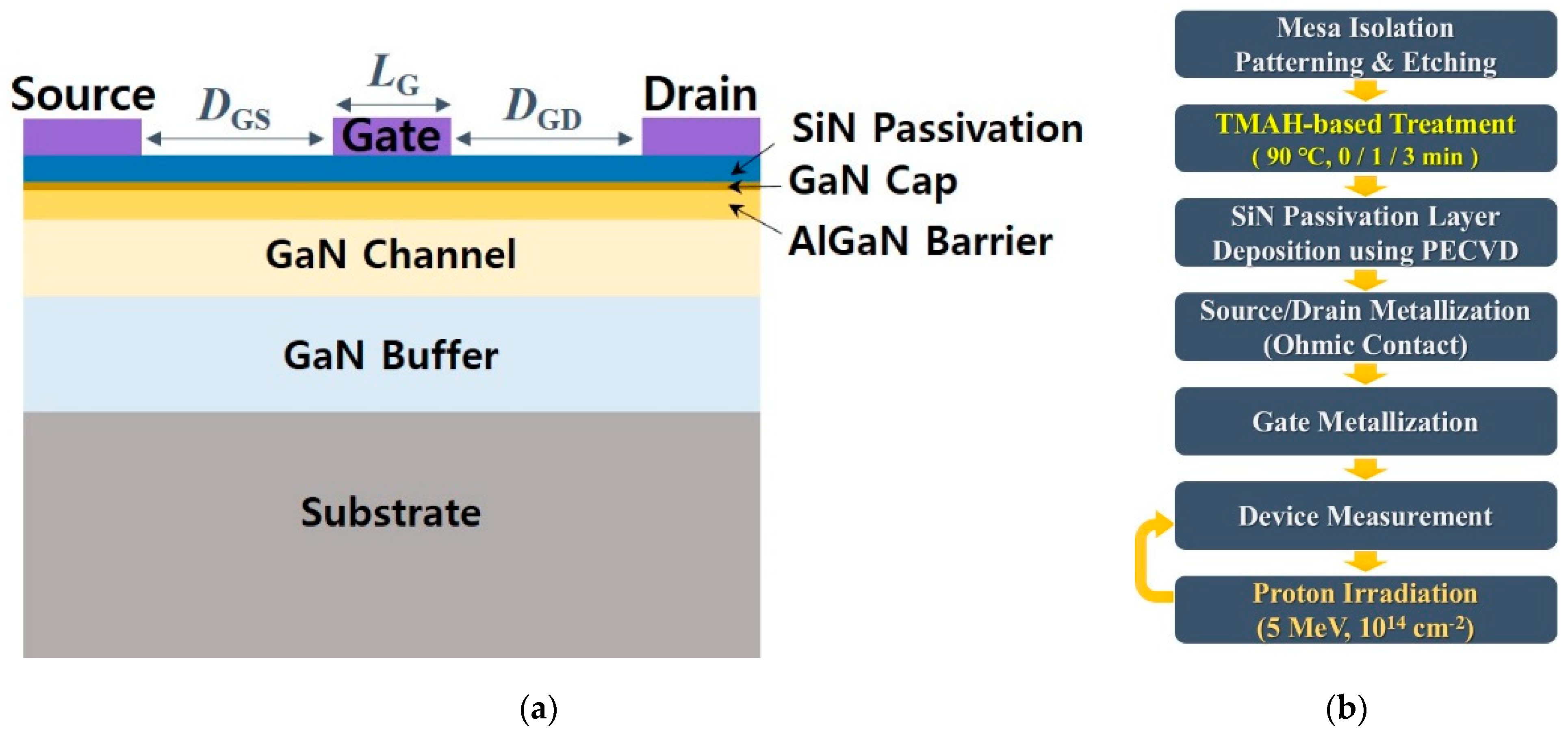
Abstract
:1. Introduction
2. Device Structure and Fabrication
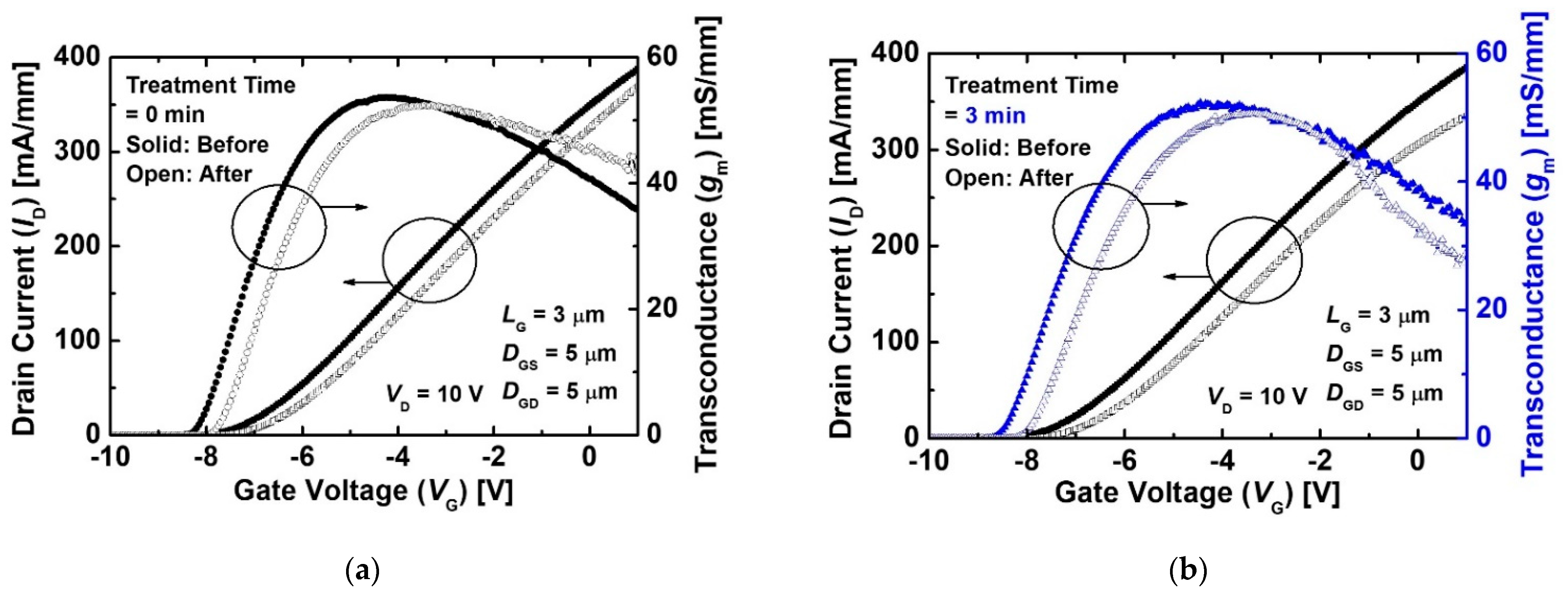
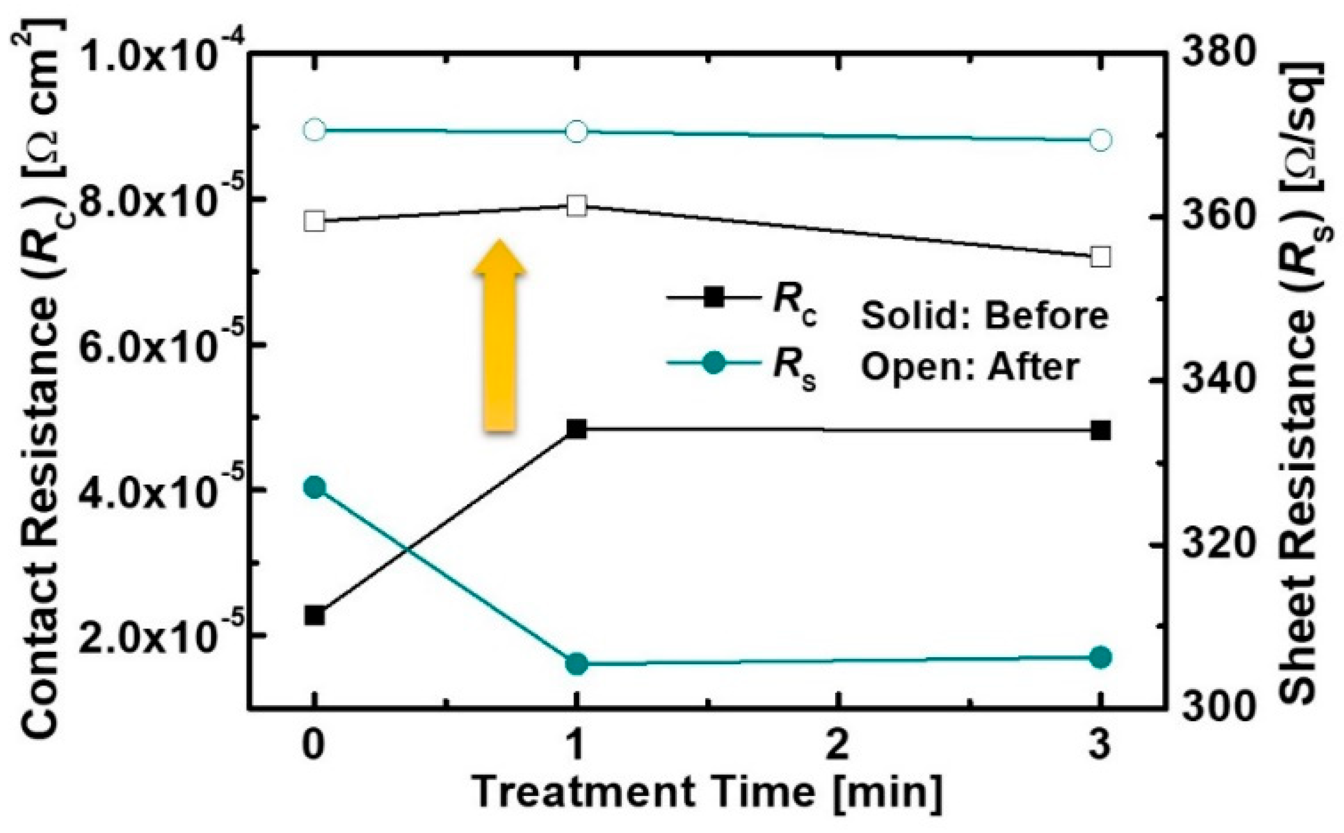
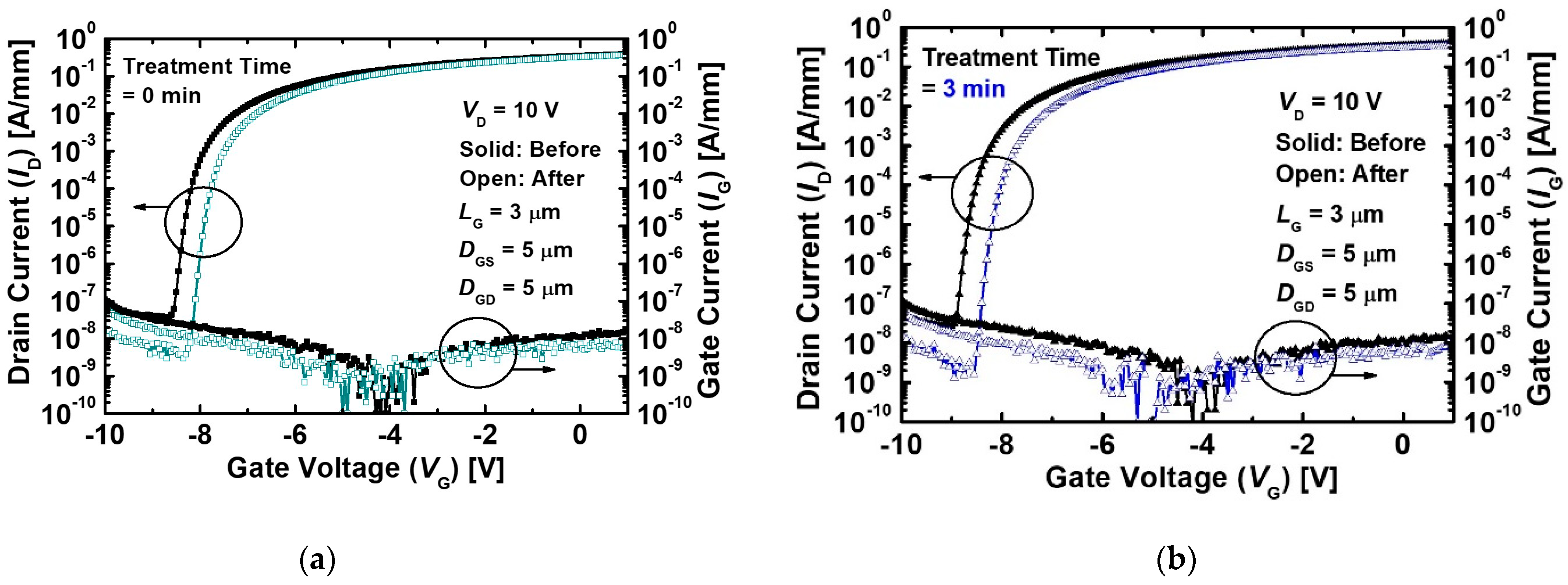
3. Results and Discussion
4. Conclusions
Author Contributions
Funding
Conflicts of Interest
References
- Mishra, U.K.; Parikh, P.; Wu, Y.-F. AlGaN/GaN HEMTs-an overview of device operation and applications. Proc. IEEE 2002, 90, 1022–1031. [Google Scholar] [CrossRef] [Green Version]
- Ikeda, N.; Niiyama, Y.; Kambayashi, H.; Sato, Y.; Nomura, T.; Kato, S.; Yoshida, S. GaN Power Transistors on Si Substrates for Switching Applications. Proc. IEEE 2010, 98, 1151–1161. [Google Scholar] [CrossRef]
- Baliga, B.J. Gallium nitride devices for power electronic applications. Semicond. Sci. Technol. 2013, 28, 074011. [Google Scholar]
- Ionascut-Nedelcescu, A.; Carlone, C.; Houdayer, A.; Bardeleben, H.J.; Cantin, J.-L.; Raymond, S. Radiation hardness of gallium nitride. IEEE Trans. Nucl. Sci. 2002, 49, 2733–2738. [Google Scholar] [CrossRef]
- Pearton, S.; Ren, F.; Patrick, E.; Law, M.E.; Polyakov, A.Y. Review—Ionizing Radiation Damage Effects on GaN Devices. ECS J. Solid State Sci. Technol. 2016, 5, Q35–Q60. [Google Scholar] [CrossRef] [Green Version]
- Weaver, B.D.; Anderson, T.J.; Koehler, A.D.; Greenlee, J.D.; Hite, J.; Shahin, D.I.; Kub, F.J.; Hobart, K.D. Editors’ Choice—On the Radiation Tolerance of AlGaN/GaN HEMTs. ECS J. Solid State Sci. Technol. 2016, 5, Q208–Q212. [Google Scholar] [CrossRef] [Green Version]
- Chang, S.-H.; Cho, K.J.; Jung, H.-W.; Kim, J.-J.; Jang, Y.-J.; Bae, S.-B.; Kim, D.-S.; Bae, Y.; Yoon, H.S.; Ahn, H.-K.; et al. Improvement of Proton Radiation Hardness Using ALD-Deposited Al2O3 Gate Insulator in GaN-Based MIS-HEMTs. ECS J. Solid State Sci. 2019, 8, Q245–Q248. [Google Scholar] [CrossRef]
- Lee, J.-H.; Kim, D.-S.; Kim, J.-G.; Ahn, W.-H.; Bae, Y.; Lee, J.-H. Effect of gate dielectrics on characteristics of high-energy proton-irradiated AlGaN/GaN MISHEMTs. Radiat. Phys. Chem. 2021, 184, 109473. [Google Scholar] [CrossRef]
- Fares, C.; Ren, F.; Pearton, S.; Yang, G.; Kim, J.; Lo, C.-F.; Johnson, J.W. Effect of proton irradiation energy on SiNx/AlGaN/GaN metal-insulator semiconductor high electron mobility transistors. J. Vac. Sci. Technol. B 2018, 36, 052202. [Google Scholar] [CrossRef]
- Gao, Z.; Romero, M.F.; Redondo-Cubero, A.; Pampillon, M.A.; Andres, E.S.; Calle, F. Effects of Gd2O3 Gate Dielectric on Proton-Irradiated AlGaN/GaN HEMTs. IEEE Electron Device Lett. 2017, 38, 611–614. [Google Scholar] [CrossRef]
- Luo, B.; Ren, F.; Allums, K.; Gila, B.; Onstine, A.; Abernathy, C.; Pearton, S.; Dwivedi, R.; Fogarty, T.; Wilkins, R.; et al. Proton irradiation of MgO- or Sc2O3 passivated AlGaN/GaN high electron mobility transistors. Solid State Electron. 2003, 47, 1015–1020. [Google Scholar] [CrossRef]
- Zhang, D.; Cheng, X.; Shen, L.; Zheng, L.; Gu, Z.; Zhou, W.; Liu, X.; Yu, Y. Influence of Poly-AlN Passivation on the Perfor-mance Improvement of 3-MeV Proton-Irradiated AlGaN/GaN MIS-HEMTs. IEEE Trans. Nucl. Sci. 2019, 66, 2215–2219. [Google Scholar] [CrossRef]
- He, J.; Feng, M.; Zhong, Y.; Wang, J.; Zhou, R.; Gao, H.; Zhou, Y.; Sun, Q.; Liu, J.; Huang, Y.; et al. On-wafer fabrication of cavity mirrors for InGaN-based laser diode grown on Si. Sci. Rep. 2018, 8, 7922. [Google Scholar] [CrossRef] [PubMed]
- Yoon, Y.J.; Seo, J.H.; Cho, M.S.; Kang, H.-S.; Won, C.-H.; Kang, I.M.; Lee, J.-H. TMAH-based wet surface pre-treatment for reduction of leakage current in AlGaN/GaN MIS-HEMTs. Solid State Electron. 2016, 124, 54–57. [Google Scholar] [CrossRef]
- Edwards, A.; Mittereder, J.; Binari, S.; Katzer, D.; Storm, D.; Roussos, J. Improved reliability of AlGaN-GaN HEMTs using an NH/sub 3/ plasma treatment prior to SiN passivation. IEEE Electron Device Lett. 2005, 26, 225–227. [Google Scholar] [CrossRef]
- Zaidi, Z.H.; Lee, K.B.; Guiney, I.; Qian, H.; Jiang, S.; Wallis, D.J.; Humphreys, C.J.; Houston, P.A. Sulfuric acid and hydro-gen peroxide surface passivation effects on AlGaN/GaN high electron mobility transistors. J. Appl. Phys. 2014, 116, 244501. [Google Scholar] [CrossRef]
- Romero, M.; Brana, A.; Cuerdo, R.; Jimenez, A.; Miguel-Sanchez, J.; Gonzalez-Posada, F.; Gomez, F.C.; Munoz, E. Effects of N2N2 Plasma Pretreatment on the SiN Passivation of AlGaN/GaN HEMT. IEEE Electron Device Lett. 2008, 29, 209–211. [Google Scholar] [CrossRef]
- Reddy, M.S.P.; Park, W.-S.; Im, K.-S.; Lee, J.-H. Dual-Surface Modification of AlGaN/GaN HEMTs Using TMAH and Piranha Solutions for Enhancing Current and 1/f-Noise Characteristics. IEEE J. Electron Devices Soc. 2018, 6, 791–796. [Google Scholar] [CrossRef]
- Kim, K.-W.; Jung, S.-D.; Kim, D.-S.; Kang, H.-S.; Im, K.-S.; Oh, J.-J.; Ha, J.-B.; Shin, J.-K.; Lee, J.-H. Effects of TMAH Treatment on Device Performance of Normally Off Al2O3/GaN MOSFET. IEEE Electron Device Lett. 2011, 32, 1376–1378. [Google Scholar] [CrossRef]
- Ziegler, J.F.; Ziegler, M.; Biersack, J. SRIM – The stopping and range of ions in matter (2010). Nucl. Instrum. Methods Phys. Res. Sect. B Beam Interact. Mater. Atoms 2010, 268, 1818–1823. [Google Scholar] [CrossRef] [Green Version]
- Polyakov, A.Y.; Pearton, S.; Frenzer, P.; Ren, F.; Liu, L.; Kim, J. Radiation effects in GaN materials and devices. J. Mater. Chem. C 2012, 1, 877–887. [Google Scholar] [CrossRef]
- Auret, F.D.; Goodman, S.A.; Koschnick, F.K.; Spaeth, J.-M.; Beaumont, B.; Gibart, P. Proton bombardment-induced electron traps in epitaxially grown n-GaN. Appl. Phys. Lett. 1999, 74, 407–409. [Google Scholar] [CrossRef]
- Liu, L.; Cuervo, C.V.; Xi, Y.; Ren, F.; Pearton, S.J.; Kim, H.-Y.; Kim, J.; Kravchenko, I.I. Impact of proton irradiation on dc performance of AlGaN/GaN high electron mobility transistors. J. Vac. Sci. Technol. B 2013, 31, 042202. [Google Scholar] [CrossRef]
- Cai, Y.; Zhou, Y.; Lau, K.M.; Chen, K.J. Control of Threshold Voltage of AlGaN/GaN HEMTs by Fluoride-Based Plasma Treatment: From Depletion Mode to Enhancement Mode. IEEE Trans. Electron Devices 2006, 53, 2207–2215. [Google Scholar] [CrossRef]
- Greenlee, J.D.; Specht, P.; Anderson, T.J.; Koehler, A.D.; Weaver, B.D.; Luysberg, M.; Dubon, O.D.; Kub, F.J.; Weatherford, T.R.; Hobart, K.D. Degradation mechanisms of 2 MeV proton irradiated AlGaN/GaN HEMTs. Appl. Phys. Lett. 2015, 107, 083504. [Google Scholar] [CrossRef] [Green Version]
- Kim, D.-S.; Lee, J.-H.; Kim, J.-G.; Yoon, Y.J.; Lee, J.S.; Lee, J.-H. Anomalous DC Characteristics of AlGaN/GaN HEMTs De-pending on Proton Irradiation Energies. ECS J. Solid State Sci. 2020, 9, 065005. [Google Scholar] [CrossRef]
- Lin, Y.-S.; Lain, Y.-W.; Hsu, S. AlGaN/GaN HEMTs with Low Leakage Current and High On/Off Current Ratio. IEEE Electron Device Lett. 2009, 31, 102–104. [Google Scholar] [CrossRef]
- Xu, Z.; Wu, W.; Ma, X.; Zhang, J.; Hao, Y.; Wang, J.; Cai, Y.; Liu, J.; Jin, C.; Yang, Z.; et al. Enhancement Mode (E-Mode) AlGaN/GaN MOSFET With 10−1310−13 A/mm Leakage Current and 10121012 ON/OFF Current Ratio. IEEE Electron Device Lett. 2014, 35, 1200–1202. [Google Scholar] [CrossRef]
- Liu, Z.H.; Ng, G.I.; Zhou, H.; Arulkumaran, S.; Maung, Y.K.T. Reduced surface leakage current and trapping effects in Al-GaN/GaN high electron mobility transistors on silicon with SiN/Al2O3 passivation. Appl. Phys. Lett. 2011, 98, 113506. [Google Scholar] [CrossRef]
- Wang, X.-D.; Hu, W.-D.; Chen, X.-S.; Lu, W. The Study of Self-Heating and Hot-Electron Effects for AlGaN/GaN Dou-ble-Channel HEMTs. IEEE Trans. Electron Devices 2012, 59, 1393–1401. [Google Scholar] [CrossRef]
- Ohi, K.; Asubar, J.; Nishiguchi, K.; Hashizume, T. Current Stability in Multi-Mesa-Channel AlGaN/GaN HEMTs. IEEE Trans. Electron Devices 2013, 60, 2997–3004. [Google Scholar] [CrossRef] [Green Version]
- Northrup, J.E.; Neugebauer, J. Strong affinity of hydrogen for the GaN(000-1) surface: Implications for molecular beam epitaxy and metalorganic chemical vapor deposition. Appl. Phys. Lett. 2004, 85, 3429–3431. [Google Scholar] [CrossRef]
- Wang, Y.-L.; Ren, F.; Zhang, U.; Sun, Q.; Yerino, C.D.; Ko, T.S.; Cho, Y.S.; Lee, I.H.; Han, J.; Pearton, S.J. Improved hydro-gen detection sensitivity in N-polar GaN Schottky diodes. Appl. Phys. Lett. 2009, 94, 212108. [Google Scholar] [CrossRef]
- Lelievre, J.-F.; Fourmond, E.; Kaminski, A.; Palais, O.; Ballutaud, D.; Lemiti, M. Study of the composition of hydrogenated silicon nitride SiNx:H for efficient surface and bulk passivation of silicon. Sol. Energy Mater. Sol. Cells 2009, 93, 1281–1289. [Google Scholar] [CrossRef] [Green Version]
- Vitanov, S.; Palankovski, V.; Maroldt, S.; Quay, R.; Murad, S.; Rodle, T.; Selberherr, S. Physics-Based Modeling of GaN HEMTs. IEEE Trans. Electron Devices 2012, 59, 685–693. [Google Scholar] [CrossRef]
- Chen, Z.; Yue, S.; Peng, C.; Zhang, Z.; Liu, C.; Wang, L.; Huang, Y.; Huang, Y.; He, Y.; Zhong, X.; et al. Hydrogen-Related Recovery Effect of AlGaN/GaN High-Electron-Mobility Transistors Irradiated by High-Fluence Protons. IEEE Trans. Nucl. Sci. 2021, 68, 118–123. [Google Scholar] [CrossRef]


Publisher’s Note: MDPI stays neutral with regard to jurisdictional claims in published maps and institutional affiliations. |
© 2021 by the authors. Licensee MDPI, Basel, Switzerland. This article is an open access article distributed under the terms and conditions of the Creative Commons Attribution (CC BY) license (https://creativecommons.org/licenses/by/4.0/).
Share and Cite
Yoon, Y.J.; Lee, J.S.; Suk, J.K.; Kang, I.M.; Lee, J.H.; Lee, E.J.; Kim, D.S. Effects of Proton Irradiation on the Current Characteristics of SiN-Passivated AlGaN/GaN MIS-HEMTs Using a TMAH-Based Surface Pre-Treatment. Micromachines 2021, 12, 864. https://0-doi-org.brum.beds.ac.uk/10.3390/mi12080864
Yoon YJ, Lee JS, Suk JK, Kang IM, Lee JH, Lee EJ, Kim DS. Effects of Proton Irradiation on the Current Characteristics of SiN-Passivated AlGaN/GaN MIS-HEMTs Using a TMAH-Based Surface Pre-Treatment. Micromachines. 2021; 12(8):864. https://0-doi-org.brum.beds.ac.uk/10.3390/mi12080864
Chicago/Turabian StyleYoon, Young Jun, Jae Sang Lee, Jae Kwon Suk, In Man Kang, Jung Hee Lee, Eun Je Lee, and Dong Seok Kim. 2021. "Effects of Proton Irradiation on the Current Characteristics of SiN-Passivated AlGaN/GaN MIS-HEMTs Using a TMAH-Based Surface Pre-Treatment" Micromachines 12, no. 8: 864. https://0-doi-org.brum.beds.ac.uk/10.3390/mi12080864