
Numerical Study of a Solar Cell to Achieve the Highest InGaN Power Conversion Efficiency for the Whole In-Content Range
 , , ,
, , ,
Abstract
:1. Introduction
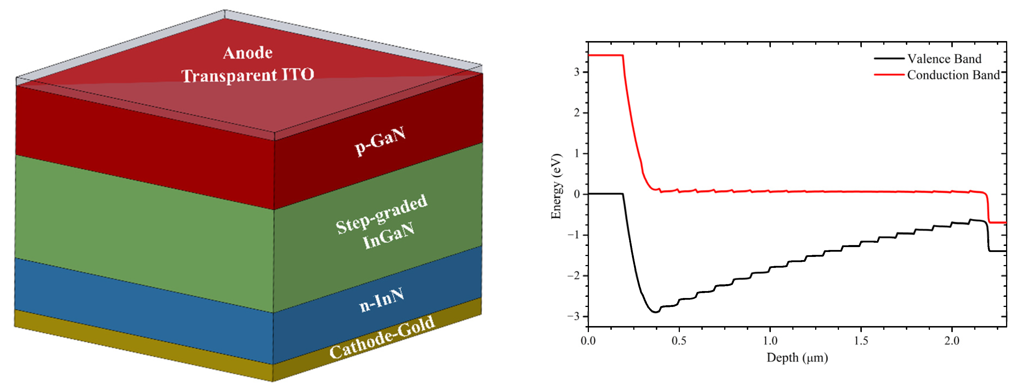
2. Materials and Methods
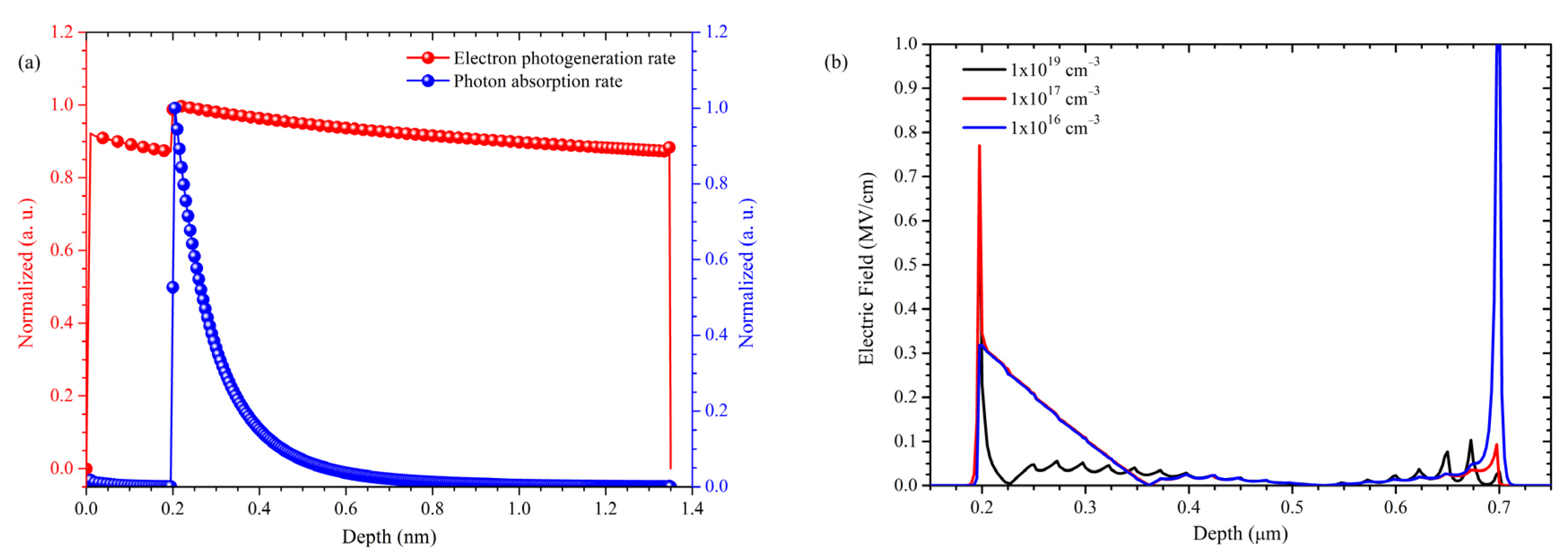
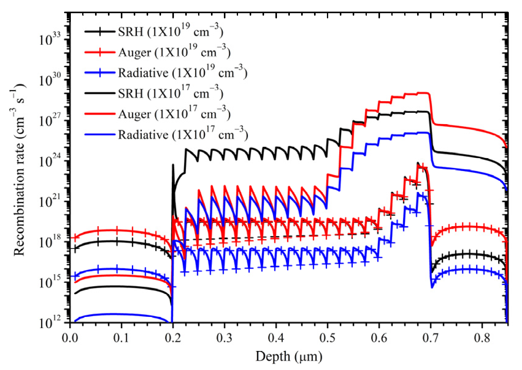
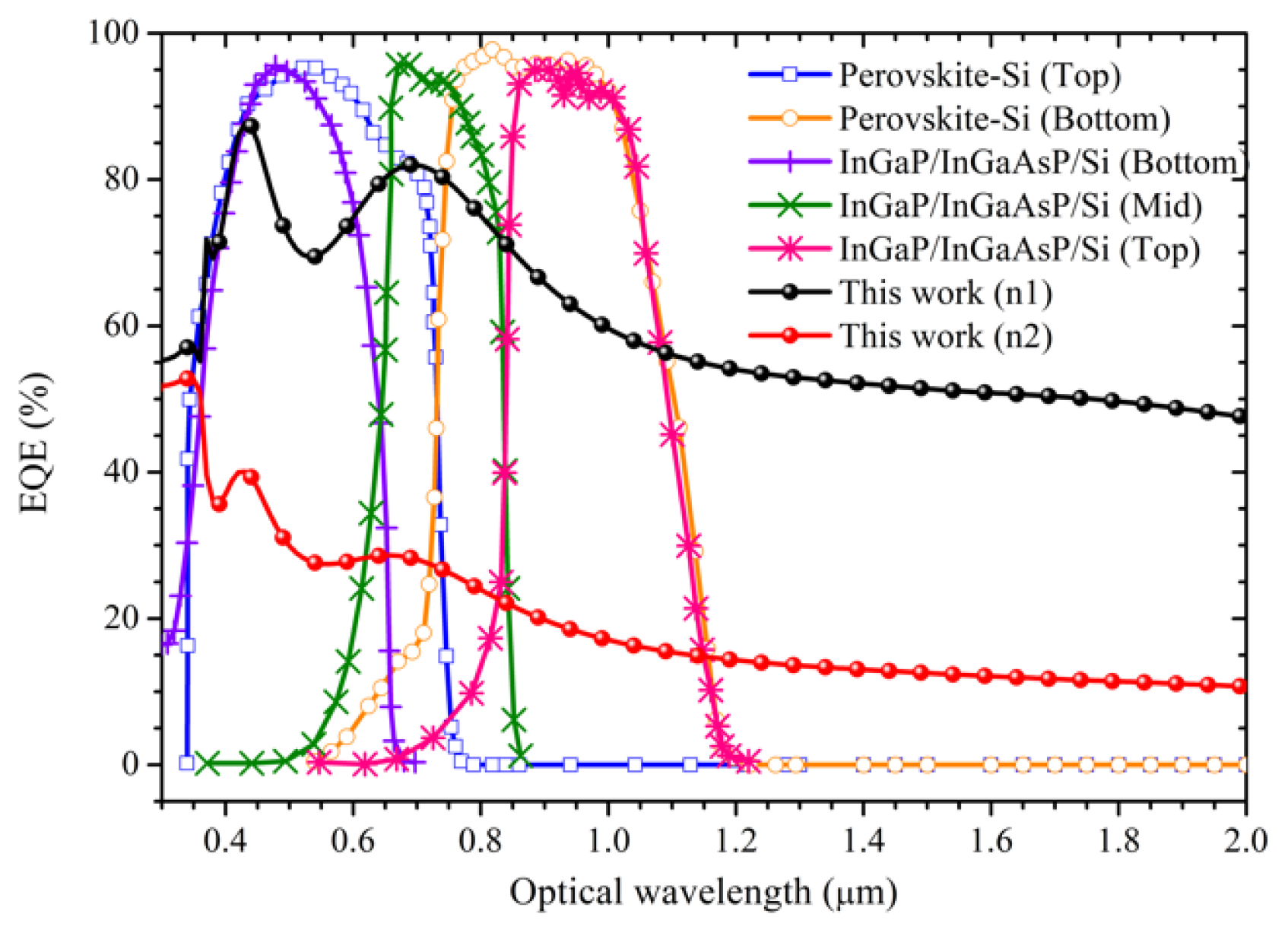
3. Results and Discussion
4. Conclusions
Author Contributions
Funding
Data Availability Statement
Acknowledgments
Conflicts of Interest
References
- Yoshikawa, K.; Kawasaki, H.; Yoshida, W.; Irie, T.; Konishi, K.; Nakano, K.; Uto, T.; Adachi, D.; Kanematsu, M.; Uzu, H.; et al. Silicon heterojunction solar cell with interdigitated back contacts for a photoconversion efficiency over 26%. Nat. Energy 2017, 2, 17032. [Google Scholar] [CrossRef]
- Bhuiyan, A.G.; Sugita, K.; Hashimoto, A.; Yamamoto, A. InGaN solar cells: Present state of the art and important challenges. IEEE J. Photovolt. 2012, 2, 276–293. [Google Scholar] [CrossRef]
- Valdueza-Felip, S.; Ajay, A.; Redaelli, L.; Chauvat, M.P.; Ruterana, P.; Cremel, T.; Jiménez-Rodríguez, M.; Kheng, K.; Monroy, E. P-i-n InGaN homojunctions (10–40% In) synthesized by plasma-assisted molecular beam epitaxy with extended photoresponse to 600nm. Sol. Energy Mater. Sol. Cells 2017, 160, 355–360. [Google Scholar] [CrossRef] [Green Version]
- Boudaoud, C.; Hamdoune, A.; Allam, Z. Simulation and optimization of a tandem solar cell based on InGaN. Math. Comput. Simul. 2020, 167, 194–201. [Google Scholar] [CrossRef]
- Islam, S.M.; Protasenko, V.; Rouvimov, S.; Xing, H.; Jena, D. High-quality InN films on GaN using graded InGaN buffers by MBE. Jpn. J. Appl. Phys. 2016, 55, 05FD12. [Google Scholar] [CrossRef] [Green Version]
- Bazioti, C.; Papadomanolaki, E.; Kehagias, T.; Walther, T.; Smalc-Koziorowska, J.; Pavlidou, E.; Komninou, P.; Karakostas, T.; Iliopoulos, E.; Dimitrakopulos, G.P. Defects, strain relaxation, and compositional grading in high indium content InGaN epilayers grown by molecular beam epitaxy. J. Appl. Phys. 2015, 118, 155301. [Google Scholar] [CrossRef] [Green Version]
- Pantzas, K.; El Gmili, Y.; Dickerson, J.; Gautier, S.; Largeau, L.; Mauguin, O.; Patriarche, G.; Suresh, S.; Moudakir, T.; Bishop, C.; et al. Semibulk InGaN: A novel approach for thick, single phase, epitaxial InGaN layers grown by MOVPE. J. Cryst. Growth 2013, 370, 57–62. [Google Scholar] [CrossRef]
- Hernández-Gutiérrez, C.A.; Morales-Acevedo, A.; Cardona, D.; Contreras-Puente, G.; López-López, M. Analysis of the performance of InxGa1−xN based solar cells. SN Appl. Sci. 2019, 1, 628. [Google Scholar] [CrossRef] [Green Version]
- Liliental-Weber, Z.; Yu, K.M.; Hawkridge, M.; Bedair, S.; Berman, A.E.; Emara, A.; Khanal, D.R.; Wu, J.; Domagala, J.; Bak-Misiuk, J. Structural perfection of InGaN layers and its relation to photoluminescence. Phys. Status Solidi Curr. Top. Solid State Phys. 2009, 6, 2626–2631. [Google Scholar] [CrossRef]
- Dagotto, E.; Hotta, T.; Moreo, A. Colossal magnetoresistant materials: The key role of phase separation. Phys. Rep. 2001, 344, 1–153. [Google Scholar] [CrossRef]
- Nagaev, É.L. Lanthanum manganites and other giant-magnetoresistance magnetic conductors. Uspekhi Fiz. Nauk 1996, 166, 857–858. [Google Scholar] [CrossRef]
- Khomskii, D. Phase separation, percolation and giant isotope effect in manganites. Phys. B Condens. Matter 2000, 280, 325–330. [Google Scholar] [CrossRef] [Green Version]
- Bagavath, C.; Kumar, J. Investigations on the structural, optical and electrical properties of InxGa1−xN thin films. Mater. Chem. Phys. 2019, 234, 318–322. [Google Scholar] [CrossRef]
- Rao, M.; Kim, D.; Mahajan, S. Compositional dependence of phase separation in InGaN layers. Appl. Phys. Lett. 2004, 85, 1961–1963. [Google Scholar] [CrossRef]
- Li, N.; Wang, S.-J.; Park, E.-H.; Feng, Z.C.; Tsai, H.-L.; Yang, J.-R.; Ferguson, I. Suppression of phase separation in InGaN layers grown on lattice-matched ZnO substrates. J. Cryst. Growth 2009, 311, 4628–4631. [Google Scholar] [CrossRef]
- Chen, Z.Z.; Qin, Z.X.; Hu, X.D.; Yu, T.J.; Yang, Z.J.; Tong, Y.Z.; Ding, X.M.; Zhang, G.Y. Study of photoluminescence and absorption in phase-separation InGaN films. Phys. B Condens. Matter 2004, 344, 292–296. [Google Scholar] [CrossRef]
- El Huni, W.; Karrakchou, S.; Halfaya, Y.; Arif, M.; Jordan, M.B.; Puybaret, R.; Ayari, T.; Ennakrachi, H.; Bishop, C.; Gautier, S.; et al. Nanopyramid-based absorber to boost the efficiency of InGaN solar cells. Sol. Energy 2019, 190, 93–103. [Google Scholar] [CrossRef]
- Gherasoiu, I.; Yu, K.M.; Reichertz, L.A.; Walukiewicz, W. InGaN doping for high carrier concentration in plasma-assisted molecular beam epitaxy. Phys. Status Solidi 2014, 11, 381–384. [Google Scholar] [CrossRef]
- Khettou, A.; Zeydi, I.; Chellali, M.; Ben Arbia, M.; Mansouri, S.; Helal, H.; Maaref, H. Simulation and optimization of InGaN Schottky solar cells to enhance the interface quality. Superlattices Microstruct. 2020, 142, 106539. [Google Scholar] [CrossRef]
- Wu, J.; Walukiewicz, W. Band gaps of InN and group III nitride alloys. Superlattices Microstruct. 2003, 34, 63–75. [Google Scholar] [CrossRef]
- Tangi, M.; De, A.; Shivaprasad, S.M. Role of dislocations and carrier concentration in limiting the electron mobility of InN films grown by plasma assisted molecular beam epitaxy. J. Appl. Phys. 2018, 123, 015701. [Google Scholar] [CrossRef]
- Ould Saad Hamady, S.; Adaine, A.; Fressengeas, N. Numerical simulation of InGaN Schottky solar cell. Mater. Sci. Semicond. Process. 2016, 41, 219–225. [Google Scholar] [CrossRef] [Green Version]
- Ma, N.; Wang, X.Q.; Liu, S.T.; Chen, G.; Pan, J.H.; Feng, L.; Xu, F.J.; Tang, N.; Shen, B. Hole mobility in wurtzite InN. Appl. Phys. Lett. 2011, 98, 18–21. [Google Scholar] [CrossRef]
- Ohnishi, K.; Amano, Y.; Fujimoto, N.; Nitta, S.; Watanabe, H.; Honda, Y.; Amano, H. Electrical properties and structural defects of p-type GaN layers grown by halide vapor phase epitaxy. J. Cryst. Growth 2021, 566–567, 126173. [Google Scholar] [CrossRef]
- Morkoç, H. General Properties of Nitrides. In Handbook of Nitride Semiconductors and Devices; Wiley Online Books: Hoboken, NJ, USA, 2008; pp. 1–129. [Google Scholar]
- Madi, L.; Bouchama, I.; Bouarissa, N. Effect of light wavelengths on the non-polar InGaN-based thin film solar cells performances using one-dimensional modeling. J. Sci. Adv. Mater. Devices 2019, 4, 509–514. [Google Scholar] [CrossRef]
- Tsai, Y.-C.; Bayram, C. Band Alignments of Ternary Wurtzite and Zincblende III-Nitrides Investigated by Hybrid Density Functional Theory. ACS Omega 2020, 5, 3917–3923. [Google Scholar] [CrossRef] [Green Version]
- Davydov, V.; Klochikhin, A.; Seisyan, R.; Emtsev, V.; Ivanov, S.; Bechstedt, F.; Furthmüller, J.; Harima, H.; Mudryi, A.; Aderhold, J.; et al. Absorption and Emission of Hexagonal InN. Evidence of Narrow Fundamental Band Gap. Phys. Status Solidi B. 2002, 80, r1–r3. [Google Scholar] [CrossRef]
- Tran, B.T.; Chang, E.Y.; Trinh, H.D.; Lee, C.T.; Sahoo, K.C.; Lin, K.L.; Huang, M.C.; Yu, H.W.; Luong, T.T.; Chung, C.C.; et al. Fabrication and characterization of n-In 0.4Ga 0.6N/p-Si solar cell. Sol. Energy Mater. Sol. Cells 2012, 102, 208–211. [Google Scholar] [CrossRef]
- Xing, Z.; Yang, W.; Yuan, Z.; Li, X.; Wu, Y.; Long, J.; Jin, S.; Zhao, Y.; Liu, T.; Bian, L.; et al. Growth and Characterization of High In-content InGaN grown by MBE using Metal Modulated Epitaxy Technique (MME). J. Cryst. Growth 2019, 516, 57–62. [Google Scholar] [CrossRef]
- Itoh, T.; Kobayashi, A.; Ueno, K.; Ohta, J.; Fujioka, H. Fabrication of InGaN thin-film transistors using pulsed sputtering deposition. Sci. Rep. 2016, 6, 29500. [Google Scholar] [CrossRef]
- Lin, S.K.; Wu, K.T.; Huang, C.P.; Liang, C.T.; Chang, Y.H.; Chen, Y.F.; Chang, P.H.; Chen, N.C.; Chang, C.A.; Peng, H.C.; et al. Electron transport in In-rich InxGa1−xN films. J. Appl. Phys. 2005, 97, 046101. [Google Scholar] [CrossRef]
- Yadav, B.S.; Mohanta, P.; Srinivasa, R.S.; Major, S.S. Electrical and optical properties of transparent conducting InxGa1−xN alloy films deposited by reactive co-sputtering of GaAs and Indium. Thin Solid Film. 2014, 555, 179–184. [Google Scholar] [CrossRef]
- Pantha, B.N.; Wang, H.; Khan, N.; Lin, J.Y.; Jiang, H.X. Origin of background electron concentration in InxGa1−xN alloys. Phys. Rev. B 2011, 84, 075327. [Google Scholar] [CrossRef] [Green Version]
- Hsu, L.; Jones, R.E.; Li, S.X.; Yu, K.M.; Walukiewicz, W. Electron mobility in InN and III-N alloys. J. Appl. Phys. 2007, 102, 73705. [Google Scholar] [CrossRef]
- Hu, Y.; Hernández-Gutiérrez, C.A.; Solís-Cisneros, H.I.; Santana, G.; Kudriatsev, Y.; Camas-Anzueto, J.L.; López-López, M. Blue luminescence origin and Mg acceptor saturation in highly doped zincblende GaN with Mg. J. Alloy. Compd. 2022, 897, 163133. [Google Scholar] [CrossRef]
- Wierer, J.J.; Fischer, A.J.; Koleske, D.D. The impact of piezoelectric polarization and nonradiative recombination on the performance of (0001) face GaN/InGaN photovoltaic devices. Appl. Phys. Lett. 2010, 96, 051107. [Google Scholar] [CrossRef]
- Chen, X.; Matthews, K.D.; Hao, D.; Schaff, W.J.; Eastman, L.F.; Walukiewicz, W.; Ager, J.W.; Yu, K.M. Characterization of Mg-doped InGaN and InAlN alloys grown by MBE for solar applications. In Proceedings of the 2008 33rd IEEE Photovoltaic Specialists Conference, San Diego, CA, USA, 11–16 May 2008; pp. 1–6. [Google Scholar]
- Pantha, B.N.; Sedhain, A.; Li, J.; Lin, J.Y.; Jiang, H.X. Electrical and optical properties of p-type InGaN. Appl. Phys. Lett. 2009, 95, 261904. [Google Scholar] [CrossRef] [Green Version]
- Kuo, D.H.; Tuan, T.T.A.; Li, C.C.; Yen, W.C. Electrical and structural properties of Mg-doped InxGa1−xN (x ≤ 0.1) and p-InGaN/n-GaN junction diode made all by RF reactive sputtering. Mater. Sci. Eng. B Solid-State Mater. Adv. Technol. 2015, 193, 13–19. [Google Scholar] [CrossRef]
- Sang, L.; Liao, M.; Ikeda, N.; Koide, Y.; Sumiya, M. Enhanced performance of InGaN solar cell by using a super-thin AlN interlayer. Appl. Phys. Lett. 2011, 99, 161109. [Google Scholar] [CrossRef]
- Kumakura, K.; Makimoto, T.; Kobayashi, N. High hole concentrations in Mg-doped InGaN grown by MOVPE. J. Cryst. Growth 2000, 221, 267–270. [Google Scholar] [CrossRef]
- Kumakura, K.; Makimoto, T.; Kobayashi, N. Activation Energy and Electrical Activity of Mg in Mg-doped InxGa1−xN (x < 0.2). Jpn. J. Appl. Phys 2000, 39, 337. [Google Scholar]
- Chen, P.C.; Chen, C.H.; Chang, S.J.; Su, Y.K.; Chang, P.C.; Huang, B.R. High hole concentration of p-type InGaN epitaxial layers grown by MOCVD. In Proceedings of the Thin Solid Films, Singapore, 14 August 2006; Volume 498, pp. 113–117. [Google Scholar]
- Sang, L.; Liao, M.; Koide, Y.; Sumiya, M. InGaN-based thin film solar cells: Epitaxy, structural design, and photovoltaic properties. J. Appl. Phys. 2015, 117, 105706. [Google Scholar] [CrossRef]
- Chang, C.A.; Tang, T.Y.; Chang, P.H.; Chen, N.C.; Liang, C. Te Magnesium doping of In-rich InGaN. Jpn. J. Appl. Phys. Part 1 Regul. Pap. Short Notes Rev. Pap. 2007, 46, 2840–2843. [Google Scholar] [CrossRef]
- Zhang, L.; Wang, R.; Liu, Z.; Cheng, Z.; Tong, X.; Xu, J.; Zhang, S.; Zhang, Y.; Chen, F. Regulation of hole concentration and mobility and first-principle analysis of mg-doping in InGaN grown by MOCVD. Materials 2021, 14, 5339. [Google Scholar] [CrossRef]
- Suski, T.; Staszczak, G.; Grzanka, S.; Czernecki, R.; Litwin-Staszewska, E.; Piotrzkowski, R.; Dmowski, L.H.; Khachapuridze, A.; Kryśko, M.; Perlin, P.; et al. Hole carrier concentration and photoluminescence in magnesium doped InGaN and GaN grown on sapphire and GaN misoriented substrates. J. Appl. Phys. 2010, 108, 023516. [Google Scholar] [CrossRef]
- Wang, X.; Che, S.B.; Ishitani, Y.; Yoshikawa, A. Hole mobility in Mg-doped p-type InN films. Appl. Phys. Lett. 2008, 92, 132108. [Google Scholar] [CrossRef]
- Wang, K.; Araki, T.; Yu, K.M.; Katsuki, T.; Mayer, M.A.; Alarcon-Llado, E.; Ager, J.W.; Walukiewicz, W.; Nanishi, Y. P-type InGaN across the entire alloy composition range. Appl. Phys. Lett. 2013, 102, 102111. [Google Scholar] [CrossRef]
- Jampana, B.R.; Ferguson, I.T.; Opila, R.L.; Honsberg, C.B. Utilizing polarization induced band bending for InGaN solar cell design. Mater. Res. Soc. Symp. Proc. 2009, 1167, 3–8. [Google Scholar] [CrossRef]
- Kumakura, K.; Makimoto, T.; Kobayashi, N. Mg-acceptor activation mechanism and transport characteristics in p-type InGaN grown by metalorganic vapor phase epitaxy. J. Appl. Phys. 2003, 93, 3370–3375. [Google Scholar] [CrossRef]
- Hernández-Gutiérrez, C.A.; Casallas-Moreno, Y.L.; Rangel-Kuoppa, V.-T.; Cardona, D.; Hu, Y.; Kudriatsev, Y.; Zambrano-Serrano, M.A.; Gallardo-Hernandez, S.; Lopez-Lopez, M. Study of the heavily p-type doping of cubic GaN with Mg. Sci. Rep. 2020, 10, 16858. [Google Scholar] [CrossRef]
- Tsai, Y.C.; Bayram, C. Mitigate self-compensation with high crystal symmetry: A first-principles study of formation and activation of impurities in GaN. Comput. Mater. Sci. 2021, 190, 110283. [Google Scholar] [CrossRef]
- Radojcic, R.; Hill, A.E.; Hampshire, M.J. A numerical model of a graded band gap CdSxTer1−x solar cell. Sol. Cells 1981, 4, 109–120. [Google Scholar] [CrossRef]
- Sassi, G. Theoretical analysis of solar cells based on graded bandgap structures. J. Appl. Phys. 1983, 54, 5421–5427. [Google Scholar] [CrossRef]
- Sarollahi, M.; Zamani, M.; Aldawsari, M.A.; Allaparthi, R.; Alhelais, R.; Refaei, M.A.; Uddin Maruf, M.H.; Ware, M.E. Modeling of Λ graded InxGa1−xN solar cells: Comparison of strained and relaxed features. J. Photonics Energy 2022, 12, 03510. [Google Scholar] [CrossRef]
- Morales-Acevedo, A. Effective absorption coefficient for graded bandgap semiconductors and the expected photocurrent density in solar cells. Sol. Energy Mater. Sol. Cells 2009, 93, 41–44. [Google Scholar] [CrossRef]
- Kazazis, S.A.; Papadomanolaki, E.; Androulidaki, M.; Kayambaki, M.; Iliopoulos, E. Optical properties of InGaN thin films in the entire composition range. J. Appl. Phys. 2018, 123, 125101. [Google Scholar] [CrossRef]
- Park, N.-G. Perovskite solar cells: An emerging photovoltaic technology. Mater. Today 2015, 18, 65–72. [Google Scholar] [CrossRef]
- Xu, Q.; Johnson, C.; Disney, C.; Pillai, S. Enhanced Broadband Light Trapping in c-Si Solar Cells Using Nanosphere-Embedded Metallic Grating Structure. IEEE J. Photovolt. 2016, 6, 61–67. [Google Scholar] [CrossRef]
- Kumawat, U.K.; Kumar, K.; Bhardwaj, P.; Dhawan, A. Indium-rich InGaN/GaN solar cells with improved performance due to plasmonic and dielectric nanogratings. Energy Sci. Eng. 2019, 7, 2469–2482. [Google Scholar] [CrossRef] [Green Version]
- Tsai, Y.-C.; Bayram, C.; Leburton, J.-P. Effect of Auger Electron–Hole Asymmetry on the Efficiency Droop in InGaN Quantum Well Light-Emitting Diodes. IEEE J. Quantum Electron. 2022, 58, 3300109. [Google Scholar] [CrossRef]
- Muyeed, S.A.A.; Borovac, D.; Xue, H.; Wei, X.; Song, R.; Tansu, N.; Wierer, J.J. Recombination Rates of InxGa1−xN/AlyGa1−yN/GaN Multiple Quantum Wells Emitting From 640 to 565 nm. IEEE J. Quantum Electron. 2021, 57, 3200207. [Google Scholar] [CrossRef]
- Green, M.A.; Dunlop, E.D.; Hohl-Ebinger, J.; Yoshita, M.; Kopidakis, N.; Hao, X. Solar Cell Efficiency Tables (Version 58). Prog. Photovolt. Res. Appl. 2021, 29, 657–667. [Google Scholar] [CrossRef]


| Parameter | InN | GaN |
|---|---|---|
| Bandgap | 0.7 eV [19,20] | 3.4 eV [13] |
| Electron mobility | 250 cm2/Vs [21] | 300 cm2/Vs [22] |
| Hole mobility | 30 cm2/Vs [23] | 14 cm2/Vs [24] |
| The effective mass of DOS in the CB | 0.11 [25] | 0.22 [25] |
| The effective mass of DOS in the VB | 1.63 [25] | 1.4 [25] |
| Dielectric constant | 15.3 [26] | 8.9 [22] |
| Parameter | Value |
|---|---|
| τp (electron lifetime) | 1.3 ns [62] |
| τp (hole lifetime) | 5.4 ns [62] |
| Auger recombination coefficients | 3.0 × 10⁻³⁰ cm6/s [63] |
| Radiative recombination coefficient | 1.4 × 10⁻¹³ cm3/s [64] |
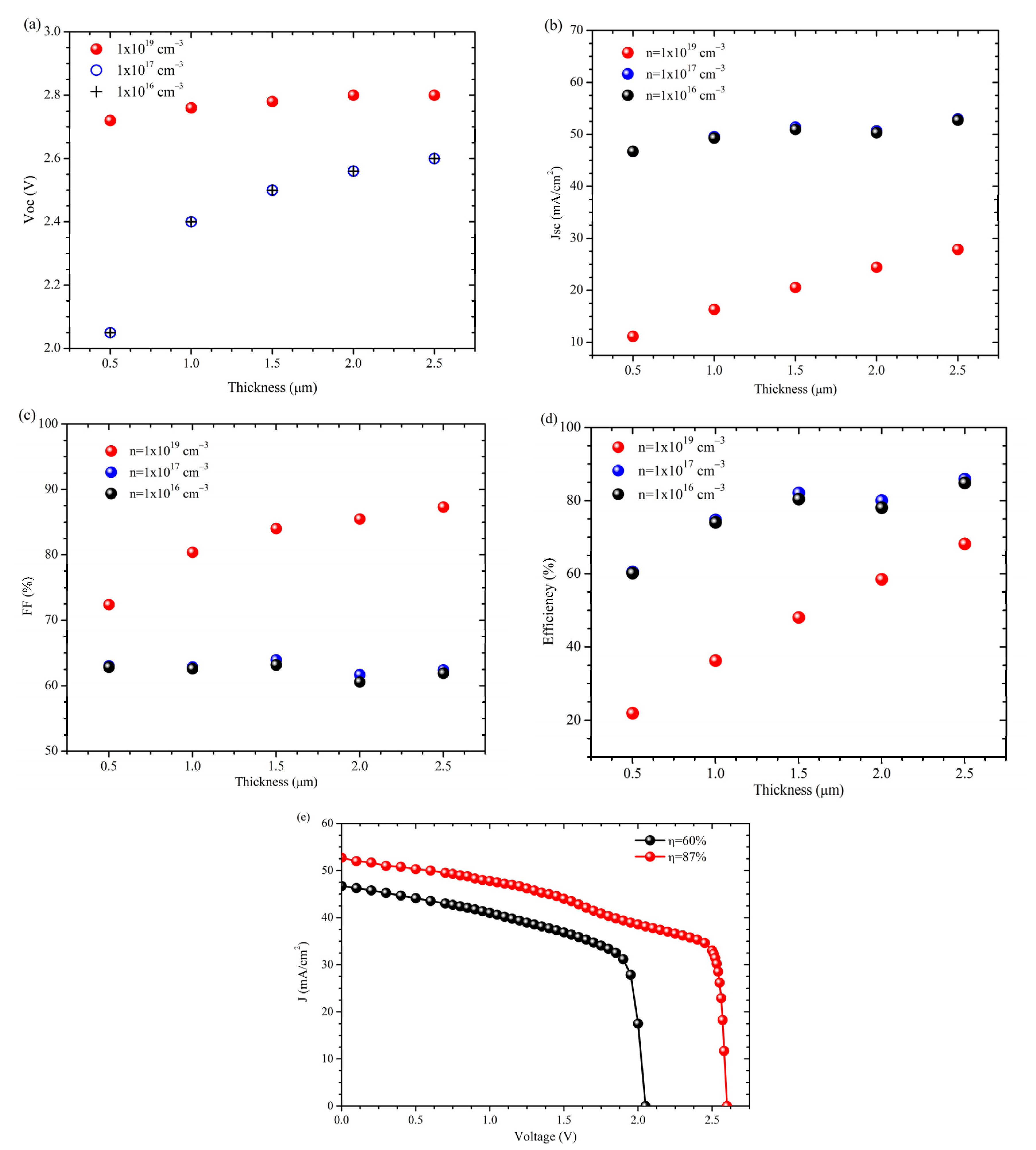
| Parameter | i = 1 × 1016 cm−3 | i = 1 × 1017 cm−3 | i = 1 × 1019 cm−3 | ||||||||||||
|---|---|---|---|---|---|---|---|---|---|---|---|---|---|---|---|
| Absorber Layer Thickness (µm) | Absorber Layer Thickness (µm) | Absorber Layer Thickness (µm) | |||||||||||||
| 0.5 | 1 | 1.5 | 2 | 2.5 | 0.5 | 1 | 1.5 | 2 | 2.5 | 0.5 | 1 | 1.5 | 2 | 2.5 | |
| VOC (V) | 2.05 | 2.40 | 2.50 | 2.56 | 2.60 | 2.05 | 2.40 | 2.50 | 2.56 | 2.60 | 2.71 | 2.76 | 2.78 | 2.80 | 2.80 |
| JSC (mA/cm2) | 46.72 | 49.28 | 50.93 | 50.32 | 52.72 | 46.72 | 49.57 | 51.40 | 50.66 | 52.95 | 11.15 | 16.35 | 20.57 | 24.44 | 27.89 |
| FF | 62.84 | 62.60 | 63.16 | 60.59 | 61.90 | 62.84 | 62.81 | 63.91 | 61.70 | 62.40 | 77.66 | 80.38 | 84.01 | 85.48 | 87.30 |
| Efficiency | 60.19 | 74.04 | 80.42 | 78.06 | 85.85 | 60.19 | 74.72 | 82.13 | 80.02 | 85.91 | 21.96 | 36.26 | 48.03 | 58.48 | 68.17 |
Publisher’s Note: MDPI stays neutral with regard to jurisdictional claims in published maps and institutional affiliations. |
© 2022 by the authors. Licensee MDPI, Basel, Switzerland. This article is an open access article distributed under the terms and conditions of the Creative Commons Attribution (CC BY) license (https://creativecommons.org/licenses/by/4.0/).
Share and Cite
Martínez-Revuelta, R.; Solís-Cisneros, H.I.; Trejo-Hernández, R.; Pérez-Patricio, M.; Paniagua-Chávez, M.L.; Grajales-Coutiño, R.; Camas-Anzueto, J.L.; Hernández-Gutiérrez, C.A. Numerical Study of a Solar Cell to Achieve the Highest InGaN Power Conversion Efficiency for the Whole In-Content Range. Micromachines 2022, 13, 1828. https://0-doi-org.brum.beds.ac.uk/10.3390/mi13111828
Martínez-Revuelta R, Solís-Cisneros HI, Trejo-Hernández R, Pérez-Patricio M, Paniagua-Chávez ML, Grajales-Coutiño R, Camas-Anzueto JL, Hernández-Gutiérrez CA. Numerical Study of a Solar Cell to Achieve the Highest InGaN Power Conversion Efficiency for the Whole In-Content Range. Micromachines. 2022; 13(11):1828. https://0-doi-org.brum.beds.ac.uk/10.3390/mi13111828
Chicago/Turabian StyleMartínez-Revuelta, Rubén, Horacio I. Solís-Cisneros, Raúl Trejo-Hernández, Madaín Pérez-Patricio, Martha L. Paniagua-Chávez, Rubén Grajales-Coutiño, Jorge L. Camas-Anzueto, and Carlos A. Hernández-Gutiérrez. 2022. "Numerical Study of a Solar Cell to Achieve the Highest InGaN Power Conversion Efficiency for the Whole In-Content Range" Micromachines 13, no. 11: 1828. https://0-doi-org.brum.beds.ac.uk/10.3390/mi13111828