
A Wideband High-Efficiency GaN MMIC Power Amplifier for Sub-6-GHz Applications
by
 , and
, and
Liulin Hu
1,2, 
Xuejie Liao
2,
Fan Zhang
2,
Haifeng Wu
2,
Shenglin Ma
3,
Qian Lin
4 and
and
Xiaohong Tang
1,* 1
School of Electronic Science and Engineering, University of Electronic Science and Technology of China, Chengdu 611731, China
2
Chengdu Ganide Technology Company, Ltd., Chengdu 610220, China
3
Department of Mechanical and Electrical Engineering, Xiamen University, Xiamen 361005, China
4
School of Physics and Electronic Information Engineering, Qinghai Minzu University, Xining 810007, China
*
Author to whom correspondence should be addressed.
Micromachines 2022, 13(5), 793; https://0-doi-org.brum.beds.ac.uk/10.3390/mi13050793
Submission received: 7 May 2022
/
Revised: 14 May 2022
/
Accepted: 17 May 2022
/
Published: 20 May 2022
(This article belongs to the Special Issue Wide Bandgap Based Devices: Design, Fabrication and Applications, Volume III)
Abstract
:The monolithic microwave integrated circuit (MMIC) power amplifiers serve an essential and critical role in RF transmit/receive (T/R) modules of phased array radar systems, mobile communication systems and satellite systems. Over recent years, there has been an increasing requirement to develop wideband high-efficiency MMIC high power amplifiers (HPAs) to accommodate wideband operation and reduce power consumption. This paper presents a wideband high efficiency MMIC HPA for Sub-6-GHz applications using a 0.25-μm gate-length D-mode GaN/SiC high electron mobility transistor (HEMT) process. The amplifier consists of two stages with two HEMT cells for the driver stage and eight HEMT cells for the power stage. To obtain a flat gain while maintaining the wideband characteristic, a gain equalization technique is employed in the inter-stage matching circuit. Meanwhile, a low-loss output matching network is utilized to ensure high efficiency. The fabricated HPA occupies a compact chip area of 14.35 mm2 including testing pads. Over the frequency range of 2–6 GHz, measured results of this HPA show a saturated continuous wave (CW) output power of 44.4–45.2 dBm, a power added efficiency (PAE) of 35.8–51.3%, a small signal gain of 24–25.5 dB, and maximum input and output return losses of 14.5 and 10 dB, respectively.
1. Introduction
Gallium nitride (GaN), as one of the wide band-gap semiconductors, features a high electric breakdown field and high electron saturation velocity. Compared to the gallium arsenide (GaAs) and silicon (CMOS or LDMOS) PAs [1,2,3,4], GaN PAs exhibit higher output power, higher efficiency, wider bandwidth and better thermal characteristics. Therefore, GaN technology is a good candidate for realizing high performance HPAs [5,6,7,8,9,10,11,12].
Over recent years, to meet the demand of wideband operation and low power consumption for sub-6-GHz applications, wideband high-efficiency HPAs have been greatly desired and studied. Several fabricated wideband GaN HPAs have been reported in [13,14,15,16,17,18,19,20] to cover the frequency range of 2–6 GHz while maintaining watt-level output power. A 2–6 GHz two-stage high-efficiency GaN MMIC power amplifier based on gain compensation structure was implemented in [13] to deliver an output power of 35 dBm with a PAE larger than 45%. However, this amplifier suffers from poor input matching networks. A wideband two-stage MMIC HPA was presented in [14], with an output power of 40 dBm and a relatively low PAE of 25%. In [15], a 0.5–6.5 GHz non-uniform distributed GaN power amplifier with a small chip area was presented to obtain an output power higher than 30 dBm and a PAE of 20–38.1%. In [20], a 2.5–10.5 GHz GaN power amplifier with distributed and reactively-matched amplifier stages was implemented to achieve a saturated output power of 18–37 W and PAE of 19–40%. Nevertheless, the amplifier exhibits degraded return losses and relatively large chip size. To date, it is still a challenge to design a 2–6 GHz GaN HPA that simultaneously features better than 10 dB input/output return losses, 20 watt output power and more than 35% PAE.
In this work, a wideband high-efficiency HPA for sub-6-GHz applications using a 0.25-μm gate-length GaN/SiC HEMT process at a nominal power supply voltage of 28 V is developed and measured. Measurements of this chip show competitive performance in terms of better than 14.5 dB/10 dB input/output return losses, a 44.4–45.2 dBm (27.5–33 Watt) output power, and a 35.8–51.3% PAE in comparison to previously reported HPAs.
The rest of this paper is organized as follows. The utilized GaN HEMT technology and its transistor characteristics will be first described. This is followed by the design and analysis of the proposed HPA. The measured performances of the fabricated amplifier will be given and discussed before conclusion.
2. GaN HEMT Technology and Characteristics
The two-stage PA is designed using a 0.25-μm gate-length D-mode GaN/SiC HEMT process on 100 μm SiC from WIN Semiconductors. The technology is suitable for high power applications from C-band through Ku-band. This process adopts a source-coupled field plate design to provide reliable operation breakdown voltage at high drain bias. Figure 1 demonstrates a representative transistor cross-section of the GaN HEMT process. The epitaxial layers were grown on top of the SiC wafer to constitute the HEMT and passive elements. The Au-metal layers consist of 0.6-μm MET0, 1.1-μm SFP, 1.1-μm MET1, and 4-μm MET2. The MET2 layer fulfills global interconnects to obtain low resistivity and high current handling capacity [21,22].
The HEMT of the GaN process features a cutoff frequency (fT) of 23 GHz and a maximum self-oscillation frequency (fmax) of 65 GHz. Typical DC characteristics of the transistor are breakdown voltage exceeding 100 V at Id = 1 mA/mm, and pinch-off voltage of −3.2 V, Idmax = 1.05 A/mm, Gmax = 340 mS/mm. The passive elements of the process include TaN thin film resistors with 50 Ω/square sheet resistivity, metal–insulator–metal (MIM) capacitors with capacitance density of 215 pF/mm2, round/square inductors, through-wafer vias for grounding, and air bridge crossover. The transistor and passive element models have been verified by measurements compared with simulations. Hence, the process design kit (PDK) models are accurate for our design in sub-6-GHz. The reliability information of the process can be referred to in [21].
The presented amplifier consists of two stages with two HEMT cells (6 × 150-μm GaN HEMT) for the driver stage and eight HEMT cells (6 × 200-μm GaN HEMT) for the power stage. For each HEMT cell of the power stage, Figure 2 shows its load pull contours of Pout, PAE and optimal load impedance at 2 and 6 GHz. The optimal load impedance of the transistor is chosen to approach the maximum PAE (>59.5%) while maintaining relatively large output power higher than 37.6 dBm at 6 GHz. It should be noted that the optimal load impedance is not constant across the frequency range of 2–6 GHz.
3. Power Amplifier Design
The motivation of this paper is to achieve a wideband high-efficiency MMIC PA with an output power of 44 dBm and a high PAE larger than 35% in the frequency range of 2–6 GHz. Figure 3 depicts the block diagram of the proposed two-stage PA. The total gate periphery is 11.4 mm from which the gate periphery ratios for the driver and power stages are equal to 3:16 to obtain sufficient driving power at the driver stage. The input matching and inter-stage matching circuits are designed to realize a good input match and a high gain with a good flatness, whilst the output matching circuit is selected to provide an optimal load match to obtain high efficiency and relatively large output power using the load/source pull simulation.
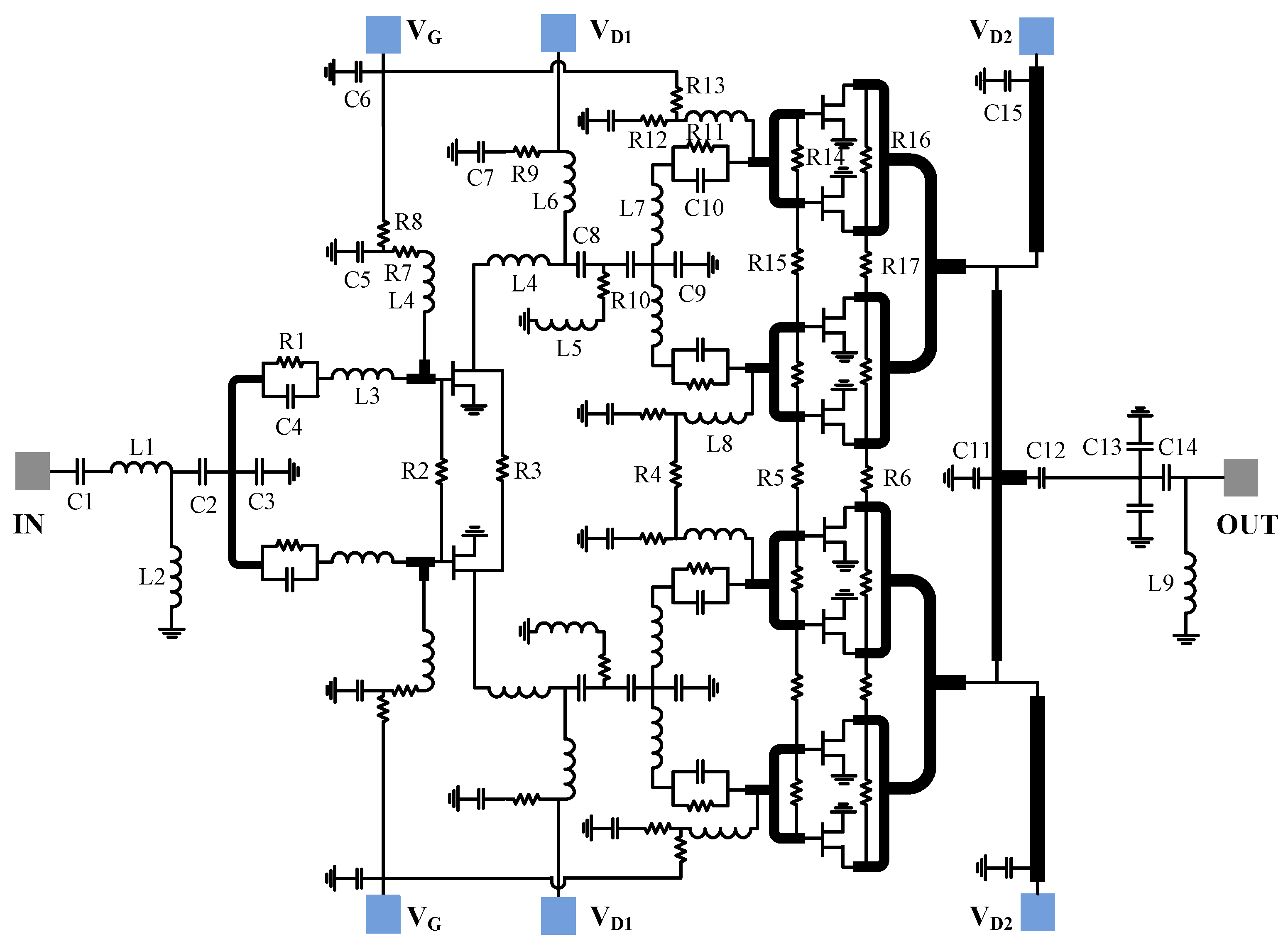
Figure 4 shows the circuit schematic of the designed amplifier in detail. The input matching, inter-stage matching and output matching circuits are realized by both lumped elements and distributed circuits. The parameter values of the relevant lumped elements are listed in Table 1. The gate of each transistor is connected with a parallel-combined resistor and capacitor to guarantee unconditional stability over the entire frequency range. The resistors placed between adjacent parallel transistors are utilized to avoid odd-mode oscillation. To gain wideband characteristics and flatness, a gain equalization technique is employed in the inter-stage matching circuit, since a low-loss output matching circuit is critical for gaining high efficiency [23,24]. To minimize insertion loss, the output matching circuit consists of low-loss double-layer microstrip lines, a shunt inductor, as well as series and shunt high-quality factor MIM capacitors. It should be mentioned that a series inductor is not adopted in the output matching due to its low-quality factor. Figure 5 gives the simulated insertion loss of the output matching network. It is seen that the loss of the output matching circuit is 0.86–0.65 dB across the frequency range of 2–6 GHz, ensuring high efficiency and high output power of the amplifier. It is worth mentioning that extensive lumped elements employed in the input and inter-stage matching circuits are benefical in limiting chip size.
The amplifier adopts a class-AB bias point with drain voltage of 28 V and gate voltage of −2.4 V to improve efficiency. The driver and power stages share the same gate voltage pads while containing individual drain voltage pads. Additionally, inductors are employed to feed the DC power supply of the driver stage as well as the gate of the power stage, and microstrip lines are chosen to feed the drain of the power stage due to the heavy current.
4. Power Amplifier Measurement Results
The two-stage HPA was implemented using a 0.25-μm gate-length D-mode GaN/SiC HEMT process. Figure 6 shows a microphotograph of the chip. Including testing pads, the chip occupies a die size of 3.5 mm × 4.1 mm with a SiC substrate thickness of 100 μm. To measure amplifier performance, the chip was mounted on a PCB board with bonding wires in a copper fixture as shown in Figure 7a. Each bonding wire is characterized with large inductance as a function of its length, and has small DC loss and capacitance. The amplifier was measured under CW conditions at the ambient temperature of 25 °C. The associated biased voltages are VG = −2.4 V, VD1 = 28 V, VD2 = 28 V, and a 1.2-A quiescent DC current is supplied. The test environment of the amplifier is demonstrated in Figure 7b.
The small-signal measurement of the HPA was completed via Keysight vector network analyzer (VNA) N5242 B (Keysight Technologies, Santa Rosa, CA, USA). Figure 8 demonstrates the measured S-parameters in comparison to the simulated ones. It is evident that the measurements and simulations are in good consistency. The amplifier achieves a small-signal gain of 24–25.5 dB with gain flatness less than ±0.75 dB across the frequency range of 2–6 GHz. The measured input and output return losses are better than 14.5 and 10 dB, respectively, achieving good input and output matching.
The large-signal measurement was measured using an Agilent signal generator N5182 B (Keysight Technologies, Santa Rosa, CA, USA), drive amplifier, attenuator, and Agilent power meter N1911 A under driving CW signal. The measured saturated output power (Pout), drain efficiency (DE), PAE, and gain against frequency are demonstrated in Figure 9. In this case, the input power (Pin) is fixed as 28 dBm. The output power varies from 44.4 to 45.2 dBm, the DE and PAE are within 36.4–52.7% and 35.8–51.3%, respectively, and the power gain is between 16.4–17.2 dB over the band of interest. Figure 10 shows the measured Pout, DE, PAE, and gain of the developed amplifier against input power at different frequencies. From 2 to 6 GHz, the Pout is 44.5–45 dBm with the associated DE greater than 36.7%, PAE higher than 35.7%, and power gain larger than 16.4 dB.
Table 2 summarizes the performance comparison between this work and state-of the-art HPAs. It is obvious that the presented wideband amplifier exhibits competitive performance in terms of input/output return loss, output power and efficiency compared to previously reported wideband counterparts.
5. Conclusions
This paper has reported the design and implementation of a wideband high-efficiency monolithic power amplifier suitable for sub-6-GHz applications utilizing a commercial 0.25-μm D-mode GaN HEMT process. The developed amplifier, with a compact chip area of 3.5 mm × 4.1 mm, demonstrates a delivered saturation output power of 44.4–45.2 dBm, a PAE higher than 35.8%, a small signal gain of 24–25.5 dB, and input and output return losses greater than 14.5 and 10 dB, respectively, over the entire 2–6 GHz bandwidth. It is believed that this outstanding MMIC power amplifier is promising and applicable for the T/R modules of sub-6-GHz systems due to its characteristics of wideband, good input/output match, high output power and high efficiency.
Author Contributions
Conceptualization, L.H. and X.T.; methodology, L.H., X.L. and H.W.; software, X.L., H.W. and Q.L.; validation, F.Z., X.L. and S.M.; formal analysis, L.H., F.Z. and H.W.; investigation, L.H., F.Z. and H.W.; resources, L.H., S.M. and Q.L.; data curation, H.W.; writing—original draft preparation, L.H. and F.Z.; writing—review and editing, X.T. and H.W.; visualization, F.Z.; supervision, X.T.; project administration, X.T.; funding acquisition, L.H., H.W. and X.T. All authors have read and agreed to the published version of the manuscript.
Funding
This research was funded by the National Natural Science Foundation, grant number 62161046, and the Natural Science Foundation of Qinghai Province, grant number 2021-ZJ-910.
Data Availability Statement
The presented data in this paper are available on request from the corresponding author.
Conflicts of Interest
The authors declare no conflict of interest.
References
- Ye, W.; Ma, K.; Yeo, K.S. 2.5 A 2 to 6 GHz Class-AB power amplifier with 28.4% PAE in 65 nm CMOS supporting 256 QAM. In Proceedings of the 2015 IEEE International Solid-State Circuits Conference-(ISSCC), San Francisco, CA, USA, 22–26 February 2015. [Google Scholar]
- Alizadeh, A.; Medi, A. Distributed class-J power amplifiers. IEEE Trans. Microw. Theory Tech. 2017, 65, 513–521. [Google Scholar] [CrossRef]
- Ding, X.; Zhang, L. A high-efficiency GaAs MMIC power amplifier for multi-standard system. IEEE Microw. Wirel. Compon. Lett. 2016, 26, 55–57. [Google Scholar] [CrossRef]
- Wu, H.F.; Lin, Q.; Chen, Y.J.; Hu, L.L.; Zhang, X.m.; Hu, D.H.; Chen, S.W. A 50 MHz to 6 GHz 1-Watt GaAs pHEMT stacked distributed power amplifier. In Proceedings of the 2019 IEEE MTT-S International Wireless Symposium (IWS), Guangzhou, China, 19–22 May 2019. [Google Scholar]
- Hookari, M.; Roshani, S.; Roshani, S. High-efficiency balanced power amplifier using miniaturized harmonics suppressed coupler. Int. J. RF Microw. Comput. Aided Eng. 2020, 30, e22252. [Google Scholar] [CrossRef]
- Sardin, D.; Reveyrand, T.; Popovic, Z. X-band 10 W MMIC high-gain power amplifier with up to 60% PAE. In Proceedings of the 2014 44th European Microwave Conference, Rome, Italy, 6–9 October 2014. [Google Scholar]
- Kong, K.S.; Nguyen, B.; Nayak, S.; Kao, M.Y. Ka-band MMIC high power amplifier (4 W at 30 GHz) with record compact size. In Proceedings of the IEEE Compound Semiconductor Integrated Circuit Symposium, Palm Springs, CA, USA, 30 October–2 November 2005. [Google Scholar]
- Aust, M.V.; Sharma, A.K.; Fordham, O.; Grundbacher, R.; To, R.; Tsai, R.S.; Lai, R. A 2.8-W Q-band high-efficiency power amplifier. IEEE J. Solid-State Circuits 2006, 41, 2241–2247. [Google Scholar] [CrossRef]
- Florian, C.; Cignani, R.; Santarelli, A.; Filicori, F. Design of 40-W ALGaN/GaN MMIC high power amplifiers for C-band SAR applications. IEEE Trans. Microw. Theory Tech. 2013, 61, 4492–4504. [Google Scholar] [CrossRef]
- Van Heijningen, M.; Hek, P.D.; Dourlens, C.; Fellon, P.; Adamiuk, G.; Ayllon, N.; Vliet, F.V. C-band single-chip radar front-end in AlGaN/GaN technology. IEEE Trans. Microw. Theory Tech. 2017, 65, 4428–4437. [Google Scholar] [CrossRef]
- Xie, H.; Cheng, Y.J.; Ding, Y.R.; Wang, L.; Fan, Y. A C-band high-efficiency power amplifier MMIC with second-harmonic control in 0.25 μm GaN HEMT Technology. IEEE Microw. Wirel. Compon. Lett. 2021, 31, 1303–1306. [Google Scholar] [CrossRef]
- Liu, R.J.; Zhu, X.W.; Xia, J.; Chen, P.; Yu, C.; Wu, X.L.; Chen, X. High efficiency wideband GaN MMIC Doherty power amplifier considering the output capacitor influence of the peaking transistor in class-C operation. IEEE Trans. Circuits Syst. I Reg. Pap. 2022, 69, 1932–1942. [Google Scholar] [CrossRef]
- Mao, S.M.; Liu, X.S.; Guo, Y.C.; Wu, Y.Q.; Xu, Y.H. A 2–6 GHz power amplifier with 45% PAE in 0.25 μm GaN technology. In Proceedings of the IEEE Asia-Pasific Microwave Conference, Singapore, 10–13 December 2019. [Google Scholar]
- Gonzalez-Garrido, M.A.; Grajal, J.; Cubilla, P.; Cetronio, A.; Lanzieri, C.; Uren, M. 2–6 GHz GaN MMIC Power Amplifiers for Electronic Warfare Applications. In Proceedings of the 2008 European Microwave Integrated Circuit Conference, Amsterdam, The Netherlands, 27–28 October 2008. [Google Scholar]
- Zhou, X.; Roy, L.; Amaya, R.E. 1 W, highly efficient, ultra broadband non-uniform distributed power amplifier in GaN. IEEE Microw. Wirel. Compon. Lett. 2013, 23, 208–210. [Google Scholar] [CrossRef]
- Qorvo. 2–6 GHz GaN Driver Amplifier. Available online: www.qorvo.com (accessed on 10 September 2019).
- Kim, D.W. An output matching technique for a GaN distributed power amplifier MMIC using tapered drain shunt capacitors. IEEE Microw. Wirel. Compon. Lett. 2015, 25, 603–605. [Google Scholar]
- Cree. CMPA2560025D, 25 W, 2.5–6 GHz, GaN MMIC, Power Amplifier. Available online: www.cree.com (accessed on 10 April 2020).
- Tang, B.W.; Lin, Z.K.; Xu, Y.H. A 2–6 GHz Single-chip Transceiver Front High-efficiency balanced power amplifier using miniaturized harmonics suppressed coupler. Int. J. RF Microw. Comput. Aided Eng. 2020, 30, e22252. [Google Scholar]
- Kamioka, J.; Hangai, M.; Komaru, R.; Morimoto, T.; Kamo, Y.; Shinjo, S. Over 20 W 2.5 to 10.5 GHz wideband two-stage GaN MMIC power amplifier with distributed and reactively-matched amplifier stages. In Proceedings of the 49th European Microwave Conference, Paris, France, 13 October 2019. [Google Scholar]
- Weng, M.H.; Lin, C.K.; Du, J.H.; Wang, W.C.; Wang, W.K.; Wohlmuth, W. Pure play GaN foundry 0.25 μm HEMT technology for RF applications. In Proceedings of the 2013 IEEE Compound Semiconductor Integrated Circuit Symposium (CSICS), Monterey, CA, USA, 13–19 October 2013. [Google Scholar]
- Wohlmuth, W.; Weng, M.H.; Lin, C.K.; Du, J.H.; Ho, S.Y.; Chou, T.Y.; Li, S.M.; Huang, C.; Wang, W.C.; Wang, W.K. AlGaN/GaN HEMT development targeted for X-band applications. In Proceedings of the IEEE Communications, Antennas and Electronics Systems (COMCAS), Tel Aviv, Israel, 21–23 October 2013. [Google Scholar]
- Kim, K.; Choi, H. High-efficiency high-voltage class F amplifier for high-frequency wireless ultrasound systems. PLoS ONE 2021, 16, e0249034. [Google Scholar] [CrossRef] [PubMed]
- Tao, H.Q.; Hong, W.; Zhang, B.; Yu, X.M. A compact 60 W X-Band GaN HEMT power amplifier MMIC. IEEE Microw. Wirel. Compon. Lett. 2017, 27, 73–75. [Google Scholar] [CrossRef]
Figure 1.
Schematic transistor cross-section of WIN Semiconductors’ 0.25μm GaN/SiC HEMT technology.

Figure 2.
Load-pull contours for Pout and PAE from 2 GHz to 6 GHz and ideal optimal load impedance.

Figure 3.
Functional block diagram of the presented sub-6-GHz MMIC HPA.

Figure 4.
Detailed circuit diagram of the sub-6-GHz HPA.

Figure 5.
Simulated insertion loss of the output matching network against frequency.

Figure 6.
Microphotograph of the fabricated chip.

Figure 7.
Photograph of the test fixture and small signal/large signal test environment of the HPA. (a) Test fixture; (b) test environment.
Figure 7.
Photograph of the test fixture and small signal/large signal test environment of the HPA. (a) Test fixture; (b) test environment.

Figure 8.
Simulated and measured S parameters.

Figure 9.
Measured saturated output power, DE, PAE and gain of the presented HPA against frequency with input fixed power of 28 dBm.
Figure 9.
Measured saturated output power, DE, PAE and gain of the presented HPA against frequency with input fixed power of 28 dBm.

Figure 10.
Large signal measured results of the presented HPA against input power at 2, 4 and 6 GHz. (a) Measured Pout and power gain against input power; (b) measured DE and PAE against input power.
Figure 10.
Large signal measured results of the presented HPA against input power at 2, 4 and 6 GHz. (a) Measured Pout and power gain against input power; (b) measured DE and PAE against input power.


Table 1.
Parameter values of the lumped elements of the proposed HPA.
| C1 | C2 | C3 | C4 | C5 | C6 | C7 | C8 | C9 | C10 | C11 |
| 4 pF | 3.8 pF | 1.5 pF | 1.5 pF | 2.3 pF | 9 pF | 35 pF | 1.8 pF | 0.2 pF | 3 pF | 1.1 pF |
| C12 | C13 | C14 | C15 | L1 | L2 | L3 | L4 | L5 | L6 | L7 |
| 2.2 pF | 2 pF | 2.2 pF | 35 pF | 1 nH | 2.2 nH | 1.3 nH | 1 nH | 3 nH | 1.2 nH | 1.5 nH |
| L8 | L9 | R1 | R2 | R3 | R4 | R5 | R6 | R7 | R8 | R9 |
| 2 nH | 2.2 nH | 35.6 Ω | 38 Ω | 19 Ω | 544 Ω | 38 Ω | 18 Ω | 76 Ω | 544 Ω | 50 Ω |
| R10 | R11 | R12 | R13 | R14 | R15 | R16 | R17 | |||
| 10 Ω | 20 Ω | 1.7 Ω | 544 Ω | 38 Ω | 38 Ω | 19 Ω | 19 Ω |
Table 2.
Comparison to previously published MMIC HPAs.
| Ref. | Process | Stage | Freq. (GHz) | S11/S22 (dB) | Pout (dBm) | PAE (%) | DC Supply (V) | Die Area (mm2) |
|---|---|---|---|---|---|---|---|---|
| [2] | GaAs | 1 | 1.5–10 | <−9.5/<−10 | 30.7 | 33–44 | 7 | 4.62 |
| [3] | GaAs | 2 | 2–6.5 | <−9.5/– | 31–32 | 31.4–51.5 | 5 | 9.62 |
| [4] | GaAs | 2 | 0.5–6 | <−13/<−15 | 29.5–31.1 | 22–29 | 12 | 4.8 |
| [12] | GaN | 1 | 4.6–5.5 | <−7+/– | 41.1–41.6 | 57.6–63.3 | 28 | 5.28 |
| [13] | GaN | 2 | 2–6 | <−2/<−8 | 35 | 45 | 25 | 3.52 |
| [14] | GaN | 2 | 2–6 | <−7/− | 40 | 25 | 25 | 23.04 |
| [15] | GaN | 1 | 0.5–6.5 | <−10/−7+ | 33.45 | 20–38.1 | 15 | 4 |
| [16] | GaN | 2 | 2–6 | <−20/<−5 | 31.5 | 31 | 25 | 3.21 |
| [17] | GaN | 1 | 2–6 | <−10/<−10 | 40.9–41.5 | 27–34 | 28 | 7.6 |
| [18] | GaN | 2 | 2.5–6 | <−6/<−5 | 44–45.7 | 30.7–32.8 | 28 | 16.82 |
| [19] | GaN | 2 | 2–6 | <−4/<−3 | 39 | 24–37 | 28 | – |
| [20] | GaN | 2 | 2.5–10.5 | <−5+/<−4.5+ | 42.5–45.7 | 19–40 | 40 | 20 |
| This work | GaN | 2 | 2–6 | <−14.5/<−10 | 44.4–45.2 | 35.8–51.3 | 28 | 14.35 |
Freq.: frequency; +: estimated value from figure.
Publisher’s Note: MDPI stays neutral with regard to jurisdictional claims in published maps and institutional affiliations. |
© 2022 by the authors. Licensee MDPI, Basel, Switzerland. This article is an open access article distributed under the terms and conditions of the Creative Commons Attribution (CC BY) license (https://creativecommons.org/licenses/by/4.0/).
Share and Cite
MDPI and ACS Style
Hu, L.; Liao, X.; Zhang, F.; Wu, H.; Ma, S.; Lin, Q.; Tang, X. A Wideband High-Efficiency GaN MMIC Power Amplifier for Sub-6-GHz Applications. Micromachines 2022, 13, 793. https://0-doi-org.brum.beds.ac.uk/10.3390/mi13050793
AMA Style
Hu L, Liao X, Zhang F, Wu H, Ma S, Lin Q, Tang X. A Wideband High-Efficiency GaN MMIC Power Amplifier for Sub-6-GHz Applications. Micromachines. 2022; 13(5):793. https://0-doi-org.brum.beds.ac.uk/10.3390/mi13050793
Chicago/Turabian StyleHu, Liulin, Xuejie Liao, Fan Zhang, Haifeng Wu, Shenglin Ma, Qian Lin, and Xiaohong Tang. 2022. "A Wideband High-Efficiency GaN MMIC Power Amplifier for Sub-6-GHz Applications" Micromachines 13, no. 5: 793. https://0-doi-org.brum.beds.ac.uk/10.3390/mi13050793
Note that from the first issue of 2016, this journal uses article numbers instead of page numbers. See further details here.