


Design of the Threshold-Controllable Memristor Emulator Based on NDR Characteristics

School of Electronics and Information, Hangzhou Dianzi University, Hangzhou 310018, China
*
Author to whom correspondence should be addressed.
Micromachines 2022, 13(6), 829; https://0-doi-org.brum.beds.ac.uk/10.3390/mi13060829
Submission received: 13 April 2022
/
Revised: 20 May 2022
/
Accepted: 24 May 2022
/
Published: 26 May 2022
(This article belongs to the Special Issue Novel Computing Architectures and Digital Circuit Designs Using Memristors and Memristive Systems)
Abstract
:Due to the high manufacturing cost of memristors, an equivalent emulator has been employed as one of the mainstream approaches of memristor research. A threshold-type memristor emulator based on negative differential resistance (NDR) characteristics is proposed, with the core part being the R-HBT network composed of transistors. The advantage of the NDR-based memristor emulator is the controllable threshold, where the state of the memristor can be changed by setting the control voltage, which makes the memristor circuit design more flexible. The operation frequency of the memristor emulator is about 250 kHz. The experimental results prove the feasibility and correctness of the threshold-controllable memristor emulator circuit.
1. Introduction
Memristors have received widespread attention in the world since HP Labs successfully manufactured TiO2 memristors in 2008 [1,2]. A memristor is a non-linear resistor with memory characteristics, and its i-v characteristic curve is related to the frequency. Its proven good performance implies significant potential in the fields of chaotic circuits [3,4,5], non-volatile memory [6,7], digital logic [8,9], artificial neural networks [10,11,12], and non-linear circuits. In general, the research of memristors includes physical implementation [2,13,14], applications in electronic circuits [15,16], and memristor emulators [17,18,19,20,21,22,23,24,25,26].
The studies on memristor emulators have achieved many results, and a variety of different memristor emulator circuit structures have been proposed, which can be divided into two categories: grounded memristor emulator circuits [18,19] and floating memristor emulator circuits [20,21,22,23,24,25,26]. To design a grounded memristor emulator is easier than a floating memristor emulator. However, due to the fact that one terminal is grounded, the grounded memristor emulator has limited features in circuit designs and applications, and is not suitable for use as a two-terminal device in more complicated circuits [20]. Compared with grounded memristor emulators, the application of floating memristor emulators is more flexible, which can be realized by various active elements, such as second-generation current conveyor (CCII) [21], operational transconductance amplifier (OTA) [22], multi outputs OTA [23], current voltage differencing transconductance amplifier (VDTA) [24], and voltage differencing current conveyor (VDCC) [25] with accompanying passive elements and possibly analog multipliers (AD633) [26]. Although some commercial memristor chips are already available on the market, e.g., Knowm.com (accessed on 9 May 2019) [27], memristor emulators have yet to be widely studied and adopted due to their lower cost.
This article proposes a novel floating threshold-type memristor emulator devised based on the negative differential resistance (NDR) characteristic. Not only does the proposed memristor emulator have a high operating frequency, but it also possesses the controllable threshold voltage, an attribute that makes it more suited for digital logic circuit applications.
The rest of this paper is organized as follows: in Section 2, the NDR hysteresis unit is introduced and improved on the basis of the R-HBT-NDR unit, and its simulation and hardware experiments are carried out. Section 3 presents the circuit diagram of the threshold-controllable memristor based on NDR characteristics. Section 4 provides the specific circuit implementation and the detailed analysis of its operating principle. In Section 5, the simulation experimental results are presented. Section 6 summarizes the paper.
2. Improvement and Design of NDR Hysteresis Unit
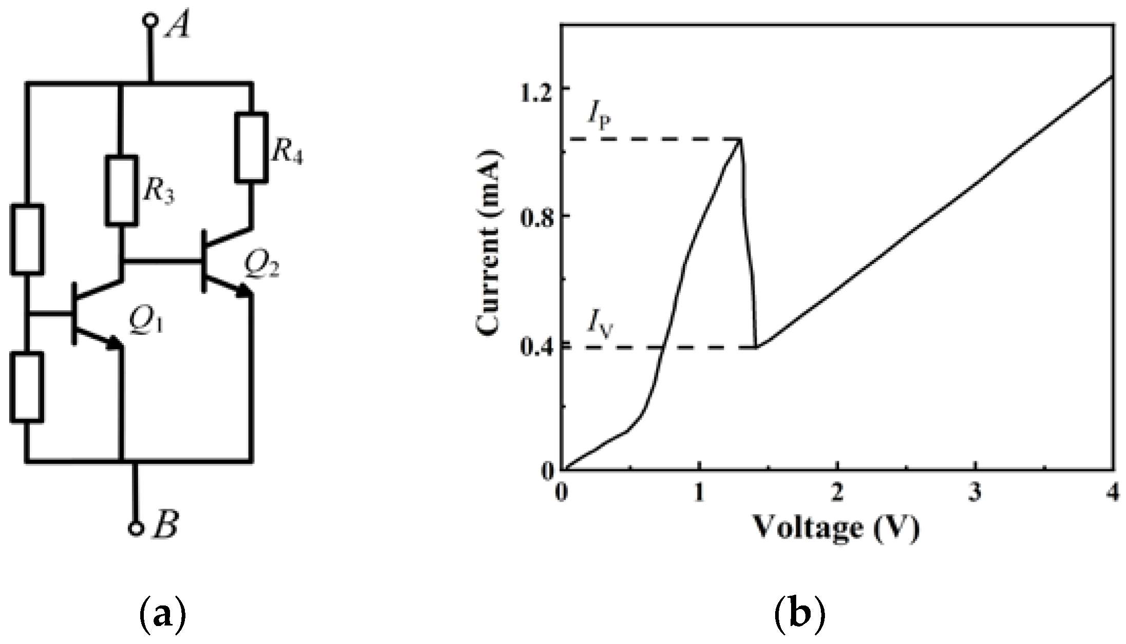
Kwang-Jow Gan proposed an R-HBT-NDR unit [28,29,30] with negative resistance characteristics, as shown in Figure 1.
When a sinusoidal signal VAB is applied to the R-HBT-NDR unit, its i-v characteristic curve has a certain hysteresis, as shown in Figure 2 [31].
With the increase in VAB, transistor Q2 turns on first, and then transistor Q1; the current flowing through the R-HBT-NDR unit increases. When VAB continues to increase, Q1 reaches the saturated state, which triggers Q2 to turn off. The current flowing through the R-HBT-NDR unit then decreases considerably from IP to IV, where negative resistance appears. With the further increase of VAB, Q2 remains off, while Q1 enters into the deep saturation state, and the current flowing through the R-HBT-NDR unit increases slowly with the change of the input signal VAB.
When VAB starts to decrease, Q1 enters the cut-off state; Q2 turns on, and then the current flowing through the R-HBT-NDR unit will increase. As the input signal continues to decrease, Q2 turns off to end.
Therefore, the movement path of the operation points differs with the increase and decrease of VAB, resulting in a hysteresis loop.
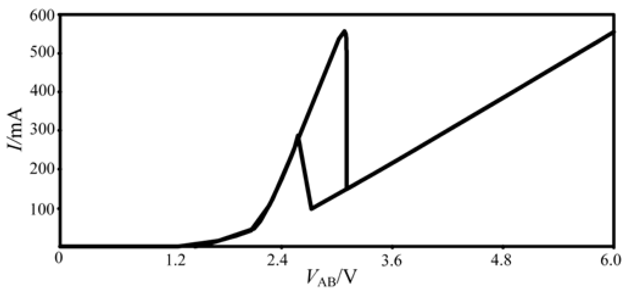
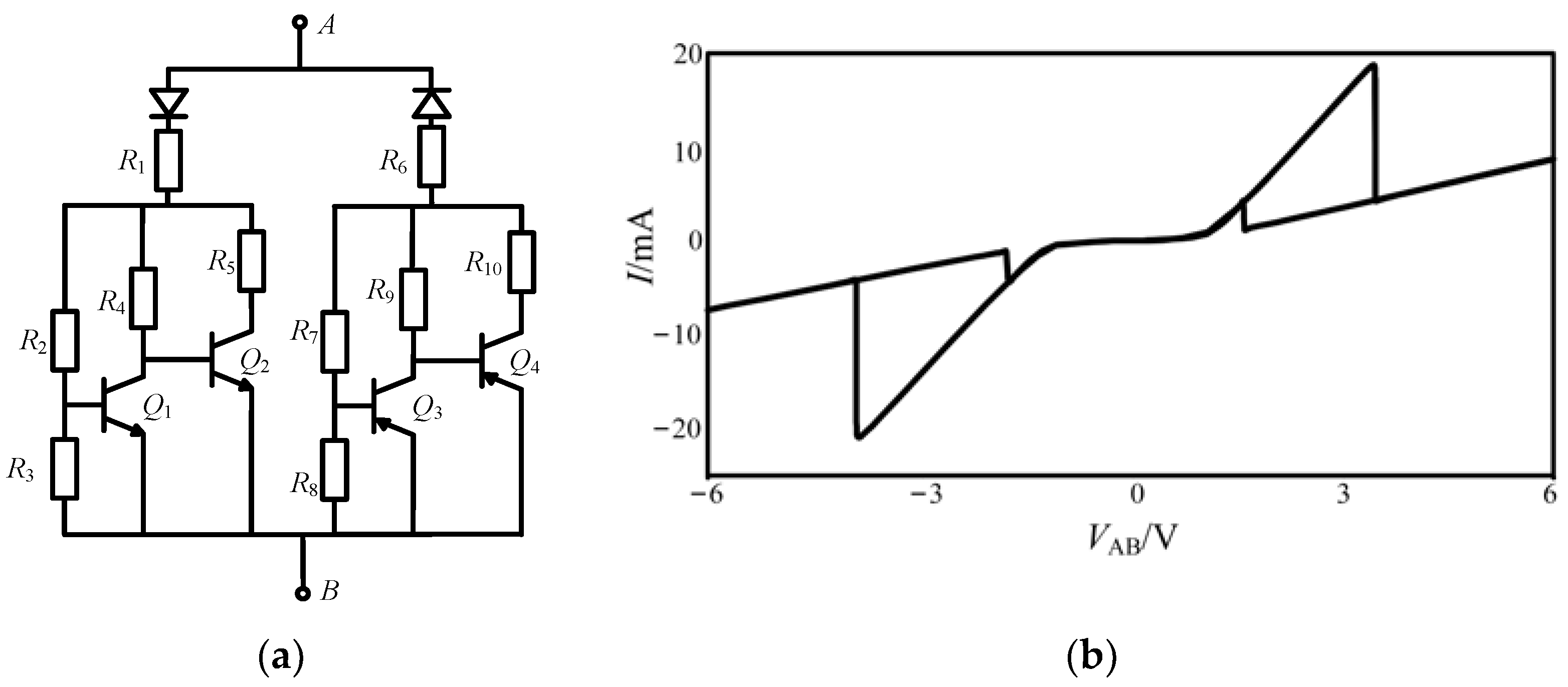
Figure 2 only presents the forward part of the curve because of the feature of the NPN transistor. If an extra R-HBT-NDR unit is implemented in the circuit, which consists of PNP bipolar transistors, shown as Figure 3a, under the excitation of the sinusoidal signal, the bidirectional hysteresis curve can be obtained, as shown in Figure 3b.
It can be seen from Figure 3b that the characteristic curve of the bidirectional NDR hysteresis unit shows two hysteresis loops. Meanwhile, the curve has a slope of 0 near the origin, indicating that the change of VAB will not affect the resistance, which can be attributed to the influence of the transistor turn-on voltage. Therefore, an improved NDR hysteresis unit is realized, as shown in Figure 4a, and its simplified symbol can be expressed as Figure 4b.
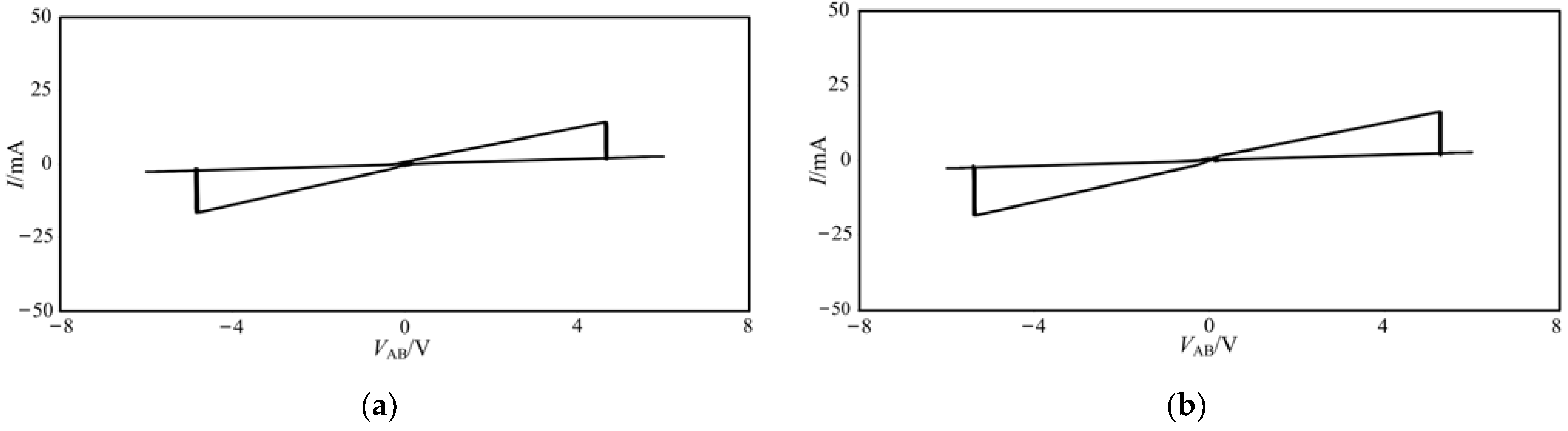
The improved NDR hysteresis unit differentiates its structure from Figure 3a in its two terminals of V+ and V−, which have the same voltage magnitude and opposite signs. With the change of V+ and V−, the bias voltage of each device in the NDR hysteresis unit will change accordingly, resulting in the different shape of the output curve, as shown in Figure 5.
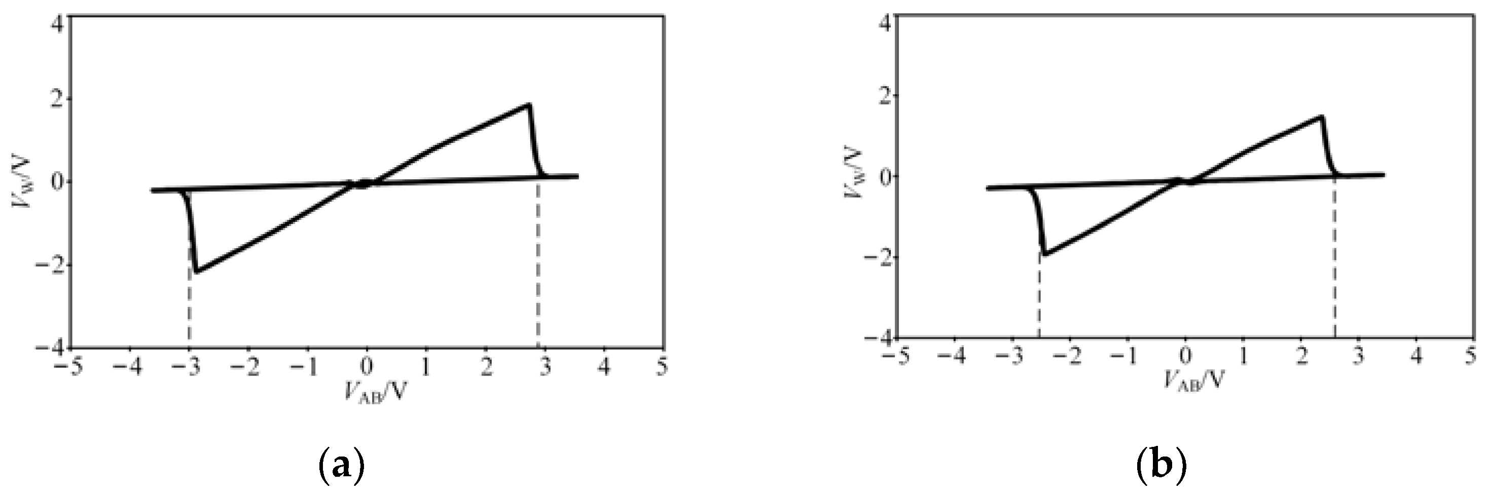
In Figure 5a, V+ = − V− = 2 V, it can be seen that when VAB = −4.8 V or 4.6 V, the state of the hysteresis curve is changed. In Figure 5b, V+ = − V− = 6 V, when VAB = −5.4 V or 5.3 V, the state of the hysteresis curve is changed.
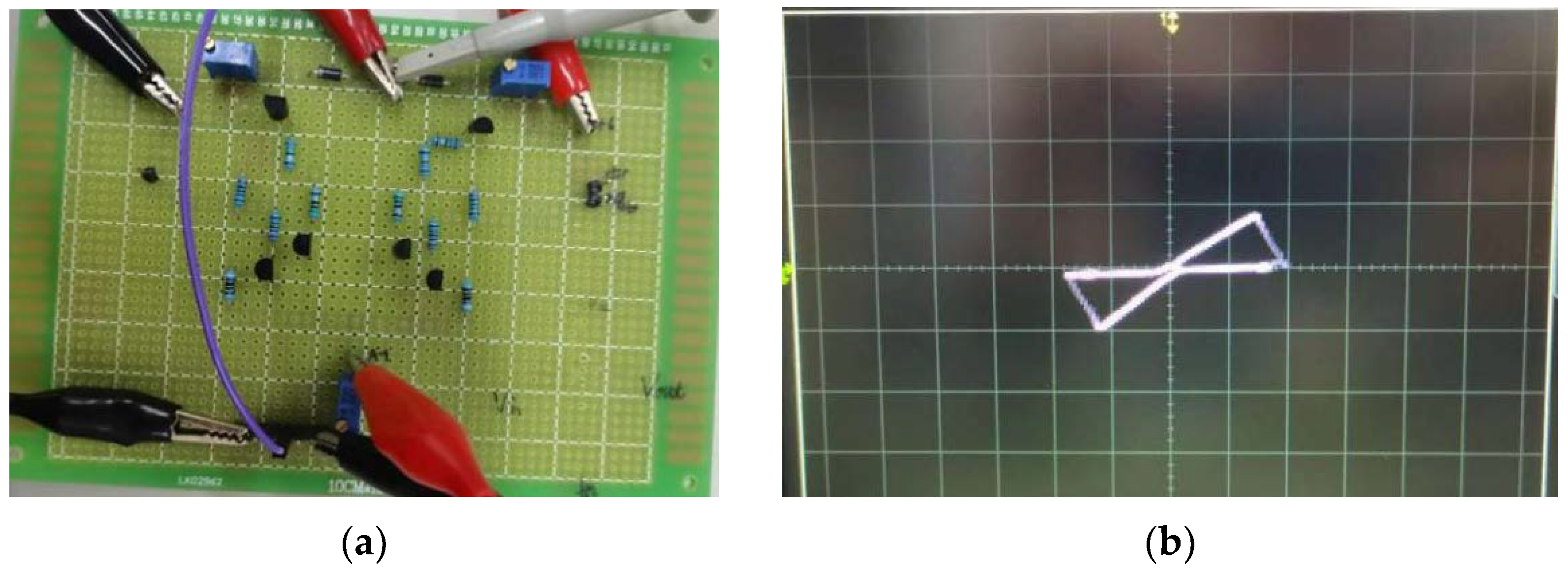
A hardware circuit of the improved NDR hysteresis unit is completed, as shown in Figure 6a. A resistor is connected in series as a load, and the current can be observed by measuring the voltage on the load resistor. Under the excitation of a sinusoidal signal with an amplitude of 6 V and a frequency of 5 kHz, V+ = V1 = 6 V, V− = V2 = −6 V, R1 = R7 = 10 Ω, R2 = 240 Ω, R3 = R5 = R9 = R11 = 2 kΩ, R4 = R10 = 8.8 kΩ, R6 = R12 = 50 Ω, R8 = 280 Ω. The experimental results are coincident with the simulation results.
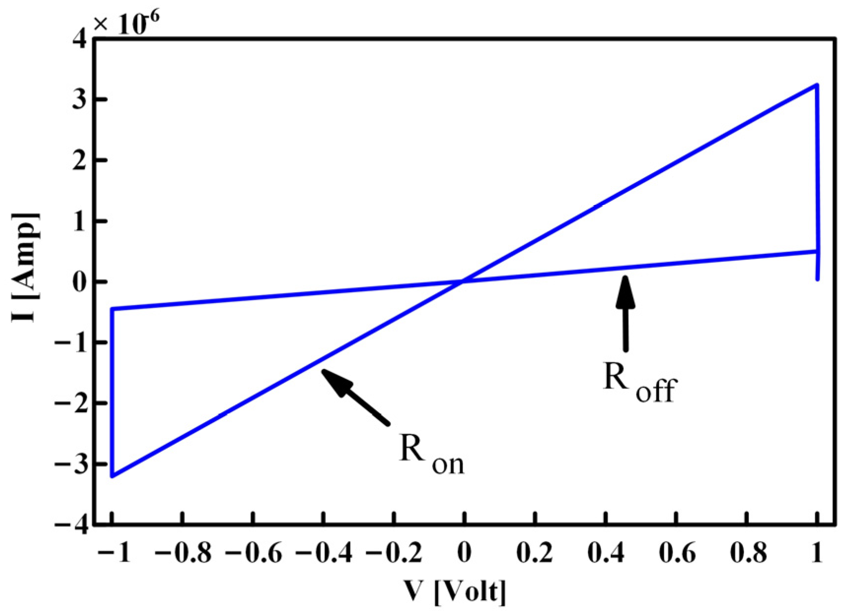
By analyzing the curve in Figure 6, it can be found that it is very similar to the i-v curve of the TEAM threshold memristor proposed in 2013 [32], shown in Figure 7.
The definition of the threshold type memristor can be expressed as follows [25]:
G is the memductance of the threshold memristor, with GH and GL corresponding to the two resistance states of the memristor: low resistance (LRS) and high resistance (HRS), respectively. Vth1 and Vth2 represent the threshold voltages of the memristor. When the voltage VX applied to the memristor is greater than Vth1, the memristor switches to GH; when the voltage VX is less than Vth2, the memristor is switched to GL; if the voltage applied to the memristor is between Vth1 and Vth2, the state of the memristor remains unchanged.
The hysteresis characteristic curve of the improved NDR hysteresis unit is so similar to the threshold-type memristor that we can utilize this unit to design a novel NDR memristor emulator. This is where the inspiration of this paper originates.
3. Circuit Structure Analysis of Threshold-Controllable Memristor Based on NDR Unit
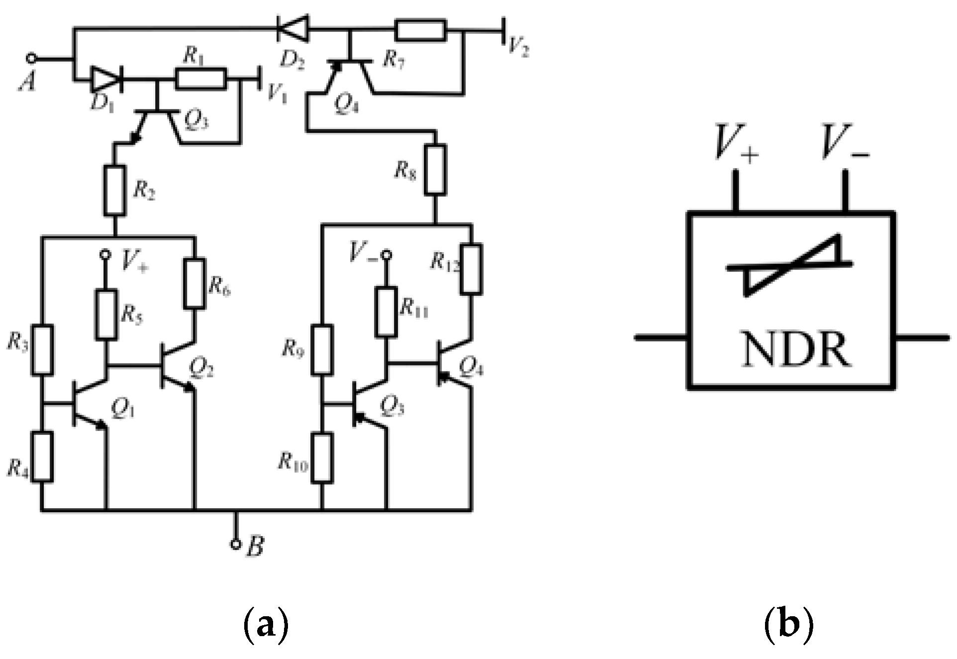
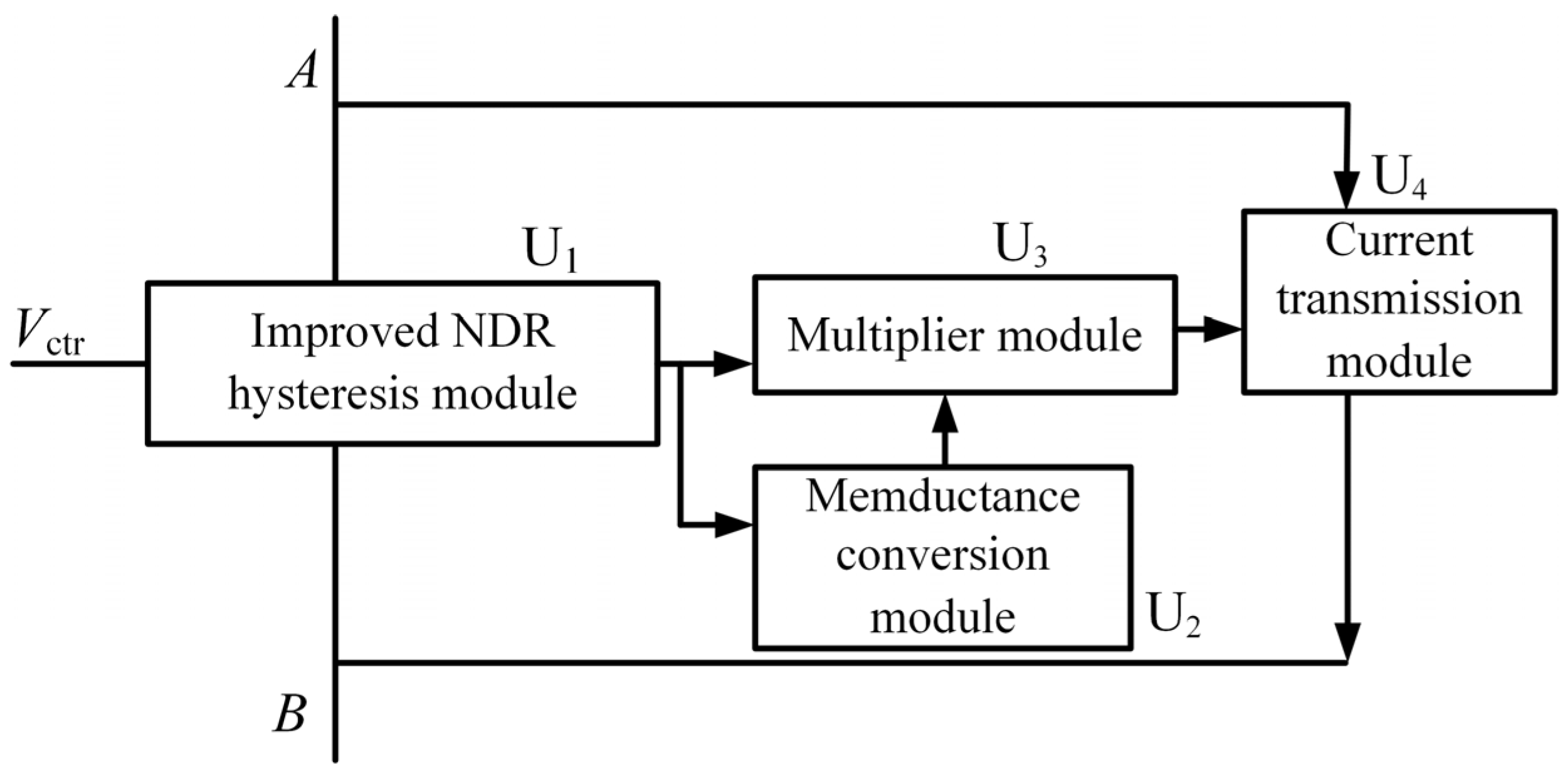
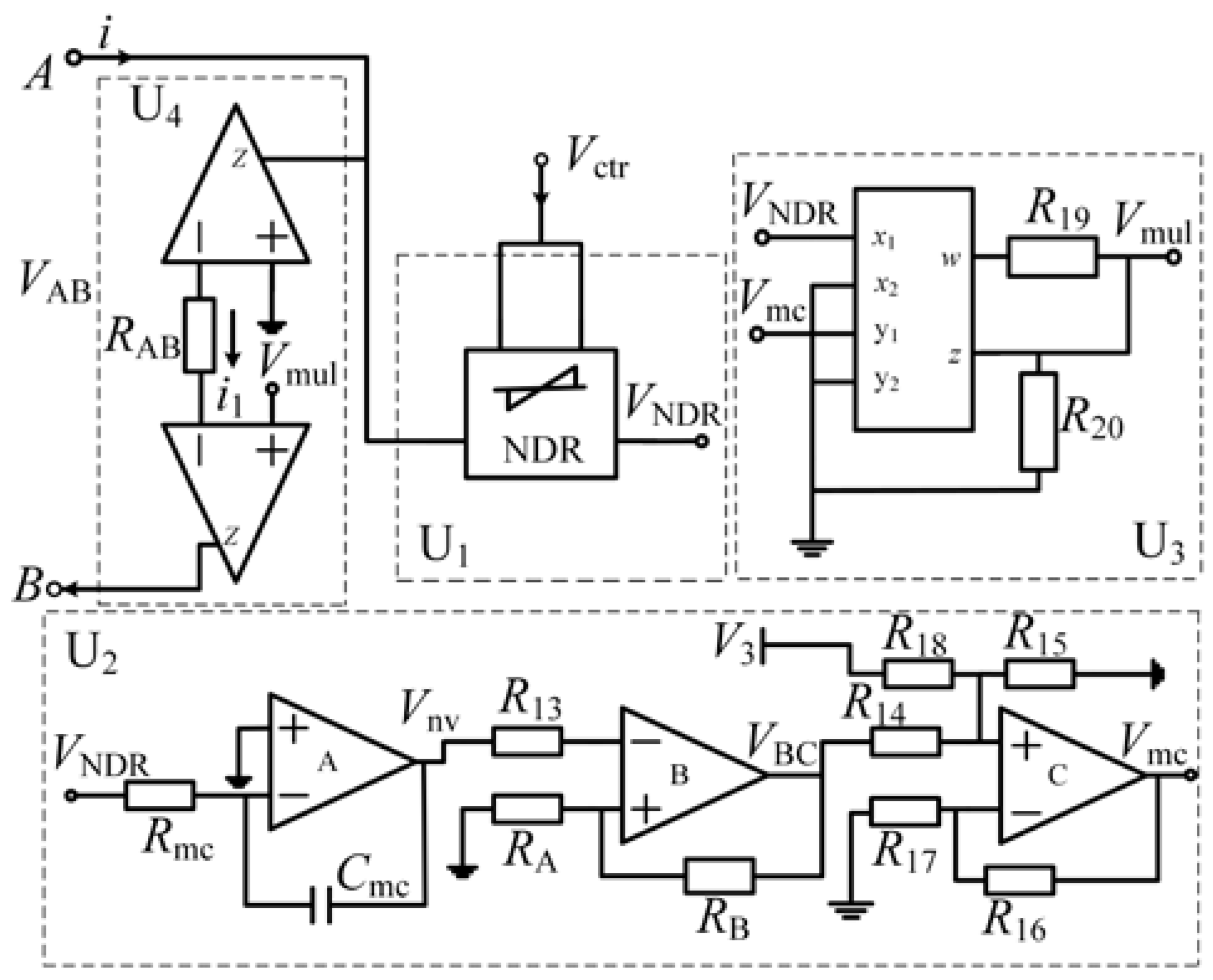
A diagram of the threshold-controllable memristor based on the NDR unit is shown in Figure 8, with an improved bidirectional NDR hysteresis module as the core. It also includes the memductance conversion module, multiplier module, and current transmission module.
The improved NDR hysteresis module U1 realizes the hysteresis characteristics; the memductance conversion module U2 realizes the non-volatile and high and low resistance conversion characteristics of the memristor; the multiplier module U3 converts the current of the memristor into a proportional voltage; the current transmission module U4 ensures the equal flow of the current at either end of the memristor.
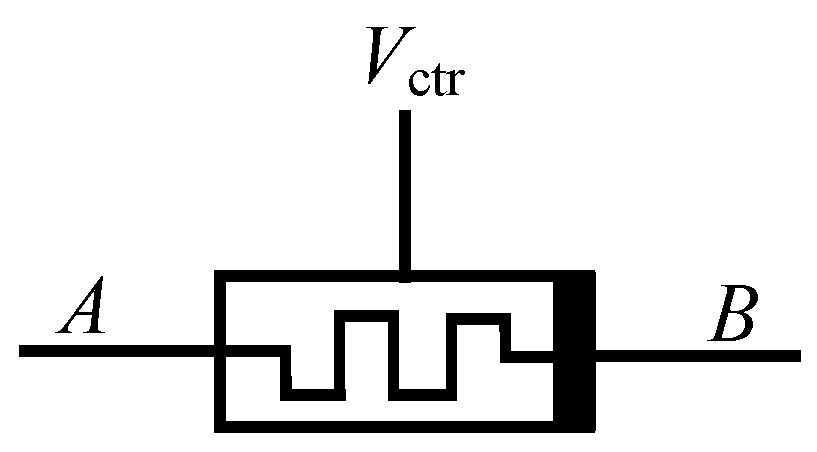
Vctr, represented by V+ and V− in Figure 4, is the control voltage. According to the above analysis, by changing the voltage of Vctr, the threshold of the memristor will also be changed to realize the change of the memristor resistance state. The symbol of the threshold-controllable memristor emulator can be expressed in a simplified form, as shown in Figure 9.
4. Circuit Design of Threshold-Controllable Memristor
The threshold-controllable memristor emulator circuit based on the improved NDR hysteresis unit is shown in Figure 10. The specific analysis of each module is as follows.
4.1. Improved NDR Hysteresis Module U1
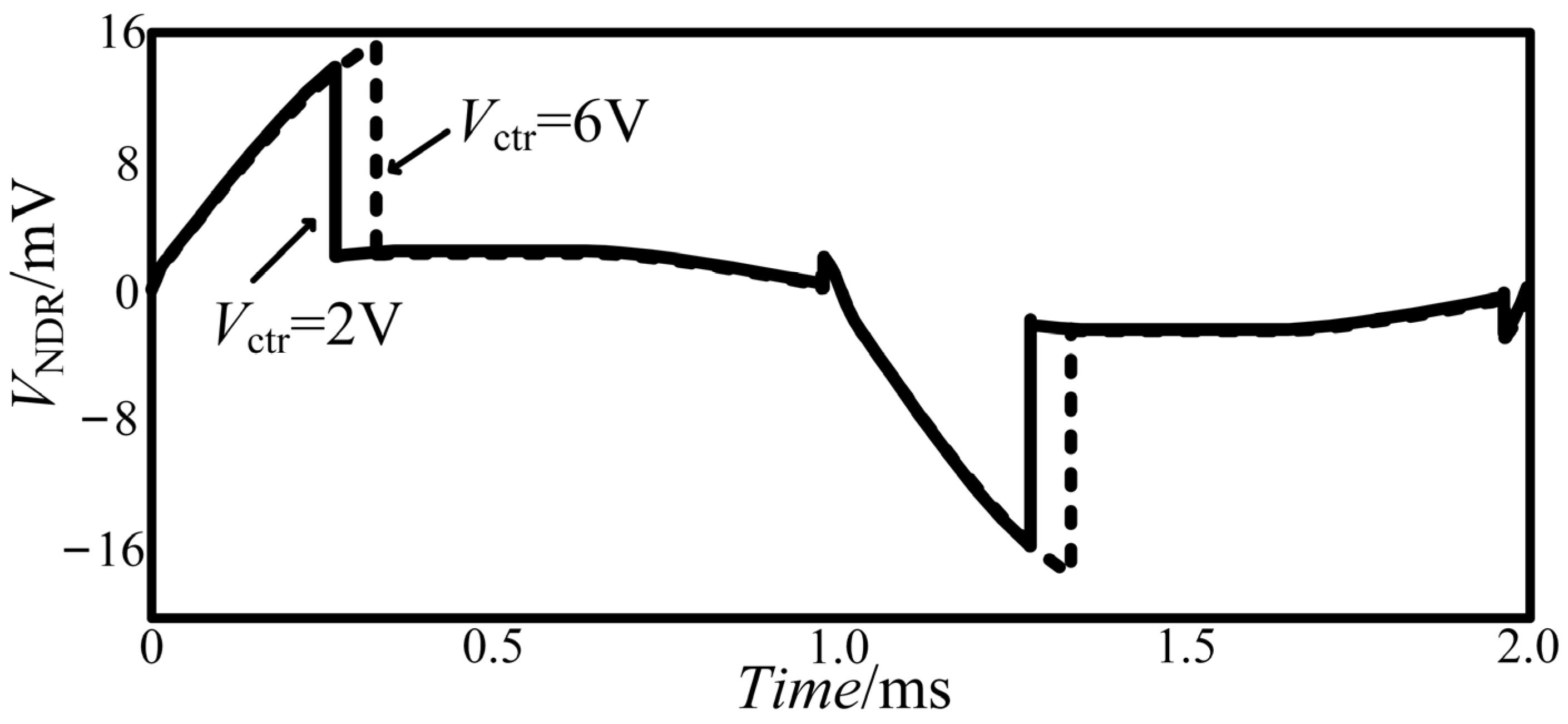
U1 is the improved NDR hysteresis module. Vctr is a threshold control terminal. When Vctr changes, the change trajectories of output VNDR are shown in Figure 11. The input voltage is a sinusoidal signal with an amplitude of 6 V and a frequency of 5 kHz.
A relationship is found between Vctr and VNDR: when Vctr increases, VNDR will increase accordingly, which can be expressed as:
4.2. Memductance Conversion Module U2
U2 is the memductance conversion module, composed of a four-channel operational amplifier TL084, a capacitor, and several resistors, which is used to achieve the non-volatile and high/low resistance characteristics of memristors. The output VNDR of U1 is the input signal of U2.
Since the memristor has the non-volatile characteristic, its resistance must be related to the previous state. Rmc and Cmc form the integrator with the output Vnv of:
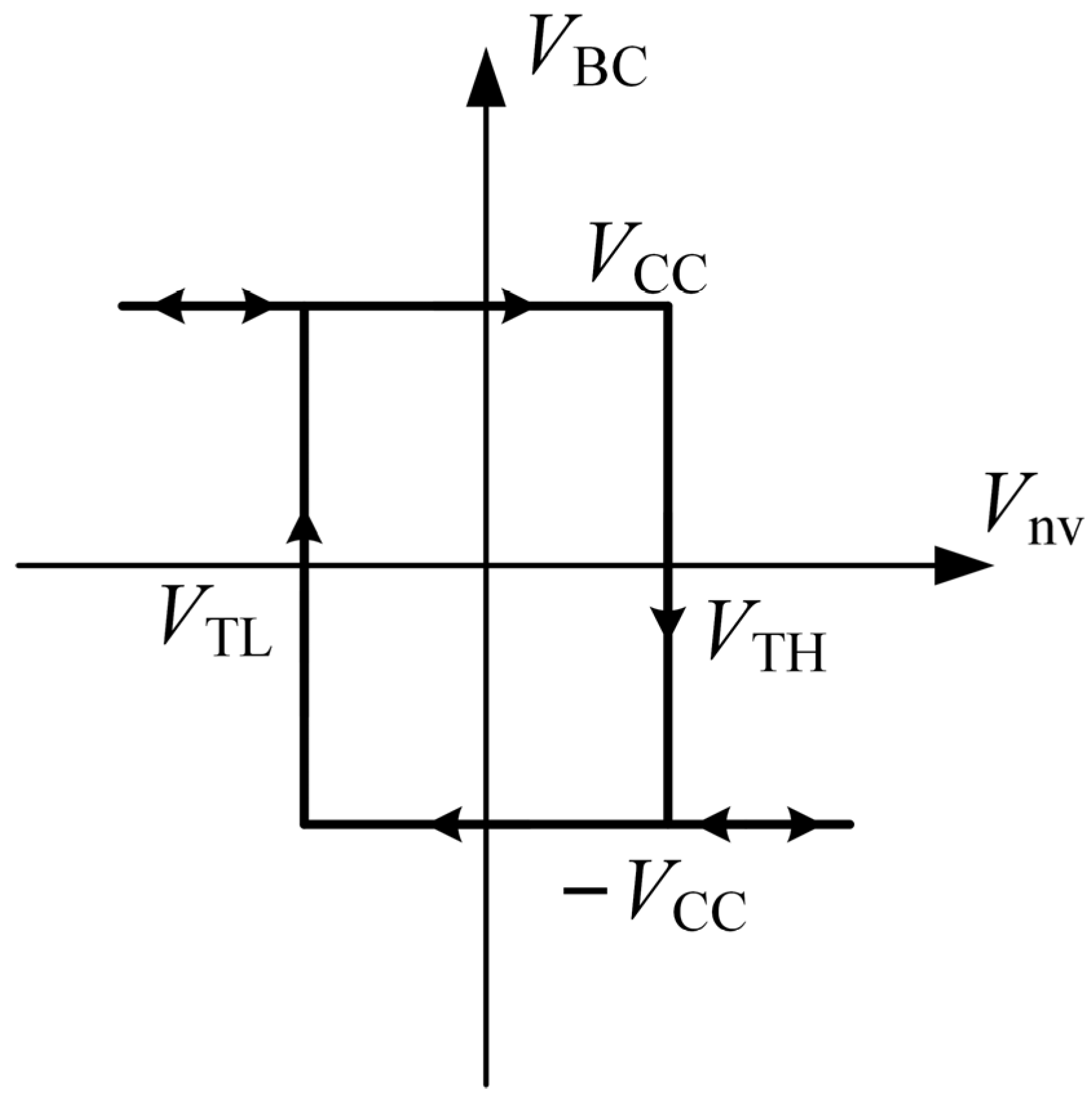
Figure 12 presents the characteristics of the bistable circuit that is composed of part B of TL084.
In Figure 12, when Vnv is greater than VTH, the output is −VCC; when Vnv is less than VTL, the output is VCC; when Vnv is between VTL and VTH, the state will not change. −VCC and VCC represent the power supply voltages of TL084. Therefore, the output voltage VBC of the bistable circuit is expressed as follows:
and the threshold voltages of VTH and VTL are expressed as follows:
In addition, in order to achieve the single polarity for the output voltage of Vmc, a summing circuit is constructed, which consists of part C of TL084, V3, R14, R15, R16, R17, and R18. The corresponding output Vmc is expressed as follows:
where a = R16/R14, b = R16/R15; compared to the definition of the threshold-type memristor in (1), (aVCC + bV3) can be seen as a voltage representation of the high-memductance state of memristor; (bV3 − aVCC) can be seen as a voltage representation of the low-memductance state of the memristor.
4.3. Multiplier Module U3
U3 is the multiplier module and it is composed of a multiplier AD633, which converts the current of the memristor into a proportional voltage. The output of U3 can be expressed as follows:
where VNDR is the output of U1 and Vmc is the output of U2. R19 and R20 adjust the multiplication coefficient.
4.4. Current Transmission Module U4
U4 is the current transmission module and composed of two AD844 operational amplifiers. This module converts the voltage Vmul into the corresponding current and ensures equal currents flowing through A and B terminals. The current through the memristor is expressed as follows:
and the current flowing through RAB is i1 = VAB/RAB; therefore, the memductance G can be represented by the voltage Vmc, as follows:
Assuming kG = (R19 + R20)/(10R19i1) = (R19 + R20)/(10R19i1), G can also be expressed as:
Therefore, the mathematical emulator of the memristor emulator circuit can be expressed as follows:
Compared with Equation (1), G in Equation (11) satisfies the definition of threshold memristors. In addition, when the value of Vctr changes, G changes, with the threshold-controllable function thereby being achieved.
5. Verification of Threshold-Controllable Memristor
5.1. Simulation Results
The simulation results of the threshold-controllable memristor are shown in Figure 13: R1 = R7 = 19 Ω, R2 = 7.5 Ω, R3 = R5 = R9 = R11 = 2 kΩ, R4 = R10 = 8 kΩ, R6 = R12 = 51 Ω, R8 = 29 Ω, R13 = 1 Ω, R14 = 9.1 kΩ, R15 = 1 kΩ, R16 = 10 kΩ, R17 = R18 = 1 kΩ, R19 = 10 kΩ, R20 = 5.6 kΩ, Rmc = 10 kΩ, Cmc = 1 nF, RA = 0.5 kΩ, RB = 2.5 kΩ, RAB = 100 kΩ. The excitation signal is a sinusoidal signal with a 5 V amplitude 30 kHz frequency.
When Vctr = 6 V, the threshold voltage of the memristor is about ±2.9 V; when Vctr = 2 V, the threshold voltage is −2.6 V and 2.7 V. Therefore, when Vctr changes, the memristor threshold voltage changes accordingly. This feature can be applied to digital logic circuits design where the state of the memristor can switch to high or low in order for varied logic states by only changing Vctr, and different functions will be achieved without modifying the circuit structure and input signals.
5.2. Experimental Results
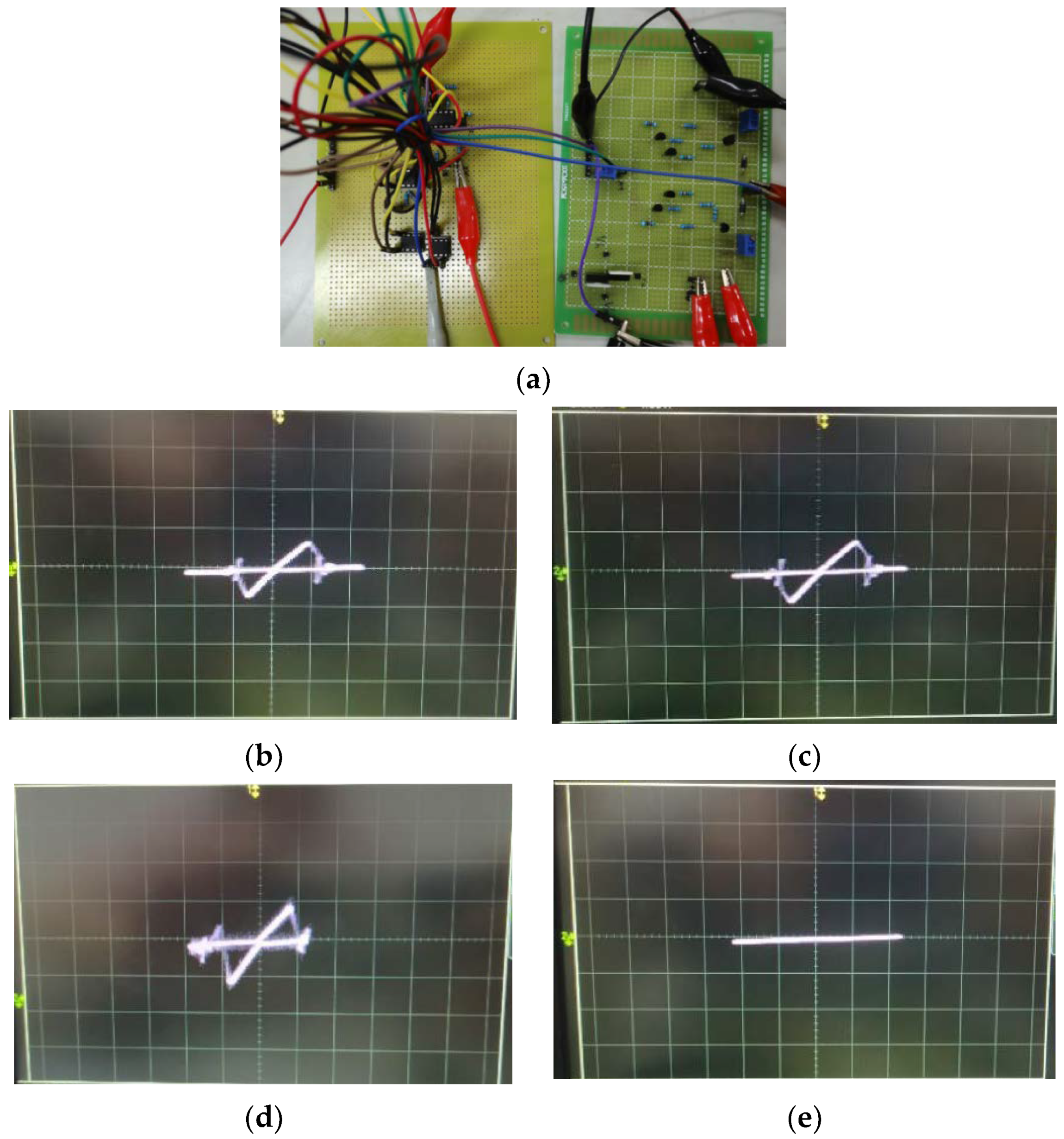
The hardware circuit of the threshold-controllable memristor emulator based on NDR characteristics and its experimental results is shown in Figure 14.
Under the excitation of a sinusoidal signal with an amplitude of 6 V and a frequency of 72 kHz, when Vctr = 2 V, its threshold voltages are −2 V and 2.1 V, as shown in Figure 14b. When Vctr = 6 V, its threshold is about −2.2 V and 2.8 V, as in Figure 14c. If the frequency keeps increasing until 345 kHz, the hysteresis loop will be missing and the non-volatile characteristic disappears, as in Figure 14e.
6. Conclusions
A threshold-controllable memristor emulator based on NDR characteristics is proposed, which is composed of an improved NDR hysteresis unit, multipliers, and operational amplifiers. In addition to the basic characteristics of memristors such as being non-volatile and non-linear, this emulator circuit also has the advantage of threshold controllability and high operating frequency. Compared to the two-terminal structure of the traditional memristor, the threshold-controllable memristor emulator is more suitable for digital circuit design thanks to its additional control terminal structure, where the memristor threshold switches under different control voltages, indicating more flexible and convenient memristor-based circuit designs. Our follow-up effort will be committed to continuously optimizing the performance of the emulator, and the attempt to apply it to the design of memristive digital logic circuits.
Author Contributions
Conceptualization, writing, review, visualization: M.L.; simulation, experiment: W.L. (Wenyao Luo); methodology, data curation: L.L.; formal analysis: Q.H.; investigation, supervision: W.L. (Weifeng Lyu). All authors have read and agreed to the published version of the manuscript.
Funding
This research was funded by the National Natural Science Foundation of China (62071160).
Conflicts of Interest
The authors declare no conflict interest.
References
- Chua, L.O. Memristor-the missing circuit element. IEEE Trans. Circuit Theory 1971, 5, 507–519. [Google Scholar] [CrossRef]
- Strukov, D.; Snider, G.; Stewart, D.; Williams, R. The missing memristor found. Nature 2008, 453, 80–83. [Google Scholar] [CrossRef] [PubMed]
- Mohanty, N.; Dey, R.; Roy, B. A new 3-D memristive time-delay chaotic system with multi-scroll and hidden attractors. IFAC 2018, 51, 580–585. [Google Scholar] [CrossRef]
- Xiaoyuan, W.; Meng, G.; Herbert, H.L.; Chunhua, W. Tri-valued Memristor-based Hyper-chaotic System with Hidden and Coexistent Attractors. Chaos Solitons Fractals 2022, 159, 112177. [Google Scholar] [CrossRef]
- Zhuosheng, L.; Guangyi, W.; Xiaoyuan, W.; Simin, Y.; Jinhu, L. Security performance analysis of a chaotic stream cipher. Nonlinear Dyn. 2018, 94, 1003–1017. [Google Scholar]
- John, R.A.; Demirağ, Y.; Shynkarenko, Y. Reconfigurable halide perovskite nanocrystal memristors for neuromorphic computing. Nat. Commun. 2022, 13, 2074. [Google Scholar] [CrossRef]
- Sun, J.; Kang, K.; Sun, Y. A multi-value 3D crossbar array nonvolatile memory based on pure memristors. Eur. Phys. J. Spec. Top. 2022, 1–12. [Google Scholar] [CrossRef]
- Wang, X.-Y.; Zhou, P.-F.; Eshraghian, J.K.; Lin, C.-Y.; Iu, H.H.-C.; Chang, T.-C.; Kang, S.-M. High-Density Memristor-CMOS Ternary Logic Family. IEEE Trans. Circuits Syst. I Regul. Pap. 2021, 68, 264–274. [Google Scholar] [CrossRef]
- Xiaoyuan, W.; Zhiru, W.; Pengfei, Z.; Herbert, H.L.; Sung, M.K.; Jason, K.E. FPGA Synthesis of Ternary Memristor-CMOS Decoders for Active Matrix Microdisplays. IEEE Trans. Circuits Syst. I Regul. Pap. 2022, 1–11. [Google Scholar] [CrossRef]
- Eshraghian, J.K.; Lin, Q.; Wang, X.; Iu, H.H.C.; Hu, Q.; Tong, H. A Behavioral Model of Digital Resistive Switching for Systems Level DNN Acceleration. IEEE Trans. Circuits Syst. II Express Briefs 2020, 67, 956–960. [Google Scholar] [CrossRef]
- Hairong, L.; Chunhua, W.; Chengjie, C.; Yichuang, S.; Chao, Z.; Cong, X.; Qinghui, H. Neural bursting and synchronization emulated by neural networks and circuits. IEEE Trans. Circuits Syst. I Regul. Pap. 2021, 68, 3397–3410. [Google Scholar]
- Mei, G.; Yongliang, Z.; Renyuan, L.; Kaixuan, Z.; Gang, D. An associative memory circuit based on physical memristors. Neurocomputing 2022, 472, 12–23. [Google Scholar] [CrossRef]
- Prezioso, M.; Merrikh-Bayat, F.; Hoskins, B.D.; Adam, G.C.; Likharev, K.K.; Strukov, D.B. Training and operation of an integrated neuromorphic network based on metaloxide memristors. Nature 2015, 521, 61–64. [Google Scholar] [CrossRef] [PubMed]
- Babacan, Y.; Yesil, A.; Gul, F. The Fabrication and MOSFET-Only Circuit Implementation of Semiconductor Memristor. IEEE Trans. Electron Devices 2018, 65, 1–8. [Google Scholar] [CrossRef]
- Li, P.; Wang, X.; Zhang, X. Spice modelling of a tri-state memristor and analysis of its series and parallel characteristics. IET Circuits Devices Syst. 2022, 16, 81–91. [Google Scholar] [CrossRef]
- Huang, L.X.; Yu, H.Q.; Chen, C.L.; Peng, J.; Diao, J.T.; Nie, H.S.; Li, Z.W.; Liu, H.J. A training strategy for improving the robustness of memristor-based binarized convolutional neural networks. Semicond. Sci. Technol. 2022, 37, 015013. [Google Scholar] [CrossRef]
- Fitch, A.L.; Iu, H.C.; Wang, X.Y. Realization of an analog model of memristor based on light dependent resistor. In Proceedings of the IEEE Symposium on Circuits and Systems (ISCAS), Seoul, Korea, 20–23 May 2012; pp. 1139–1142. [Google Scholar] [CrossRef]
- Petrović, P.B. Charge-controlled grounded memristor emulator circuits based on Arbel-Goldminz cell with variable switching behaviour. Analog. Integr. Circuits Signal Process. 2022, 1–9. [Google Scholar] [CrossRef]
- Raj, A.; Singh, S.; Kumar, P. Dual mode, high frequency and power efficient grounded memristor based on OTA and DVCC. Analog. Integr. Circuits Signal Process. 2022, 110, 81–89. [Google Scholar] [CrossRef]
- Abuelma’atti, M.T.; Khalifa, Z.J. A new memristor emulator and its application in digital modulation. Analog. Integr. Circuits Signal Process. 2014, 80, 577–584. [Google Scholar] [CrossRef]
- Ahmer, M.; Kidwai, N.R.; Yasin, M.Y. Memristor emulation and analog application using differential difference current conveyor of CC-II in CMOS technology. Mater. Today Proc. 2022, 51, 234–239. [Google Scholar] [CrossRef]
- Gozukucuk, M.M.; Menekay, S.; Ozenli, D. A Novel Fully Floating Memristor Emulator Using OTA and Passive Elements. In Proceedings of the 2021 13th International Conference on Electrical and Electronics Engineering (ELECO), Bursa, Turkey, 25–27 November 2021; pp. 29–33. [Google Scholar] [CrossRef]
- Yunus, B.; Abdullah, Y.; Firat, K. Memristor emulator with tunable characteristic and its experimental results. AEU Int. J. Electron. Commun. 2017, 81, 99–104. [Google Scholar] [CrossRef]
- Petrović, P.B. Floating incremental/decremental flux-controlled memristor emulator circuit based on single VDTA. Analog. Integr. Circuits Signal Process. 2018, 96, 417–433. [Google Scholar] [CrossRef]
- Yesil, A.; Babacan, Y.; Kacar, F. Electronically tunable memristor based on VDCC. AEU-Int. J. Electron. Commun. 2019, 107, 282–290. [Google Scholar] [CrossRef]
- Liang, Y.; Lu, Z.; Wang, G.; Yu, D.; Lu, H.H. Threshold-type binary memristor emulator Circuit. IEEE Access 2019, 7, 180181–180193. [Google Scholar] [CrossRef]
- Knowm Inc. Available online: https://knowm.org (accessed on 9 May 2019).
- Gan, K.; Tsai, C.; Liang, D.; Tu, C.; Chen, Y. Multiple-input NOR logic design using negative differential resistance circuits implemented by standard SiGe process. Solid State Electron. 2008, 52, 175–178. [Google Scholar] [CrossRef]
- Gan, K.; Su, Y. Novel multipeak current-voltage characteristics of series-connected negative differential resistance devices. IEEE Electron Device Lett. 1998, 19, 109–111. [Google Scholar] [CrossRef]
- Gan, K. The low-high-low I-V characteristics of five to seven peaks based on four NDR devices. IEEE Trans. Electron Devices 2001, 48, 1683–1687. [Google Scholar] [CrossRef]
- Mi, L.; Qiao, W.; Weifeng, L. Design of multiple-valued logic unit by using R-HBT-NDR-based memristor. FSDM 2019, 945–950. [Google Scholar] [CrossRef]
- Kvatinsky, S.; Friedman, E.; Kolodny, A. TEAM: Threshold adaptive memristor model. IEEE Trans. Circuits Syst. I Regul. Pap. 2013, 60, 211–221. [Google Scholar] [CrossRef]
Figure 1.
R-HBT-NDR unit and its i-v characteristic curve: (a) R-HBT-NDR unit, (b) the i-v characteristic curve of R-HBT-NDR unit.
Figure 1.
R-HBT-NDR unit and its i-v characteristic curve: (a) R-HBT-NDR unit, (b) the i-v characteristic curve of R-HBT-NDR unit.

Figure 2.
Hysteresis characteristic of the R-HBT-NDR unit.

Figure 3.
Bidirectional NDR hysteresis unit and its i-v characteristic curve: (a) bidirectional NDR hysteresis unit, (b) the i-v characteristic curve of bidirectional NDR hysteresis unit.
Figure 3.
Bidirectional NDR hysteresis unit and its i-v characteristic curve: (a) bidirectional NDR hysteresis unit, (b) the i-v characteristic curve of bidirectional NDR hysteresis unit.

Figure 4.
Improved NDR hysteresis circuit and its simplified symbol: (a) improved NDR hysteresis circuit, (b) the simplified symbol of improved NDR hysteresis circuit.
Figure 4.
Improved NDR hysteresis circuit and its simplified symbol: (a) improved NDR hysteresis circuit, (b) the simplified symbol of improved NDR hysteresis circuit.

Figure 5.
The i-v characteristic curve of the improved hysteresis circuit: (a) when V+ = − V− = 2 V, (b) when V+ = − V− = 6 V.
Figure 5.
The i-v characteristic curve of the improved hysteresis circuit: (a) when V+ = − V− = 2 V, (b) when V+ = − V− = 6 V.

Figure 6.
Improved NDR hysteresis unit hardware circuit and its experimental result: (a) improved NDR hysteresis unit hardware circuit, (b) experimental result.
Figure 6.
Improved NDR hysteresis unit hardware circuit and its experimental result: (a) improved NDR hysteresis unit hardware circuit, (b) experimental result.

Figure 7.
The i-v characteristic curve of the TEAM threshold type memristor.

Figure 8.
Diagram of threshold-controllable memristor emulator based on NDR units.

Figure 9.
Simplified symbol of threshold-controllable memristor.

Figure 10.
Threshold-controllable memristor emulator circuit based on the improved NDR hysteresis unit.
Figure 10.
Threshold-controllable memristor emulator circuit based on the improved NDR hysteresis unit.

Figure 11.
Output curves of VNDR.

Figure 12.
Characteristics of the bistable circuit composed of part B of TL084.

Figure 13.
Simulation curves: (a) Vctr = 6 V, (b) Vctr = 2 V.

Figure 14.
Hardware circuit and experimental results: (a) the circuit of the threshold-controllable memristor emulator, (b) Vctr = 2 V, f = 72 kHz, (c) Vctr = 6 V, f = 72 kHz, (d) Vctr = 6 V, f = 250 kHz, (e) Vctr = 6 V, f = 345 kHz.
Figure 14.
Hardware circuit and experimental results: (a) the circuit of the threshold-controllable memristor emulator, (b) Vctr = 2 V, f = 72 kHz, (c) Vctr = 6 V, f = 72 kHz, (d) Vctr = 6 V, f = 250 kHz, (e) Vctr = 6 V, f = 345 kHz.

Publisher’s Note: MDPI stays neutral with regard to jurisdictional claims in published maps and institutional affiliations. |
© 2022 by the authors. Licensee MDPI, Basel, Switzerland. This article is an open access article distributed under the terms and conditions of the Creative Commons Attribution (CC BY) license (https://creativecommons.org/licenses/by/4.0/).
Share and Cite
MDPI and ACS Style
Lin, M.; Luo, W.; Li, L.; Han, Q.; Lyu, W. Design of the Threshold-Controllable Memristor Emulator Based on NDR Characteristics. Micromachines 2022, 13, 829. https://0-doi-org.brum.beds.ac.uk/10.3390/mi13060829
AMA Style
Lin M, Luo W, Li L, Han Q, Lyu W. Design of the Threshold-Controllable Memristor Emulator Based on NDR Characteristics. Micromachines. 2022; 13(6):829. https://0-doi-org.brum.beds.ac.uk/10.3390/mi13060829
Chicago/Turabian StyleLin, Mi, Wenyao Luo, Luping Li, Qi Han, and Weifeng Lyu. 2022. "Design of the Threshold-Controllable Memristor Emulator Based on NDR Characteristics" Micromachines 13, no. 6: 829. https://0-doi-org.brum.beds.ac.uk/10.3390/mi13060829
Note that from the first issue of 2016, this journal uses article numbers instead of page numbers. See further details here.