
Tuning Structural Properties of WO3 Thin Films for Photoelectrocatalytic Water Oxidation
by
 , and
, and
Amar Kamal Mohamedkhair
1,2, 
Qasem Ahmed Drmosh
2,
Mohammad Qamar
2,3,* and
Zain Hassan Yamani
1,2 1
Physics Department, King Fahd University of Petroleum and Minerals, Dhahran 31261, Saudi Arabia
2
Center of Research Excellence in Nanotechnology (CENT), King Fahd University of Petroleum and Minerals, Dhahran 31261, Saudi Arabia
3
K.A.CARE Energy Research & Innovation Center, King Fahd University of Petroleum and Minerals, Dhahran 31261, Saudi Arabia
*
Author to whom correspondence should be addressed.
Catalysts 2021, 11(3), 381; https://0-doi-org.brum.beds.ac.uk/10.3390/catal11030381
Submission received: 28 February 2021
/
Revised: 11 March 2021
/
Accepted: 14 March 2021
/
Published: 16 March 2021
(This article belongs to the Special Issue Photoelectrochemical and Photocatalytic Materials for Fuel Production)
Abstract
:The preparation of tungsten oxide (WO3) thin film by direct current (DC) reactive sputtering magnetron method and its photoelectrocatalytic properties for water oxidation reaction are investigated using ultraviolet-visible radiation. The structural, morphological, and compositional properties of WO3 are fine-tuned by controlling thin film deposition time, and post-annealing temperature and environment. The findings suggest that the band gap of WO3 can be controlled by adjusting the post-annealing temperature; the band gap decreased from 3.2 to 2.7 eV by increasing the annealing temperature from 100 to 600 °C. The theoretical calculations of the WO3 bandgap and the density of state are performed by density functional theory (DFT). Following the band gap modification, the photoelectrocatalytic activity increased and the maximum photocurrent (0.9 mA/cm2 at 0.6 VSCE) is recorded with WO3 film heated at 500 °C. The WO3 film heated under air exhibits much better performance in photoelectrochemical water oxidation process than that of annealed under inert atmosphere, due to its structural variation. The change in sputtering time leads to the formation of WO3 with varying film thickness, and the maximum photocurrent is observed when the film thickness is approximately 150 nm. The electrical conductivity and charge transfer resistance are measured and correlated to the properties and the performance of the WO3 photoelectrodes. In addition, the WO3 photoelectrode exhibits excellent photoelectrochemical stability.
1. Introduction
Hydrogen energy is considered as a potential solution for addressing the world’s energy needs. It represents a promising energy resource that can avert carbon dioxide emissions from fossil fuels [1,2,3]. The photoelectrocatalytic (PEC) technique is an auspicious method for the production of pure oxygen and hydrogen streams from water [4,5,6]. The PEC technique has gained attention mainly due to its advantages represented by positive environmental effect and low energy consumption [7,8,9]. Moreover, PEC uses suitable semiconductors with a bandgap equal to or lower than the solar absorbed photons to harvest solar energy [10,11,12,13,14].
Nowadays, many investigations are dedicated to application of metal oxide semiconductors, such as TiO2, ZnO, CuO, BiVO4, Fe2O4 etc., as photoanodes for photoelectro-chemical water oxidation [15,16,17,18,19]. Among these metal oxide semiconductors, tungsten oxide (WO3) has received much attention due to the wide range of its bandgap (~2.6 to ~2.8 eV for bulk material [20] and up to 3.2 eV for nanostructure forms [21]) that can absorb up to 480 nm, and hence being active in the visible light region.
The WO3 photoanode films can be deposited using various methods, such as hydrothermal, electrodeposition, spray pyrolysis, dip coating, and sputtering [22,23,24,25,26,27]. Among these deposition methods, the sputtering system is an effective deposition technique that can enable the tuning of thin film parameters by controlling the deposition power, gas atmosphere, working pressure, deposition angle, substrate temperature, and deposition time [28,29,30].
The deposition conditions during sputtering have a significant impact on the photoelectrocatalytic activity of WO3 films. For instance, Fendrich et al. [31] deposited WO3 films followed by post annealing at different temperatures. They found that the annealing temperature can affect the crystallinity, morphology, light absorption, and photocatalytic activity of the fabricated films. A similar evolution in morphological and structural properties of the WO3 nano-porous films, prepared by potentiostatic anodization, as a function of post-annealing temperature is reported by Mohamed et al. [32]. Specifically, the film’s crystallinity was improved at elevated annealing temperatures (300 °C and above). In addition, the optical properties, and the photocurrent density of the prepared films were dependent on the annealing temperature. Another crucial factor is the film thickness, which can be controlled by adjusting the deposition time. For example, Han et al. [33] found that the photocurrent density increased significantly by increasing the thickness of WO3 film, which was deposited by pulsed laser deposition (PLD). Similarly, Fang et al. [34] showed that an optimal thickness could give the highest photoelectrocatalytic activity. Exceeding that optimal thickness had negative impact on the PEC performance. Driven by these findings, attempted to perform a comprehensive study to investigate the influence of post-annealing temperature, annealing atmosphere, and deposition time on the photoelectrocatalytic activity of the WO3 sputtered thin films.
In this work, we fabricated WO3 thin films under different conditions using DC reactive sputtering system and studied their photoelectrocatalytic property by monitoring the water oxidation. The photoelectrocatalytic activity of these films was studied as a function of post-annealing temperature, annealing environment, and deposition time. Accordingly, the consequent changes in film’s characteristics, due to the change in fabrication condition, such as surface morphology, crystallinity, optical property, and resistivity, have been investigated and correlated with the PEC results. In addition, the theoretical bandgap of WO3 film was calculated using DFT calculation and then compared with the experimental value.
2. Results and Discussion
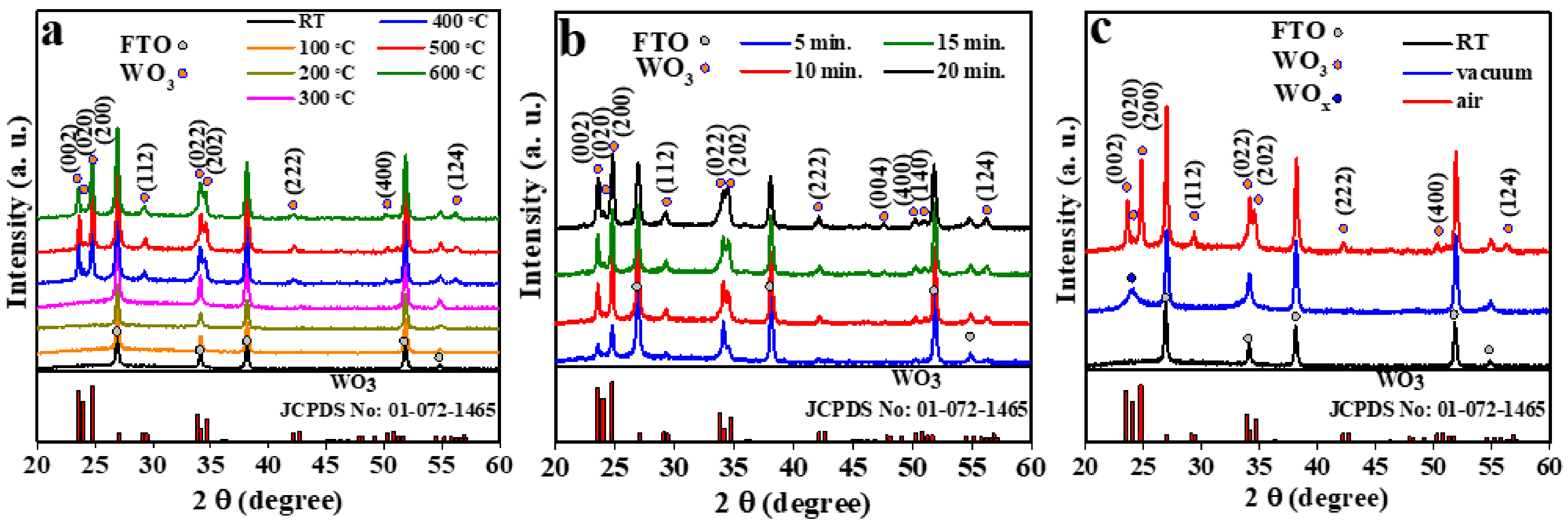
The structural evolution of WO3 as a function of annealing temperature, deposition time, and annealing environment was followed by X-ray diffraction (XRD). All the tested films were deposited on fluorine-doped tin oxide (FTO) substrate. Figure 1a shows the XRD patterns of the WO3 films annealed at different temperatures, starting from room temperature to 600 °C. It is clear that the as-deposited WO3 film as well as those annealed at 100, 200, and 300 °C have an amorphous structure, as they were no presence of any diffraction peak. The diffractions appeared at 26.8°, 34.1°, 38.1°, 51.8°, and 54.8° correspond to FTO [35]. When the annealing temperature is increased to 400 °C, the amorphous phase is discerned to transform into crystalline form. The diffractions recorded at 23.5°, 24.0°, 24.7°, 29.2°, 34.1°, 34.7°, 42.1°, 50.1°, and 56.2° are attributed to the crystalline phase of WO3. These diffractions correspond to (002), (020), (200), (112), (022), (202), (222), (400), and (124) reflections, respectively. The recorded diffractions are in good agreement with those reported for the WO3 monoclinic structure with P21/n space group (JCPDS No: 01-072-1465) [36,37]. A further increase in the calcination temperature from 400 °C to 600 °C did not show noticeable impact on the XRD of the films. The change in XRD patterns as a function of deposition time (or film thickness) is shown in Figure 1b. All the films grew in the same WO3 phase, and preferred orientation along (200) plane. The improvement in the diffraction intensity of the films deposited for 10 min and above, compared with 5 min deposited film, can be attributed to the enhancement in the crystallinity with the increase in film’s thickness. The crystallinity improvement in the thicker films can be related to the availability of favorable medium for the atoms’ thermal motion, which can lead to better alignment of crystallites [38]. A similar behavior was observed and reported for other metal oxides [39,40,41,42]. To investigate the impact of annealing environment, the films were also annealed in vacuum and air. Figure 1c compares the XRD patterns of the films obtained in vacuum and air by annealing at 500 °C. In case of the film annealed in vacuum showed a single, small, and broad diffraction at 23.9°, suggesting the formation of sub-stoichiometric form of WO3−x phase. This diffraction peak might be related to the (010) plane of the monoclinic Magnéli-Phase W18O49 which can be formed in oxygen-deficient annealing environment [43]. The weak crystallinity of WO3−x film might be attributed to the insufficient supply of oxygen atoms that can help in the growth of kinetically preferred orientation [44].
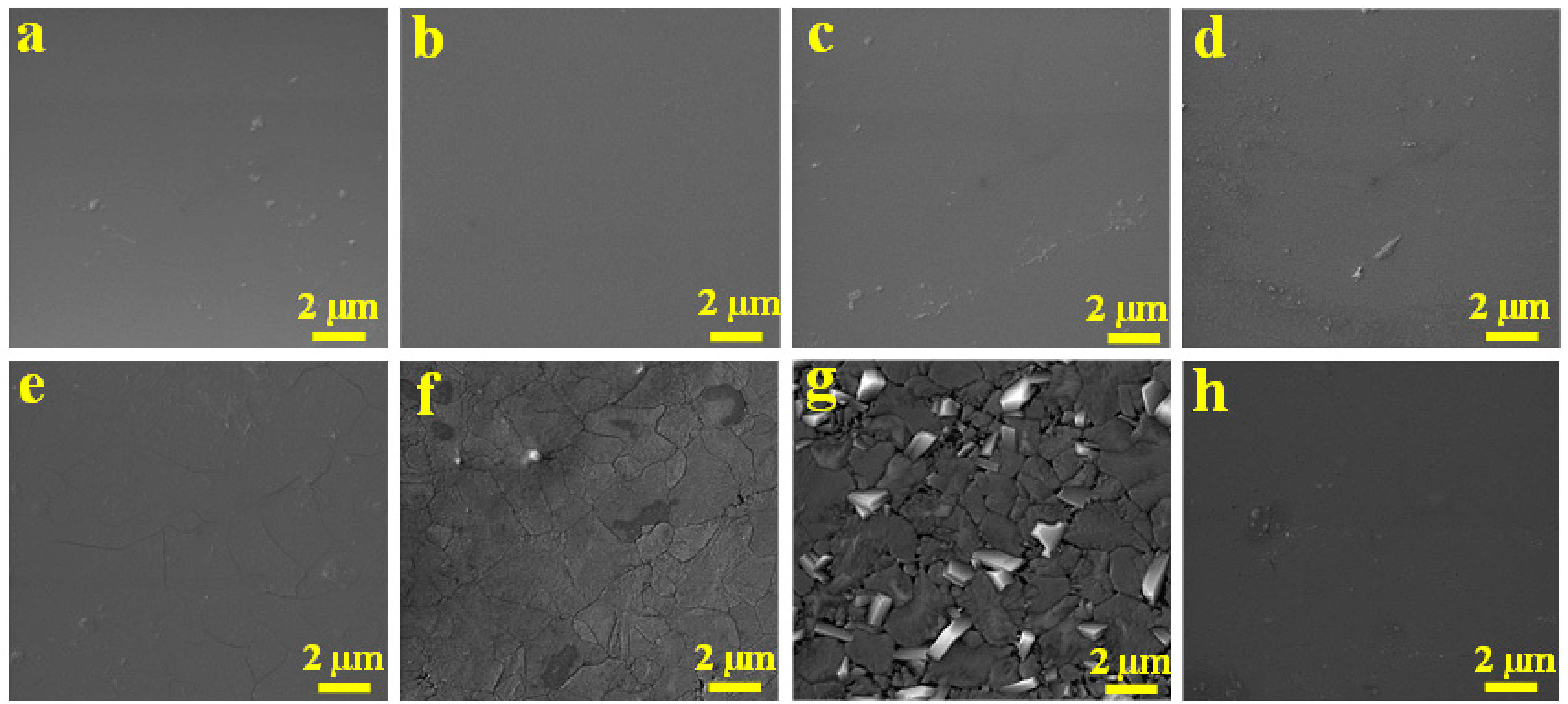
The information about the surface morphologies and the thickness of the WO3 thin films were obtained by field-emission scanning electron microscopy (FESEM). The qualities of the WO3 films collected after post-annealing at different temperatures in air are shown in Figure 2a–g. For comparison, the image of the WO3 films annealed at 500 °C in vacuum is shown in Figure 2h. The surfaces of the as-deposited and the films annealed at 100 °C, 200 °C, and 300 °C were dense, smooth, and crack-free, as shown in Figure 2a–d, respectively. The morphology change started with slight cracking for the film annealed at 400 °C (Figure 2e). These cracks might be due to the phase transition from the amorphous to the crystalline phase, as observed by the XRD. The cracks became more prominent for the film annealed at 500 °C as the tungsten oxide particles began to agglomerate (Figure 2f). With further increase in the heating temperature to 600 °C, the cracks increased significantly. The tungsten oxide particle aggregation increased to form a continuous sheet, as shown in Figure 2g. The surface of the WO3 film post-annealed at 500 °C in vacuum is smooth with fewer cracks as compared to its counterpart film annealed in air at the same temperature (Figure 2h).
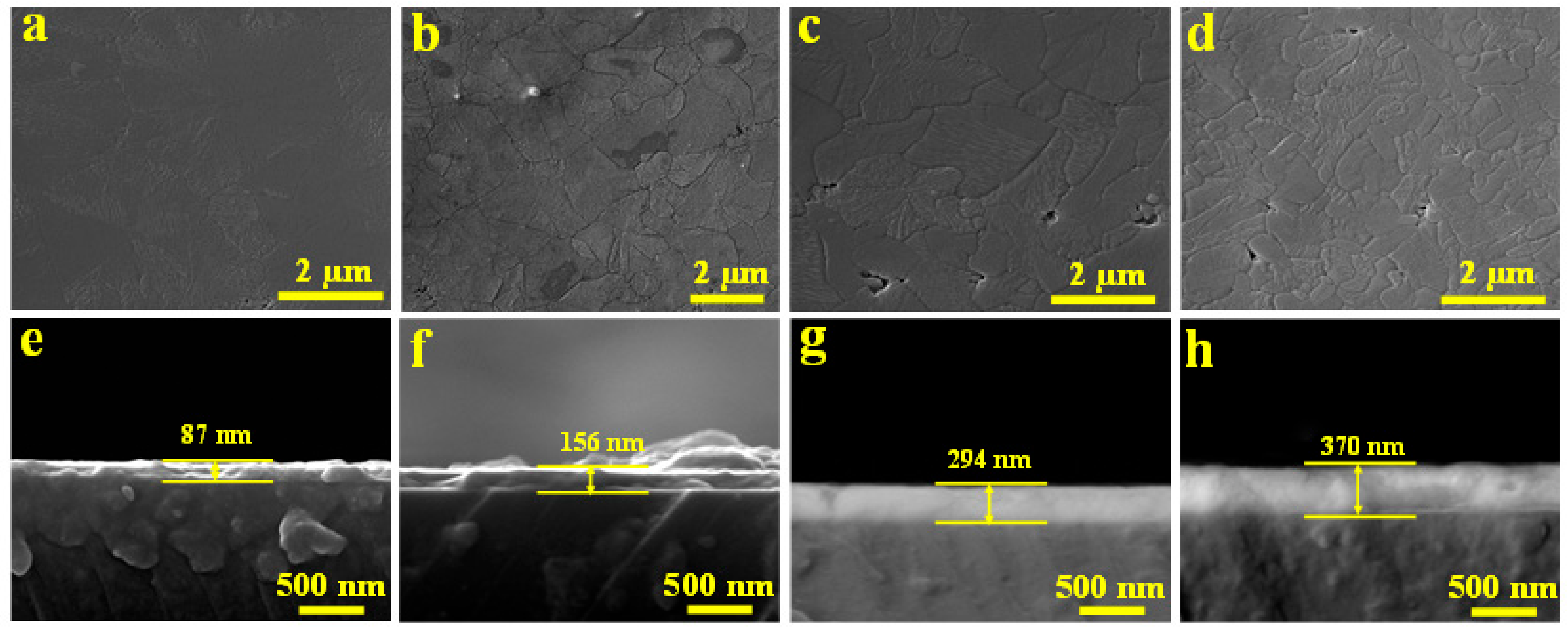
The surface and the thickness of the WO3 films obtained after different disposition time, annealed at 500 °C in air, are obtained by top-view and cross-section of FESEM images, as shown in Figure 3. The WO3 film deposited for 5 min shows a dense, rough texture and void-free morphology with a thickness of ~87 nm (Figure 3a,e). When the deposition time was increased to 10 min, a few cracks appeared on the film’s surface as a result of thermal aggregation [35], and the film thickness was calculated to be ~156 nm (Figure 3b,f). More cracks and voids appeared with increasing the deposition time to 15 and 20 min (Figure 3c,d). The WO3 film thickness increased to ~294 and ~370 nm (Figure 3g,h), respectively. The obtained results suggest that the evolution of the surface morphology of the WO3 films was dependent on its deposition time or thickness. A similar conclusion was mentioned in previous studies [45,46,47]. It is worth noting that the evolution of the film’s thickness was almost linear with the deposition time.
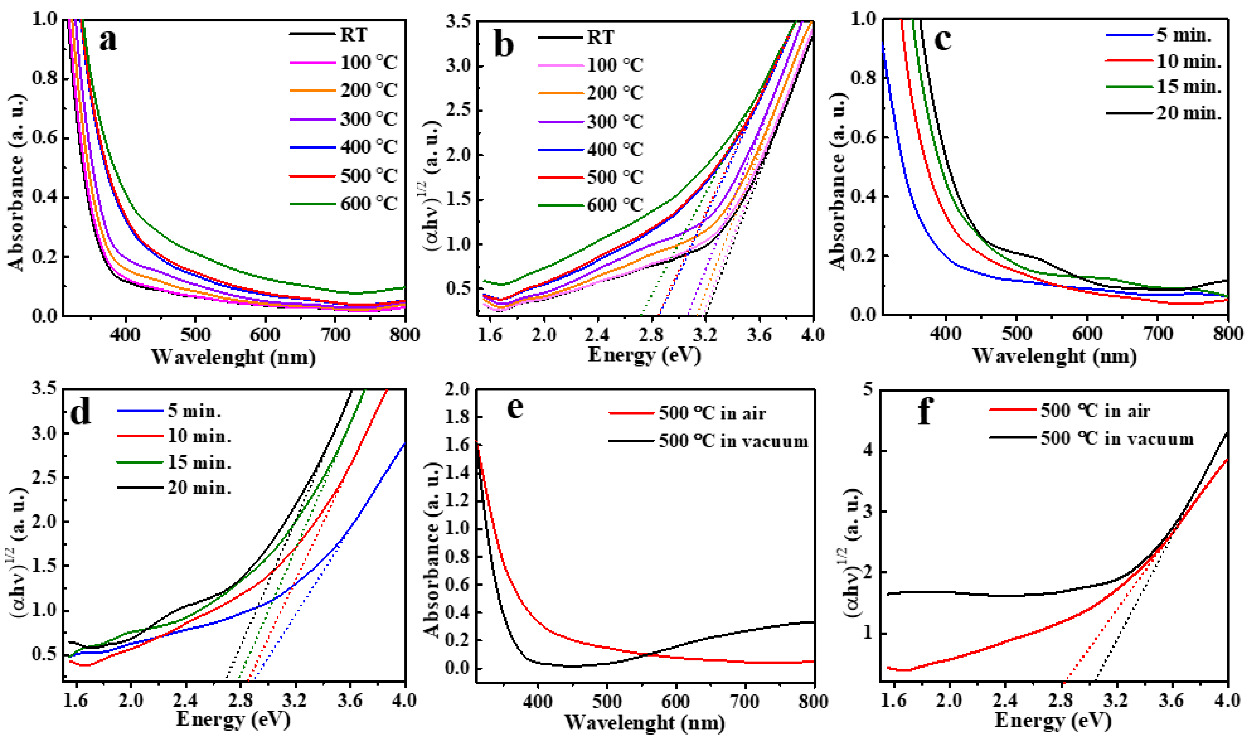
The optical properties of the WO3 thin films were investigated by ultraviolet-visible (UV-Vis) absorption spectroscopy in the wavelength range from 800 to 200 nm. The recorded spectra are shown in Figure 4. Figure 4a shows the UV-Vis absorption spectra of WO3 films annealed at different temperatures between 100 and 600 °C in air. The absorption spectra can be seen shifting to the shorter wavelength region as the post-annealing temperature increased to 600 °C. The increase in the absorption spectra in the visible region for the films that annealed at elevated temperature (400–600 °C) might be due to the increase in the scattered light caused by the increase in the grain size and surface roughness, as confirmed by the FESEM findings [48,49]. The shift in the fundamental absorption edge toward a longer wavelength can be explained by investigating the features of the optical bandgap of the fabricated films using Tauc’s relation [50,51]:
where (α) is the absorption coefficient, (h) is the Planck’s constant, (ν) is the frequency, (A) is constant, (Eg) is the optical bandgap, (n) is constant (= 2 for direct bandgap, = 1⁄2 for indirect bandgap).
(αhν)n = A(hν − Eg)
Figure 4b shows the functional dependence of (αhν)(1/2) versus the absorbed photon energy. The optical bandgap of WO3 films can be estimated by extrapolating the liner part of (αhν)(1/2) curves to zero [51]. The optical bandgap of WO3 films decreased, from 3.2 eV for the as-deposited film to 2.7 eV for 600 °C annealed film, with the increase in the post-annealing temperature. This behavior can be attributed to the presence of thermal-induced defects [52]. Annealing at a high temperature can affect the nanostructure of WO3 by introducing oxygen vacancies. These vacancies create sublevels between the conduction and valance band of the WO3 band structure, and hence decreasing its bandgap [53]. The influence of WO3 film’s thickness on UV-Vis light absorption was also investigated, as shown in Figure 4c. The absorption spectra, below 600 nm, was significantly increased by the increase of the deposition time, presumably due to particle size growth caused by the rise in the WO3 mass thickness. The bandgap of the WO3 films was found to be decreased with increasing the deposition time. The WO3 film deposited for 5 min showed the highest bandgap (2.9 eV) due to the quantum size confinement [47]. The bandgap decreased gradually to reach the lowest value (2.7 eV) for the film deposited for 20 min due to the size change from one dimension to the bulk material. The annealing atmosphere was also found to have an impact on the UV-Vis absorbance spectra and optical bandgap of the films, Figure 4e,f, respectively. The film annealed in air exhibited a smaller light absorption at a higher wavelength (visible range) due to the formation of fully stoichiometric WO3−x film (Figure 4e) [47,54]. The vacuum-annealed film showed a higher bandgap (3.05 eV) compared to air-annealed film (2.8 eV) (Figure 4f); this might be due to the formation of non-stoichiometric tungsten oxide phase (WO3−x). The formation of WO3−x is discussed in the X-ray photoelectron spectroscopy (XPS) results.
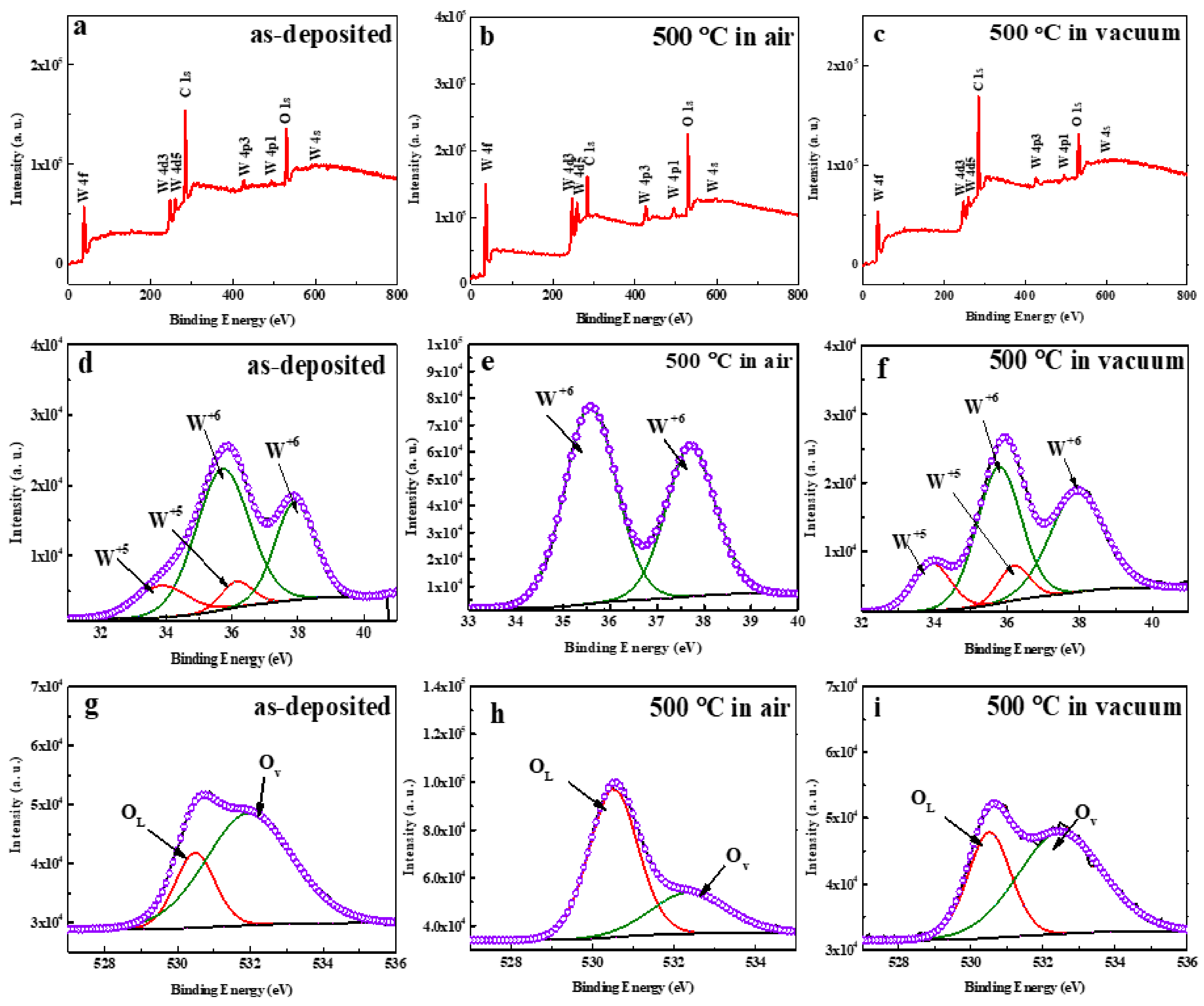
The compositional analysis of WO3 films was performed using X-ray photoelectron spectroscopy (XPS), and the data is presented in Figure 5. Figure 5a–c show the XPS survey spectra of as-deposited, air-annealed, and vacuum-annealed (at 500 °C) WO3 films. All the survey scan spectra confirm the presence of W and O without any impurities. Figure 5d–f demonstrate the deconvoluted peaks of W 4f spectra for the as-deposited WO3 and WO3 films annealed at 500 °C in air and vacuum, respectively. The deconvolution of high resolution XPS spectra of W 4f in as-deposited film shows two chemical binding energies of two different oxidation state; W+5 (at 33.9 eV (W 4f7/2) and 36.2 eV (W 4f5/2), and W+6 (at 35.7 eV (W 4f7/2) and 37.9 eV (W 4f5/2) [55,56] (Figure 4d). The presence of W+5 oxidation state reflects the existence of crystal defects in the form of oxygen vacancies [57]. On the other side, the high-resolution XPS spectrum of air-annealed WO3 film shows only one binding energy spectrum, at 35.6 eV (W 4f7/2) and 37.8 eV (W 4f5/2), which is related to W+6 oxidation state (Figure 5e). This confirms the formation of fully oxidized WO3 film as a result of post-annealing treatment in the air. For the vacuum-annealed film (Figure 5f), both binding energy spectra (oxidation states) of W+5 and W+6 were found at 33.8 eV (W 4f7/2), 36.2 eV (W 4f5/2), 35.8 eV (W 4f7/2) and 37.9 eV (W 4f5/2), respectively. This was caused by the absence of oxygen in the ambient annealing atmosphere. Figure 5g–i show the deconvoluted peaks of O 1s spectra for the as-deposited WO3 and WO3 films annealed at 500 °C in air and vacuum, respectively. The high-resolution XPS spectrum of the O 1s for the as-deposited film was deconvoluted into two binding energies; one at 530.4 eV, which corresponds to lattice oxygen (OL), and the other at 532.1 eV, which is due to the oxygen vacancy (Ov) (Figure 5g) [58,59]. After the air-annealing treatment (Figure 5h), it was observed that the number of oxygen vacancies reduced compared to the as-deposited film as a result of filling the vacancies by the absorbed oxygen from the ambient atmosphere [57]. The amount of oxygen vacancy in the vacuum-annealed film had not significantly changed due to the lack of oxygen molecules in this annealing atmosphere (Figure 5i).
DFT calculations were performed to evaluate the theoretical bandgap and density of state (DOS) of the WO3 photoanode using a similar phase structure. Figure 6a shows the optimized geometry of the monoclinic WO3 structure. The electronic band structure and its projected density of state of WO3, calculated by using the generalized gradient approximation GGA-PBE exchange-correlation function, are shown in Figure 6b. The bandgap of WO3 was calculated to be around 1.14 eV, which is very small compared to the experimental value. This is a common problem with the GGA functional, which strictly underestimates the bandgap calculations [60]. The DOS shows that the conduction band (CB) of WO3 is mainly associated with W_5d orbitals, while O_2p orbitals dominate the valance band (VB). The bandgap calculation was improved by introducing the hybrid DFT calculation using B3YLP functional as presented in Figure 6c. It was found that the calculated bandgap was improved to 2.61 eV (indirect bandgap), which is closed to the experimental value estimated in this article.
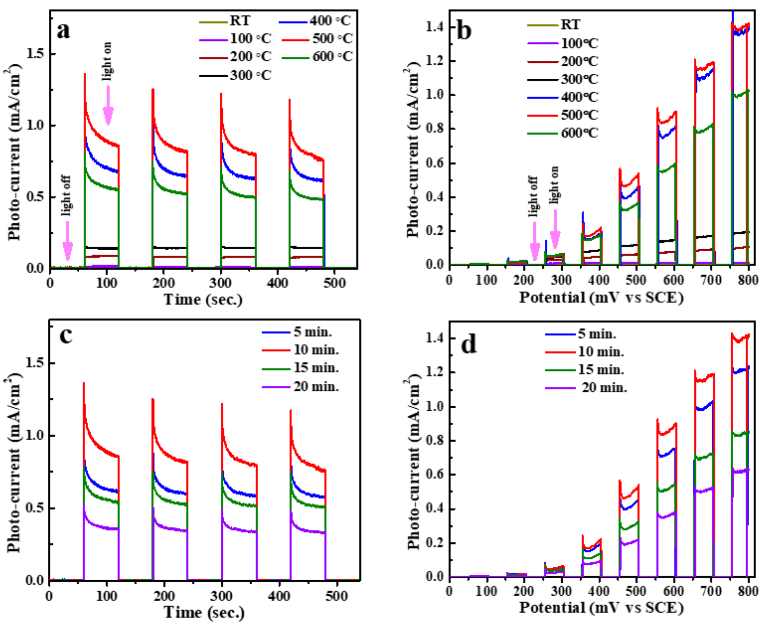
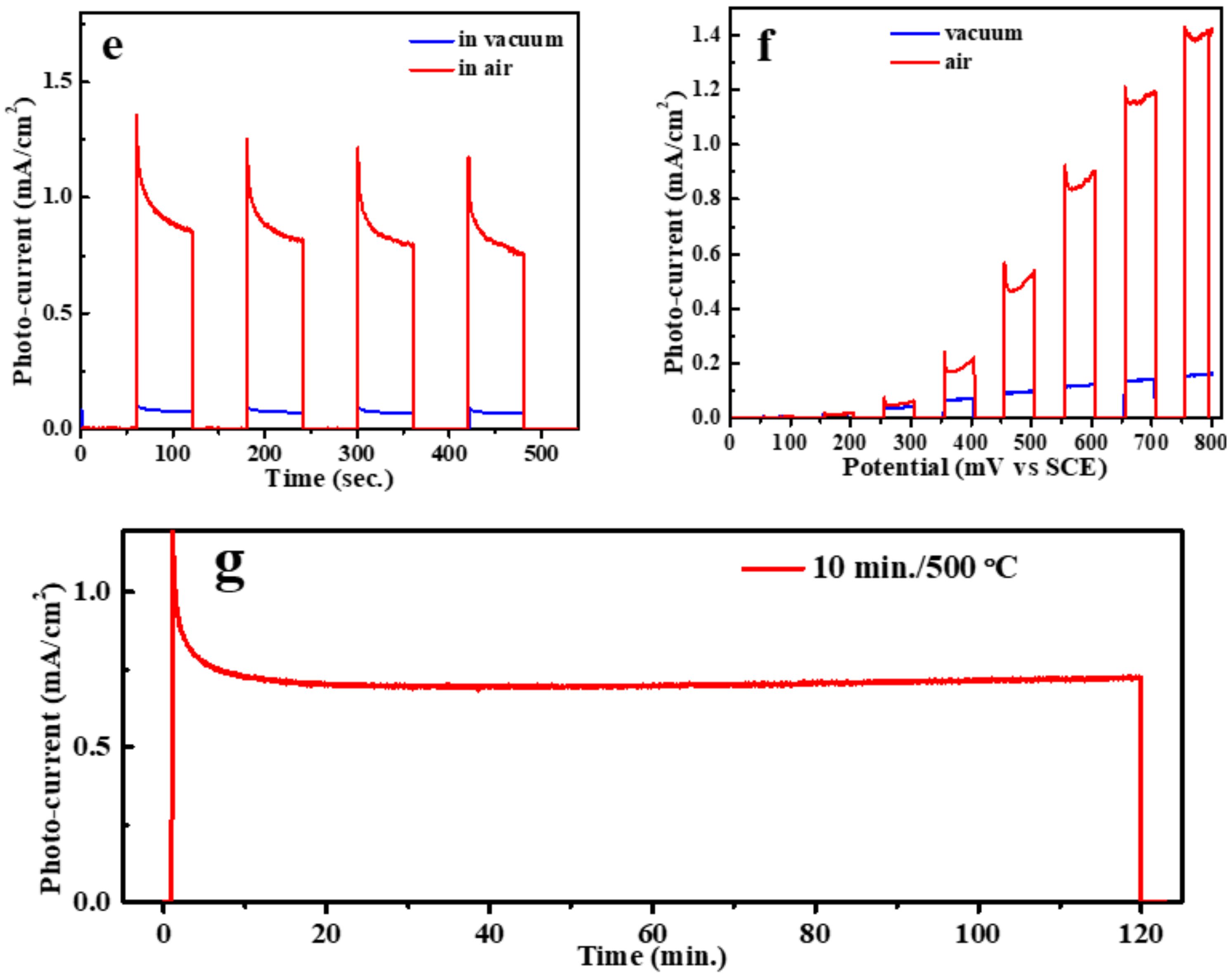
The PEC performance of the WO3 films obtained under different conditions was evaluated under illumination using chronoamperometry and linear sweep voltammetry tests. All the PEC measurements were carried out in 0.1 M Na2SO4 aqueous electrolyte. The generation of photocurrent density as a function of time was investigated using a light on/off chronoamperometry test. The results for the WO3 films obtained after annealing at different temperatures are shown in Figure 7a. The measurement was performed at 600 mV vs saturated calomel electrode (SCE). The electrodes did not show any noticeable photocurrent when the light source was switched-off (~zero dark current). Meanwhile, an instantaneous current density was generated under illumination, indicating the photocatalytic behavior of the electrodes. It can be seen that the generated photocurrent density produced by these electrodes were dependent on their post-annealing temperature. For example, as-deposited film and films annealed at 100–300 °C showed a weak photocurrent (less than 0.2 mA/cm2). However, a dramatic improvement in the photocurrent was observed for the films annealed at 400–600 °C. The films obtained after heat treatment at 400, 500, and 600 °C produced 0.6, 0.9, and 0.7 mA/cm2, respectively. This improvement can be rationalized in terms of electrical conductivity, which is likely to increase with the phase transition of WO3 from amorphous to crystalline, as confirmed by the XRD [61]. In addition, it can be correlated to the films’ bandgap; a smaller bandgap can absorb more light, and hence more electron/hole pairs can be generated. Although WO3 film annealed at 600 °C has a smaller bandgap than the film obtained at 500 °C, the large number of cracks present in the former film can affect its surface continuity, which in turn can decrease its conductivity. Linear sweep voltammetry (I–V) curves of WO3 films, annealed at a different temperature, were obtained in the range of 0–800 mV vs SCE (Figure 7b). The I–V curves showed that the photocurrent of these electrodes increases with the increase in forward potentials under illumination, which agrees with the n-type semiconductor [62,63]. Besides, all the electrode films did not generate any dark current at higher potential (800 mV), indicating a complete photo-responsive behavior. The effect of deposition time on the PEC performance was also investigated, and the results are shown in Figure 7c). The maximum photocurrent (0.9 mA/cm2) was recorded with the film deposited for 10 min, followed by the films deposited for 5 min (0.7 mA/cm2) 15 min (0.6 mA/cm2), and 20 min (0.4 mA/cm2). As determined by the FESEM, the respective thickness of the films deposited for 5, 10, 15, and 20 min are 87 nm, 156 nm, 294 nm, and 2370 nm. The film’s thickness can have significant impact on electrical conductivity and charge transfer resistance [38]. Therefore, a thinner film might have many grain boundaries that can increase the scattered charge carriers [38]. On the other hand, the thicker film’s resistance can also be increased due to the increase in the charge’s diffusion path [64]. Similar photocatalytic behavior was observed in the current-potential (I–V) curves for all thicknesses (Figure 7d). The annealing atmosphere found to have a substantial effect on the PEC activity of the WO3 films (Figure 7e). A smaller photocurrent (0.1 mA/cm2) was generated from the vacuum-annealed film; this might be due to its high resistivity (low crystallinity), or due to the formation of non-photo-active phase (WO3−x). The PEC activity of the vacuum-annealed film remains low even at high potential; 0.2 mA/cm2 at 800 mV vs SCE (Figure 7f). The stability of the photoanodes is important metric. The WO3 film prepared after 10 min deposition time followed by annealing at 500 °C in air was selected to evaluate the photoelectrochemical stability. The current-time curve recorded at a potential of 600 mV for 120 min is shown in Figure 7g. The photoelectrode showed an instantaneous generation of photocurrent when the light was turned on, followed by a slight decrease during the first 20 min, presumably as a result of electrical double layer capacitance i.e., accumulation of charge carriers at the electrolyte/film interface. After 20 min, the photoelectrode exhibited highly stable photocurrent generation, and the photocurrent remains stable at ~0.75 mA/cm2 for 100 min. After 100 min, the photocurrent decreased sharply when the light was turned off. This suggests that the recorded photocurrent was the result of photoexcitation of the WO3 and water oxidation reaction in the presence of light.
The PEC activity of the as-prepared WO3 photoelectrode, which was prepared with 10 min deposition followed by annealing at 500 °C, was compared with those recently reported in the literature. The photocurrent and important conditions are presented in the Table 1. As can be seen, the as-prepared WO3 photoelectrode compares favorably with other photoelectrodes.
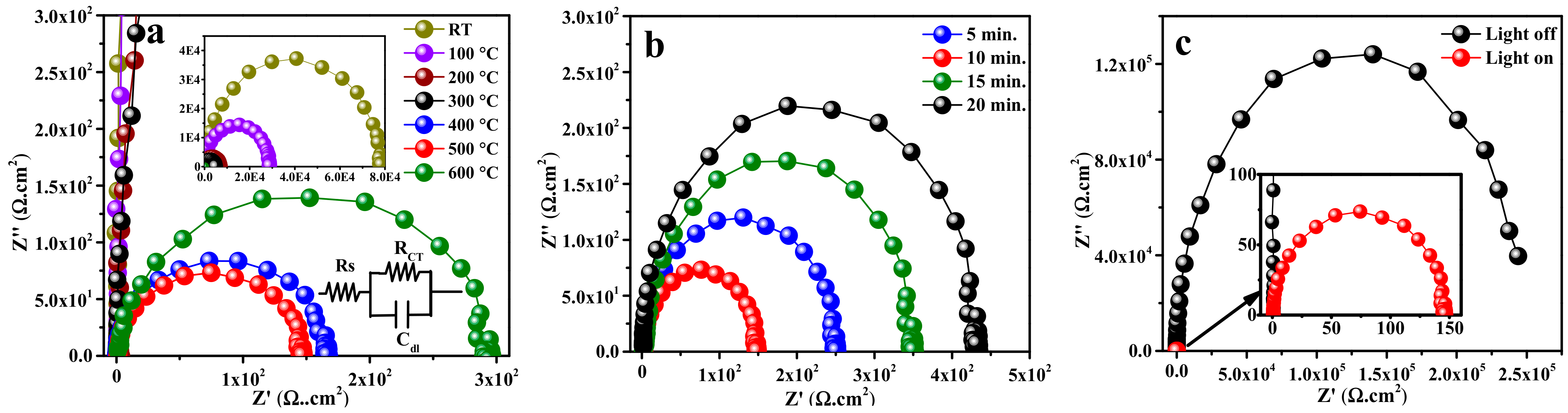
Electrochemical impedance spectroscopy (EIS) measurements were performed to study the resistivity and charge transfer process of the WO3 films. The measurements were performed in the frequency range of 10−2–1 mHz. The Nyquist plots (imaginary vs real impedance) of as-deposited and annealed (100–600 °C) WO3 films are shown in Figure 8a. The results were obtained in presence of light. All the impedance data was fitted with a randle circuit, which consists of a charge transfer resistance (Rct) that is connected with a capacitor in parallel and solution resistance (Rs) in series [75]. It can be observed that the charge transfer resistance of the films annealed at 400 °C and above are significantly smaller (Rct = 147, 166, and 289 Ω for 500, 400, and 600 °C, respectively) as compared to the films annealed at 300 °C and below (Rct = 4.7, 7.1, 28.6, and 77.5 KΩ for 300, 200, 100 °C, and room temperature). These findings are in good agreement with XRD and PEC results; the crystalline WO3 films showed lower resistance and higher photocatalytic activity than amorphous films. The Nyquist plots of the WO3 films, annealed at 500 °C in air, obtained with different deposition time (or film thickness) are shown in Figure 8b. The Rct of the films deposited for 5, 10, 15, and 20 min are calculated to ~250, ~147, ~348, and ~433 Ω, respectively. An optimal film’s thickness is required to avoid electron scattering at the grain boundaries in thinner films and electron/hole pair recombination in the thicker films. To highlight the effect of light on conductivity, the Nyquist plots of the WO3 film (deposition time = 10 min, annealing temperature = 500 °C) were recorded under light and dark conditions. The results are compared in the Figure 8c. As evident, a huge charge transfer resistance (Rct = 250 kΩ) is registered in the absence of light, explaining the negligible dark current noticed during on/off chronoamperometry measurements.
3. Experimental Details
3.1. Synthesis of WO3 Thin Films
The preparation of the WO3 thin films was carried out using a DC reactive sputtering system (model NSC-4000, Nanomaster, Austin, TX, USA). A circular disk made from 99.995% of W (purchased from ACI alloys INC, San Jose, CA, USA) was used as the sputtering target. A conductive coated glass (FTO) was utilized as a substrate for the deposition of WO3 films. In order to study the effect of post-annealing temperature on the PEC performance, FTO substrates were cleaned, dried, and placed inside the sputtering chamber. The sputtering chamber was evacuated to an initial pressure of 8 × 10⁻⁶ torr. The deposition process was performed at 100 watts in a 70 sccm mixture of argon and oxygen (1:1) atmosphere with a working pressure of 3 × 10⁻³ torr. The deposited films were then post-annealed in air or vacuum at different temperature for 2 h, and the substrate heater was sealed in an evacuated chamber. The thickness of the WO3 films was controlled by changing the deposition time (5, 10, 15, 20 min) while keeping the other deposition parameters constant.
3.2. WO3 Films Characterization
Various techniques were used to characterize the fabricated WO3 films. X-ray diffraction (XRD, Rigaku Miniflex 600 X-ray Diffraction, Tokyo, Japan, with Cu K irradiation at λ = 1.5406 Å) was used to obtain the phase and structure information of the photoanode films. Felid emission scanning microscopy (FESEM Tescan Lyra-3, Brno-Kohoutovice, Czech Republic) was used to study the surface morphology (top view image) and film’s thickness (cross-section image) of the deposited films. A double-beam UV-Vis spectrometer (Jasco V-570, Tokyo, Japan) was used to observe the optical absorption spectra. X-ray photoelectron spectroscopy (XPS, Model: ESCALAB250Xi, Thermo Fisher, Waltham, MA, USA) was used to examine the films’ surface composition.
3.3. Theoretical Calculation
Density functional theory (DFT) and pseudopotential methods were carried out to obtain the first principle band structure and density of state (DOS) calculations of WO3 using Vienna ab initio simulation (VASP) package. Generalized gradient approximation (GGA) along with the Perdew−Burke−Ernzerhof (PBE) exchange-correlation functional was used to find the standard band structure and DOS of WO3. 630 eV was set as an energy cut-off for a basis set. The k-mesh of Monkhorst−Pack scheme was used to simplify the Brillouin zone for bulk WO3. A value of 10−6 eV per atom was used as self-consistent field (SCF) tolerance. Hybrid functional DFT calculation using B3YLP correction functional was used to get an accurate band gap value.
3.4. Photoelectrochemical (PEC) Study
The photoelectrocatalytic performance measurements; chronoamperometry, liner sweep voltammetry, and electrochemical impedance spectroscopy of the WO3 photoanodes was studied in a quartz cell attached to a potentiostat (Voltalab, model: PGZ 402, Colorado, USA) with a three-electrode measurement system. WO3 films, saturated calomel electrode (SCE), and platinum coil were used as working electrodes, reference electrode, and counter electrode, respectively. A 0.1 M aqueous sodium sulfate (Na2SO4) solution was used as an electrolyte. A 300 watt Xenon lamp (Model: Max-303, Tokyo, Japan) was used as an illumination source with a wavelength () range of 300 to 600 nm and 100 mW cm−2 light intensity. The charge transfer resistance (Rct) of the deposited films was evaluated under dark and light using electrochemical impedance spectroscopy (EIS).
4. Conclusions
In conclusion, this study demonstrated that the important properties of WO3 thin films can be fine-tuned by controlling deposition time, and post-annealing temperature and environment. The band gap of WO3 can be controlled between 3.2 and 2.7 eV by adjusting the post-annealing temperature between 100 and 600 °C. It is discerned that the photoelectrocatalytic activity of WO3 photoelectrodes increased with decreasing bandgap, and the maximum photocurrent (0.9 mA/cm2 at 0.6 VSCE) was recorded with WO3 thin film heated at 500 °C with a bandgap of 2.85 eV. The annealing environment is also found to have significant impact on the performance—the WO3 film heated under air exhibited much better photoelectrochemical water oxidation than that of annealed under inert (argon) atmosphere. In addition to the annealing temperature and environment, the film thickness is another crucial feature that dictated the performance of WO3. The thickness of WO3 film can be easily controlled between ~85 and ~370 nm within a short deposition time ranging from 5 to 20 min, and the maximum photocurrent was observed when the film thickness was approximately 150 nm. The charge transfer resistance of the films annealed at 400 °C and above was significantly smaller as compared to the films annealed at 300 °C and below, which was in good agreement with the PEC trend where the crystalline WO3 films showed higher photoelectrocatalytic activity than the amorphous films. In addition, the WO3 photoelectrode exhibited excellent photoelectrochemical stability—the electrode was stable for the entire measurement time (120 min).
Author Contributions
Conceptualization, A.K.M., Q.A.D. and M.Q.; Formal analysis, Z.H.Y.; Investigation, A.K.M., Q.A.D. and Z.H.Y.; Methodology, A.K.M., Q.A.D. and M.Q.; Supervision, Z.H.Y.; Writing original draft, A.K.M.; Review & editing, M.Q., Q.A.D. and Z.H.Y. All authors have read and agreed to the published version of the manuscript.
Funding
This research was funded by the Deanship of Scientific Research (DSR) and the King Abdullah City for Atomic and Renewable Energy (K.A.CARE) Energy Research & Innovation Center at King Fahd University of Petroleum & Minerals (KFUPM).
Data Availability Statement
The data presented in this study are available on request from the corresponding author.
Acknowledgments
The authors would like to acknowledge the support provided by the Deanship of Scientific Research (DSR) at King Fahd University of Petroleum & Minerals (KFUPM) for funding this work. M. Qamar acknowledges the funding support provided by the King Abdullah City for Atomic and Renewable Energy (K.A.CARE).
Conflicts of Interest
The authors declare no conflict of interest.
References
- Medisetty, V.M.; Kumar, R.; Ahmadi, M.H.; Vo, D.-V.N.; Ochoa, A.A.V.; Solanki, R. Overview on the Current Status of Hydrogen Energy Research and Development in India. Chem. Eng. Technol. 2020, 43, 613–624. [Google Scholar] [CrossRef]
- Sami, B.S. A Survey of Hydrogen Energy and I-Energy Applications: Household Intelligent Electrical Power Systems. IEEE Access 2020, 8, 55181–55203. [Google Scholar] [CrossRef]
- Akal, D.; Öztuna, S.; Büyükakın, M.K. A review of hydrogen usage in internal combustion engines (gasoline-Lpg-diesel) from combustion performance aspect. Int. J. Hydrog. Energy 2020, 45, 35257–35268. [Google Scholar] [CrossRef]
- Hu, G.-L.; Lei, Y.-J.; Hu, R.; Sun, H.-M.; Gu, Q.; Ren, D.-Z.; Wang, H.-Y. Photo-electrocatalytic water oxidation based on an earth-abundant metallic semiconductor-molecule hybrid photoanode. Int. J. Hydrog. Energy 2019, 44, 31884–31891. [Google Scholar] [CrossRef]
- Idriss, H. Hydrogen production from water: Past and present. Curr. Opin. Chem. Eng. 2020, 29, 74–82. [Google Scholar] [CrossRef]
- Idriss, H. Toward Large-Scale Hydrogen Production from Water: What Have We Learned and What Are the Main Research Hurdles to Cross for Commercialization? Energy Technol. 2021, 9, 2000843. [Google Scholar] [CrossRef]
- Fujishima, A.; Honda, K. Electrochemical Photolysis of Water at a Semiconductor Electrode. Nat. Cell Biol. 1972, 238, 37–38. [Google Scholar] [CrossRef] [PubMed]
- Kudo, A.; Miseki, Y. Heterogeneous photocatalyst materials for water splitting. Chem. Soc. Rev. 2009, 38, 253–278. [Google Scholar] [CrossRef] [PubMed]
- Narayanan, N.; Deepak, N. Enhancement of visible luminescence and photocatalytic activity of ZnO thin films via Cu doping. Optik 2018, 158, 1313–1326. [Google Scholar] [CrossRef]
- Jiang, C.; Moniz, S.J.A.; Junwang, T.; Zhang, T.; Tang, J. Photoelectrochemical devices for solar water splitting—Materials and challenges. Chem. Soc. Rev. 2017, 46, 4645–4660. [Google Scholar] [CrossRef] [Green Version]
- Saraswat, S.K.; Rodene, D.D.; Gupta, R.B. Recent advancements in semiconductor materials for photoelectrochemical water splitting for hydrogen production using visible light. Renew. Sustain. Energy Rev. 2018, 89, 228–248. [Google Scholar] [CrossRef]
- Yang, Y.; Niu, S.; Han, D.; Liu, T.; Wang, G.; Li, Y. Progress in Developing Metal Oxide Nanomaterials for Photoelectrochemical Water Splitting. Adv. Energy Mater. 2017, 7, 1700555. [Google Scholar] [CrossRef]
- Ahmed, M.; Adam, A.; Khan, A.; Siddiqui, M.; Yamani, Z.; Qamar, M. Synthesis of mesoporous NiWO4 nanocrystals for enhanced photoelectrochemical water oxidation. Mater. Lett. 2016, 177, 135–138. [Google Scholar] [CrossRef]
- Jeon, T.H.; Monllor-Satoca, D.; Moon, G.; Kim, W.; Kim, H.; Bahnemann, D.W.; Park, H.; Choi, W. Ag(I) ions working as a hole-transfer mediator in photoelectrocatalytic water oxidation on WO3 film. Nat. Commun. 2020, 11, 1–9. [Google Scholar] [CrossRef] [PubMed] [Green Version]
- Shen, X.; Yao, M.; Sun, K.; Zhao, T.; He, Y.; Chi, C.-Y.; Zhou, C.; Dapkus, P.D.; Lewis, N.S.; Hu, S. Defect-Tolerant TiO2-Coated and Discretized Photoanodes for >600 h of Stable Photoelectrochemical Water Oxidation. ACS Energy Lett. 2021, 6, 193–200. [Google Scholar] [CrossRef]
- Chatterjee, S.; Bhanja, P.; Ghosh, D.; Kumar, P.; Das, S.K.; Dalapati, S.; Bhaumik, A. Metformin-Templated Nanoporous ZnO and Covalent Organic Framework Heterojunction Photoanode for Photoelectrochemical Water Oxidation. ChemSusChem 2021, 14, 408–416. [Google Scholar] [CrossRef]
- Kaur, G.; Divya; Khan, S.A.; Satsangi, V.R.; Dass, S.; Shrivastav, R. Expanded light-absorption and efficient charge-separation: Bilayered thin film nano-hetero-structures, CuO/Cu–ZnO, make efficient photoanode in photoelectrochemical water splitting. J. Appl. Electrochem. 2020, 50, 887–906. [Google Scholar] [CrossRef]
- Ko, T.-R.; Chueh, Y.-C.; Lai, Y.-H.; Lin, C.-Y. Simultaneous enhancement in charge separation and interfacial charge transfer of BiVO4 photoanode for photoelectrochemical water oxidation. J. Taiwan Inst. Chem. Eng. 2020, 111, 80–89. [Google Scholar] [CrossRef]
- Yuan, J.-T.; Wang, Z.; Wang, L.; Liu, R.-J. Preparation, Surface Modification, and Characteristic of α-Fe2O3 Nanoparticles. J. Nanosci. Nanotechnol. 2020, 20, 3031–3037. [Google Scholar] [CrossRef] [PubMed]
- Dutta, V.; Sharma, S.; Raizada, P.; Thakur, V.K.; Khan, A.A.P.; Saini, V.; Asiri, A.M.; Singh, P. An overview on WO3 based photocatalyst for environmental remediation. J. Environ. Chem. Eng. 2021, 9, 105018. [Google Scholar] [CrossRef]
- Liu, J.; Zhang, G.; Guo, K.; Guo, D.; Shi, M.; Ning, H.; Qiu, T.; Chen, J.; Fu, X.; Yao, R.; et al. Effect of the Ammonium Tungsten Precursor Solution with the Modification of Glycerol on Wide Band Gap WO3 Thin Film and Its Electrochromic Properties. Micromachines 2020, 11, 311. [Google Scholar] [CrossRef] [Green Version]
- Gu, Y.; Zheng, W.; Bu, Y. Facile preparation of nanoflower structured WO3 thin film on etched titanium substrate with high photoelectrochemical performance. J. Electroanal. Chem. 2019, 833, 54–62. [Google Scholar] [CrossRef]
- Yun, G.; Balamurugan, M.; Kim, H.-S.; Ahn, K.-S.; Kang, S.H. Role of WO3 Layers Electrodeposited on SnO2 Inverse Opal Skeletons in Photoelectrochemical Water Splitting. J. Phys. Chem. C 2016, 120, 5906–5915. [Google Scholar] [CrossRef]
- Bertus, L.; Duta, A. Synthesis of WO3 thin films by surfactant mediated spray pyrolysis. Ceram. Int. 2012, 38, 2873–2882. [Google Scholar] [CrossRef]
- Han, J.; Ko, K.-W.; Sarwar, S.; Lee, M.-S.; Park, S.; Hong, S.; Han, C.-H. Enhanced electrochromic properties of TiO2 nanocrystal embedded amorphous WO3 films. Electrochim. Acta 2018, 278, 396–404. [Google Scholar] [CrossRef]
- Olejníček, J.; Brunclíková, M.; Kment, Š.; Hubička, Z.; Kmentová, H.; Kšírová, P.; Čada, M.; Zlámal, M.; Krýsa, J. WO 3 thin films prepared by sedimentation and plasma sputtering. Chem. Eng. J. 2017, 318, 281–288. [Google Scholar] [CrossRef]
- Qamar, M.; Drmosh, Q.; Ahmed, M.I.; Qamaruddin, M.; Yamani, Z.H. Enhanced photoelectrochemical and photocatalytic activity of WO3-surface modified TiO2 thin film. Nanoscale Res. Lett. 2015, 10, 54. [Google Scholar] [CrossRef] [Green Version]
- Vidyarthi, V.S.; Hofmann, M.; Savan, A.; Sliozberg, K.; König, D.; Beranek, R.; Schuhmann, W.; Ludwig, A. Enhanced photoelectrochemical properties of WO3 thin films fabricated by reactive magnetron sputtering. Int. J. Hydrog. Energy 2011, 36, 4724–4731. [Google Scholar] [CrossRef]
- Cole, B.; Marsen, B.; Miller, E.; Yan, Y.; To, B.; Jones, K.; Al-Jassim, M. Evaluation of Nitrogen Doping of Tungsten Oxide for Photoelectrochemical Water Splitting. J. Phys. Chem. C 2008, 112, 5213–5220. [Google Scholar] [CrossRef]
- Marsen, B.; Miller, E.L.; Paluselli, D.; Rocheleau, R.E. Progress in sputtered tungsten trioxide for photoelectrode applications. Int. J. Hydrog. Energy 2007, 32, 3110–3115. [Google Scholar] [CrossRef]
- Fendrich, M.; Popat, Y.; Orlandi, M.; Quaranta, A.; Miotello, A. Pulsed laser deposition of nanostructured tungsten oxide films: A catalyst for water remediation with concentrated sunlight. Mater. Sci. Semicond. Process. 2020, 119, 105237. [Google Scholar] [CrossRef]
- Mohamed, A.M.; Shaban, S.A.; El Sayed, H.A.; Alanadouli, B.E.; Allam, N.K. Morphology–photoactivity relationship: WO 3 nanostructured films for solar hydrogen production. Int. J. Hydrog. Energy 2016, 41, 866–872. [Google Scholar] [CrossRef]
- Han, H.S.; Park, W.; Hwang, S.W.; Kim, H.; Sim, Y.; Surendran, S.; Sim, U.; Cho, I.S. (0 2 0)-Textured tungsten trioxide nanostructure with enhanced photoelectrochemical activity. J. Catal. 2020, 389, 328–336. [Google Scholar] [CrossRef]
- Fang, Y.; Lee, W.C.; Canciani, G.E.; Draper, T.C.; Al-Bawi, Z.F.; Bedi, J.S.; Perry, C.C.; Chen, Q. Thickness control in electrophoretic deposition of WO3 nanofiber thin films for solar water splitting. Mater. Sci. Eng. B 2015, 202, 39–45. [Google Scholar] [CrossRef]
- Mohamedkhair, A.K.; Drmosh, Q.A.; Qamar, M.; Yamani, Z.H. Nanostructured Magnéli-Phase W18O49 Thin Films for Photoelectrochemical Water Splitting. Catalysts 2020, 10, 526. [Google Scholar] [CrossRef]
- Mohite, S.; Rajpure, K. Oxidative degradation of salicylic acid by sprayed WO3 photocatalyst. Mater. Sci. Eng. B 2015, 200, 78–83. [Google Scholar] [CrossRef]
- Dongale, T.; Mohite, S.; Bagade, A.; Kamat, R.; Rajpure, K. Bio-mimicking the synaptic weights, analog memory, and forgetting effect using spray deposited WO 3 memristor device. Microelectron. Eng. 2017, 183–184, 12–18. [Google Scholar] [CrossRef]
- Shewale, P.; Agawane, G.; Shin, S.; Moholkar, A.; Lee, J.; Kim, J.; Uplane, M. Thickness dependent H2S sensing properties of nanocrystalline ZnO thin films derived by advanced spray pyrolysis. Sens. Actuators B Chem. 2013, 177, 695–702. [Google Scholar] [CrossRef]
- Bouderbala, M.; Hamzaoui, S.; Amrani, B.; Reshak, A.H.; Adnane, M.; Sahraoui, T.; Zerdali, M. Thickness dependence of structural, electrical and optical behaviour of undoped ZnO thin films. Phys. B Condens. Matter 2008, 403, 3326–3330. [Google Scholar] [CrossRef]
- Sharma, M.; Mehra, R. Effect of thickness on structural, electrical, optical and magnetic properties of Co and Al doped ZnO films deposited by sol–gel route. Appl. Surf. Sci. 2008, 255, 2527–2532. [Google Scholar] [CrossRef]
- Ravikumar, P.; Taparia, D.; Alagarsamy, P. Thickness-Dependent Thermal Oxidation of Ni into NiO Thin Films. J. Supercond. Nov. Magn. 2018, 31, 3761–3775. [Google Scholar] [CrossRef]
- Song, P.K.; Akao, H.; Kamei, M.; Shigesato, Y.; Yasui, I. Preparation and Crystallization of Tin-doped and Undoped Amorphous Indium Oxide Films Deposited by Sputtering. Jpn. J. Appl. Phys. 1999, 38, 5224–5226. [Google Scholar] [CrossRef]
- Spanu, D.; Recchia, S.; Schmuki, P.; Altomare, M. Thermal-Oxidative Growth of Substoichiometric WO3−x Nanowires at Mild Conditions. Phys. Status Solidi Rapid Res. Lett. 2020, 14, 202000235. [Google Scholar] [CrossRef]
- Ghosh, R.; Paul, G.; Basak, D. Effect of thermal annealing treatment on structural, electrical and optical properties of transparent sol–gel ZnO thin films. Mater. Res. Bull. 2005, 40, 1905–1914. [Google Scholar] [CrossRef]
- Ting, C.-C.; Chen, S.-Y.; Liu, D.-M. Structural evolution and optical properties of TiO2 thin films prepared by thermal oxidation of sputtered Ti films. J. Appl. Phys. 2000, 88, 4628. [Google Scholar] [CrossRef]
- Cai, K.; Muller, M.; Bossert, J.; Rechtenbach, A.; Jandt, K.D. Surface structure and composition of flat titanium thin films as a function of film thickness and evaporation rate. Appl. Surf. Sci. 2005, 250, 252–267. [Google Scholar] [CrossRef]
- Zhang, M.; Xu, M.; Li, M.; Zhang, Q.; Lu, Y.; Chen, J.; Li, M.; Dai, J.; Chen, C.; He, Y. SnO2 epitaxial films with varying thickness on c-sapphire: Structure evolution and optical band gap modulation. Appl. Surf. Sci. 2017, 423, 611–618. [Google Scholar] [CrossRef]
- Ben Naceur, J.; Gaidi, M.; Bousbih, F.; Mechiakh, R.; Chtourou, R. Annealing effects on microstructural and optical properties of Nanostructured-TiO2 thin films prepared by sol–gel technique. Curr. Appl. Phys. 2012, 12, 422–428. [Google Scholar] [CrossRef]
- Sagar, P.; Shishodia, P.; Mehra, R.; Okada, H.; Wakahara, A.; Yoshida, A. Photoluminescence and absorption in sol–gel-derived ZnO films. J. Lumin 2007, 126, 800–806. [Google Scholar] [CrossRef]
- Tauc, J. Optical Properties of Amorphous Semiconductors. In Amorphous and Liquid Semiconductors; Springer: New York, NY, USA, 1974; pp. 159–220. [Google Scholar]
- Al-Kuhaili, M. Electromodulated transmittance of optical transitions in tungsten oxide. J. Phys. Chem. Solids 2020, 139, 109317. [Google Scholar] [CrossRef]
- Xue, S.; Zu, X.; Zhou, W.; Deng, H.; Xiang, X.; Zhang, L. Effects of post-thermal annealing on the optical constants of ZnO thin film. J. Alloy Compd. 2008, 448, 21–26. [Google Scholar] [CrossRef]
- Ram, J.; Singh, R.G.; Gupta, R.; Kumar, V.; Singh, F.; Kumar, R. Effect of Annealing on the Surface Morphology, Optical and and Structural Properties of Nanodimensional Tungsten Oxide Prepared by Coprecipitation Technique. J. Electron. Mater. 2018, 48, 1174–1183. [Google Scholar] [CrossRef]
- Bouhssira, N.; Abed, S.; Tomasella, E.; Cellier, J.; Mosbah, A.; Aida, M.; Jacquet, M. Influence of annealing temperature on the properties of ZnO thin films deposited by thermal evaporation. Appl. Surf. Sci. 2006, 252, 5594–5597. [Google Scholar] [CrossRef]
- Wong, H.; Zhou, J.; Zhang, J.; Jin, H.; Kakushima, K.; Iwai, H. The interfaces of lanthanum oxide-based subnanometer EOT gate dielectrics. Nanoscale Res. Lett. 2014, 9, 472. [Google Scholar] [CrossRef] [PubMed] [Green Version]
- Kalanur, S.S. Structural, Optical, Band Edge and Enhanced Photoelectrochemical Water Splitting Properties of Tin-Doped WO3. Catalysts 2019, 9, 456. [Google Scholar] [CrossRef] [Green Version]
- Liang, Y.-C.; Chang, C.-W. Preparation of Orthorhombic WO3 Thin Films and Their Crystal Quality-Dependent Dye Photodegradation Ability. Coatings 2019, 9, 90. [Google Scholar] [CrossRef] [Green Version]
- Nayak, A.K.; Ghosh, R.; Santra, S.; Guha, P.K.; Pradhan, D. Hierarchical nanostructured WO3–SnO2 for selective sensing of volatile organic compounds. Nanoscale 2015, 7, 12460–12473. [Google Scholar] [CrossRef] [PubMed]
- Wang, J.; Chen, Z.; Zhai, G.; Men, Y. Boosting photocatalytic activity of WO3 nanorods with tailored surface oxygen vacancies for selective alcohol oxidations. Appl. Surf. Sci. 2018, 462, 760–771. [Google Scholar] [CrossRef]
- Wang, F.; Di Valentin, C.; Pacchioni, G. Electronic and Structural Properties of WO3: A Systematic Hybrid DFT Study. J. Phys. Chem. C 2011, 115, 8345–8353. [Google Scholar] [CrossRef]
- Chua, C.S.; Ansovini, D.; Lee, C.J.J.; Teng, Y.T.; Ong, L.T.; Chi, D.; Hor, T.S.A.; Raja, R.; Lim, Y.-F. The effect of crystallinity on photocatalytic performance of Co3O4 water-splitting cocatalysts. Phys. Chem. Chem. Phys. 2016, 18, 5172–5178. [Google Scholar] [CrossRef] [PubMed] [Green Version]
- Xu, F.; Yao, Y.; Bai, D.; Xu, R.; Mei, J.; Wu, D.; Gao, Z.; Jiang, K. A significant cathodic shift in the onset potential and enhanced photoelectrochemical water splitting using Au nanoparticles decorated WO3 nanorod array. J. Colloid Interface Sci. 2015, 458, 194–199. [Google Scholar] [CrossRef]
- Trzciński, K.; Szkoda, M.; Sawczak, M.; Lisowska-Oleksiak, A. Enhanced Photoelectrocatalytical Performance of Inorganic-Inorganic Hybrid Consisting BiVO4, V2O5, and Cobalt Hexacyanocobaltate as a Perspective Photoanode for Water Splitting. Electrocatalysis 2019, 11, 180–187. [Google Scholar] [CrossRef] [Green Version]
- Liu, X.; Zhou, H.; Pei, S.; Xie, S.; You, S. Oxygen-deficient WO3−x nanoplate array film photoanode for efficient photoelectrocatalytic water decontamination. Chem. Eng. J. 2020, 381, 122740. [Google Scholar] [CrossRef]
- Minggu, L.J.; Jaafar, N.A.; Ng, K.H.; Arifin, K.; Yunus, R.M. Electrodeposited WO3/Au Photoanodes for Photoelectrochemical Reactions. Sains Malays. 2020, 49, 3209–3217. [Google Scholar] [CrossRef]
- Ostachavičiūtė, S.; Šulčiūtė, A.; Valatka, E. The morphology and electrochemical properties of WO3 and Se-WO3 films modified with cobalt-based oxygen evolution catalyst. Mater. Sci. Eng. B 2020, 260, 114630. [Google Scholar] [CrossRef]
- Mohanta, M.K.; Sahu, T.K.; Alam, S.; Qureshi, M. Tuning the Electronic Structure of Monoclinic Tungsten Oxide Nanoblocks by Indium Doping for Boosted Photoelectrochemical Performance. Chem. Asian J. 2020, 15, 3886–3896. [Google Scholar] [CrossRef]
- Soltani, T.; Tayyebi, A.; Hong, H.; Mirfasih, M.H.; Lee, B.-K. A novel growth control of nanoplates WO3 photoanodes with dual oxygen and tungsten vacancies for efficient photoelectrochemical water splitting performance. Sol. Energy Mater. Sol. Cells 2019, 191, 39–49. [Google Scholar] [CrossRef]
- Juodkazytė, J.; Petrulevičienė, M.; Parvin, M.; Šebeka, B.; Savickaja, I.; Pakštas, V.; Naujokaitis, A.; Virkutis, J.; Gegeckas, A. Activity of sol-gel derived nanocrystalline WO3 films in photoelectrochemical generation of reactive chlorine species. J. Electroanal. Chem. 2020, 871, 114277. [Google Scholar] [CrossRef]
- Petruleviciene, M.; Juodkazyte, J.; Parvin, M.; Tereshchenko, A.; Ramanavicius, S.; Karpicz, R.; Samukaite-Bubniene, U.; Ramanavicius, A. Tuning the Photo-Luminescence Properties of WO3 Layers by the Adjustment of Layer Formation Conditions. Materials 2020, 13, 2814. [Google Scholar] [CrossRef]
- Kangkun, N.; Kiama, N.; Saito, N.; Ponchio, C. Optical properties and photoelectrocatalytic activities improvement of WO3 thin film fabricated by fixed-potential deposition method. Optik 2019, 198, 163235. [Google Scholar] [CrossRef]
- Yagi, M.; Maruyama, S.; Sone, K.; Nagai, K.; Norimatsu, T. Preparation and photoelectrocatalytic activity of a nano-structured WO3 platelet film. J. Solid State Chem. 2008, 181, 175–182. [Google Scholar] [CrossRef]
- Acosta, M.; Méndez, R.A.; Riech, I.; Rodríguez-Pérez, M.; Rodríguez-Gattorno, G. Structural, optical and photoelectrochemical properties of tungsten oxide thin films grown by non-reactive RF-sputtering. Superlattices Microstruct. 2019, 127, 123–127. [Google Scholar] [CrossRef]
- Zhao, Y.; Balasubramanyam, S.; Sinha, R.; Lavrijsen, R.; Verheijen, M.; Bol, A.A.; Bieberle-Hutter, A. Physical and Chemical Defects in WO3 Thin Films and Their Impact on Photoelectrochemical Water Splitting. ACS Appl. Energy Mater. 2018, 1, 5887–5895. [Google Scholar] [CrossRef] [Green Version]
- Hosseini, M.G.; Sefidi, P.Y.; Aydin, Z.; Kinayyigit, S. Toward enhancing the photoelectrochemical water splitting efficiency of organic acid doped polyaniline-WO3 photoanode by photo-assisted electrochemically reduced graphene oxide. Electrochim. Acta 2020, 333, 135475. [Google Scholar] [CrossRef]
Figure 1.
XRD patterns of WO3 films: (a) annealed at different temperatures in air, the deposition time was 10 min, (b) prepared with different deposition times, annealed at 500 °C in air, and (c) annealed in vacuum and air, deposition time = 10 min and annealing temperature = 500 °C.
Figure 1.
XRD patterns of WO3 films: (a) annealed at different temperatures in air, the deposition time was 10 min, (b) prepared with different deposition times, annealed at 500 °C in air, and (c) annealed in vacuum and air, deposition time = 10 min and annealing temperature = 500 °C.

Figure 2.
Field-emission scanning electron microscopy (FESEM) images of WO3 films: (a) as-deposited, and annealed at (b) 100, (c) 200, (d) 300, (e) 400, (f) 500, and (g) 600 °C in air, and (h) the film annealed at 500 °C in vacuum. All samples are deposited for 10 min.
Figure 2.
Field-emission scanning electron microscopy (FESEM) images of WO3 films: (a) as-deposited, and annealed at (b) 100, (c) 200, (d) 300, (e) 400, (f) 500, and (g) 600 °C in air, and (h) the film annealed at 500 °C in vacuum. All samples are deposited for 10 min.

Figure 3.
FESEM images of WO3 films deposited for (a) 5, (b) 10, (c) 15, (d) 20 min, and their corresponding cross-section images (e) 5, (f) 10, (g) 15, (h) 20 min. All the films were annealed at 500 °C in air.
Figure 3.
FESEM images of WO3 films deposited for (a) 5, (b) 10, (c) 15, (d) 20 min, and their corresponding cross-section images (e) 5, (f) 10, (g) 15, (h) 20 min. All the films were annealed at 500 °C in air.

Figure 4.
UV-Vis absorption spectra of WO3 films as a function of (a) air annealing temperature, (c) deposition time and (e) annealing atmosphere. Tauc’s plots of WO3 films as (b) air annealing temperature, (d) deposition time, and (f) annealing atmosphere.
Figure 4.
UV-Vis absorption spectra of WO3 films as a function of (a) air annealing temperature, (c) deposition time and (e) annealing atmosphere. Tauc’s plots of WO3 films as (b) air annealing temperature, (d) deposition time, and (f) annealing atmosphere.

Figure 5.
XPS spectra of (a–c) survey scan, (d–f) W 4f, and (g–i) O 1s of the as-deposited, air-annealed (500 °C), and vacuum-annealed (500 °C) of WO3 films, respectively.
Figure 5.
XPS spectra of (a–c) survey scan, (d–f) W 4f, and (g–i) O 1s of the as-deposited, air-annealed (500 °C), and vacuum-annealed (500 °C) of WO3 films, respectively.

Figure 6.
(a) WO3 optimized structure, (b) WO3 band structure and DOS calculations using GGA-PBE functional, and (c) WO3 band structure calculation corrected by hybrid functional DFT.
Figure 6.
(a) WO3 optimized structure, (b) WO3 band structure and DOS calculations using GGA-PBE functional, and (c) WO3 band structure calculation corrected by hybrid functional DFT.

Figure 7.
Photoelectrocatalytic (PEC) performance measurements; light on/off chronoamperometry and liner sweep voltammetry (LSV) measurements for WO3 films (a,b) annealed at different temperatures in air, (c,d) different deposition time, and (e,f) in air and vacuum, annealed at 500 °C. (g) Stability test of WO3 films deposited for 10 min and annealed at 500 °C under light for 120 min.


Figure 8.
Nyquist plots of the WO3 films: (a) annealed in air at different temperature, (b) deposited for different time, (c) comparison under dark and light conditions. Nyquist plots of WO3 films deposited for 10 min and annealed in air at 500 °C under dark and light.
Figure 8.
Nyquist plots of the WO3 films: (a) annealed in air at different temperature, (b) deposited for different time, (c) comparison under dark and light conditions. Nyquist plots of WO3 films deposited for 10 min and annealed in air at 500 °C under dark and light.


Table 1.
Comparison of the as-prepared WO3 photoanodes with other WO3 photoelectrodes.
| Preparation Method | Photocurrent mA/cm2 | Potential (V) | Electrolyte | Light Source | Reference |
|---|---|---|---|---|---|
| Electrochemical deposition | 0.6 | 0.6 (SCE) | 0.5 M Na2SO4 | Xenon lamp 100 mW cm−2 | [65] |
| Electrochemical deposition | 0.005 | 0.6 (Ag/AgCl) | 0.1 M KH2PO4 | F8W/BLB-lamp (366 nm) 1.8 mW cm−2 | [66] |
| Hydrothermal method | 0.6 | 1.23 (Reversible hydrogen electrode-RHE) | 0.1 M Na2SO4 | solar simulator AM 1.5G filter 100 mW cm−2 | [67] |
| Hydrothermal method | 1.25 | 0.6 (Ag/AgCl) | 0.5 M Na2SO4 | 300 W Xe arc lamp AM 1.5G (100 mW cm−2) | [68] |
| Pulsed laser ablation | 3.0 | 1.23 (RHE) | 0.5 M phosphate buffer solution | 300 W Xe lamp | [33] |
| Sol-gel | 0.2 | 1.6 (Ag/AgCl) | 0.5 M NaCl | Xenon lamp AM1.5 100 mW cm−2 | [69] |
| Sol-gel | 0.3 | 0.8 (Ag/AgCl) | 0.5 M H2SO4 | Xenon lamp AM1.5 100 mW cm−2 | [70] |
| Fixed-Potential Deposition | 0.06 | 1 Ag/AgCl | 0.1 M Na2SO4 | 60W tungsten lamp irradiation | [71] |
| Doctor blade | 1.4 | 0.6 (Hg/HgCl) | 1.0 M HClO4 | 500 W xenon lamp | [72] |
| Sputtering | 0.1 | 1.0 (Ag/AgCl) | 3 M NaCl | Xenon lamp AM 1.5 100 mW cm−2 | [73] |
| Sputtering | 0.08 | 1.4 (RHE) | 0.5 M H2SO4 | Xenon lamp AM 1.5 100 mW cm−2 | [74] |
| Sputtering | 0.9 | 0.6 (Hg/HgCl) | 0.1 M Na2SO4 | Xenon lamp (300–600 nm) 100 mW cm−2 | [This work] |
Publisher’s Note: MDPI stays neutral with regard to jurisdictional claims in published maps and institutional affiliations. |
© 2021 by the authors. Licensee MDPI, Basel, Switzerland. This article is an open access article distributed under the terms and conditions of the Creative Commons Attribution (CC BY) license (http://creativecommons.org/licenses/by/4.0/).
Share and Cite
MDPI and ACS Style
Mohamedkhair, A.K.; Drmosh, Q.A.; Qamar, M.; Yamani, Z.H. Tuning Structural Properties of WO3 Thin Films for Photoelectrocatalytic Water Oxidation. Catalysts 2021, 11, 381. https://0-doi-org.brum.beds.ac.uk/10.3390/catal11030381
AMA Style
Mohamedkhair AK, Drmosh QA, Qamar M, Yamani ZH. Tuning Structural Properties of WO3 Thin Films for Photoelectrocatalytic Water Oxidation. Catalysts. 2021; 11(3):381. https://0-doi-org.brum.beds.ac.uk/10.3390/catal11030381
Chicago/Turabian StyleMohamedkhair, Amar Kamal, Qasem Ahmed Drmosh, Mohammad Qamar, and Zain Hassan Yamani. 2021. "Tuning Structural Properties of WO3 Thin Films for Photoelectrocatalytic Water Oxidation" Catalysts 11, no. 3: 381. https://0-doi-org.brum.beds.ac.uk/10.3390/catal11030381
Note that from the first issue of 2016, this journal uses article numbers instead of page numbers. See further details here.