
Synthesis of All-Inorganic Halide Perovskite Nanocrystals for Potential Photoelectric Catalysis Applications
International School of Materials Science and Engineering (ISMSE), State Key Laboratory of Advanced Technology for Materials Synthesis and Processing, Wuhan University of Technology, Wuhan 430070, China
*
Author to whom correspondence should be addressed.
Catalysts 2023, 13(7), 1041; https://0-doi-org.brum.beds.ac.uk/10.3390/catal13071041
Submission received: 5 June 2023
/
Revised: 22 June 2023
/
Accepted: 24 June 2023
/
Published: 27 June 2023
(This article belongs to the Special Issue Hierarchically Porous Catalysts)
Abstract
:Compared with conventional semiconductors, halide perovskite nanocrystals (NCs) have a unique crystal structure and outstanding optoelectronic properties, offering wide potential for applications in optoelectronic devices such as solar cells, photodetectors, light-emitting diodes, lasers, and displays. Rational technological design is providing vital support for the development of perovskite optoelectronics. Herein, monodisperse all-inorganic halide perovskite nanocrystals with consistent morphology and cubic crystal phase were synthesized employing a modified one-pot hot injection method to independently modulate the stoichiometric ratios of three precursors involving cesium salt, lead source, and halide. In combination with an anion exchange reaction, mixing two kinds of perovskite NCs with different halogens enables a transition from violet emission to green and finally to red emission over the entire visible region. Additionally, optical and electrochemical tests suggested that the as-synthesized halide perovskite NCs are promising for photoelectric catalysis applications.
1. Introduction
Over the past years, halide perovskite materials have developed dramatically as a novel solution-processable ionic semiconductor with a direct band gap. They possess a unique structure compared to conventional semiconductors, which can be expressed as ABX3 (X = Cl−, Br−, I−) [1]. The A-site is a monovalent cation with a relatively small radius, which can be Cs+, (CH3NH3+) MA+, or ([HC(NH2)2]+) FA+, the B-site is occupied by divalent metal cations such as Pb2+ and Sn2+, and the X-site is a halogen anion [2,3,4,5,6]. In the cubic halide perovskite crystal structure, six X− and B2+ are connected to create a covalent top-linked [BX6]4− coordinated octahedron B-site ion located at the octahedral center, while the A-site cation populates octahedral vacancies, which enables charge balance [7].
The structure of halide perovskite allows it to display superior optoelectronic properties, including a high absorption coefficient, extremely large photoluminescence quantum yield (PLQY), pure color emission, and variable band gap [8,9,10]. Among these properties, the PLQY of the red-emitting CsPbI3 is already close to 100% [11]. Owing to its soft ionic nature and strongly ionic interactions with surface ligands, it allows for facile anion exchange to occur between perovskite nanocrystals (NCs) of different halogens, which can be utilized for flexible band-gap width modulation (1.78–3.1 eV) and control of the fluorescence wavelength covering the entire visible spectral range [9,12]. In addition, the enhanced quantum confinement effect of halide perovskite can be harnessed to tailor optical absorption and luminescence performance [13]. Electrically, halide perovskite is characterized by long charge diffusion lengths and high carrier mobility [14,15]. By means of time-resolved terahertz spectroscopy CsPbBr3 NCs have been found to possess excellent free carrier performance, with carrier mobilities of up to 4500 cm2 V−1 s−1 and diffusion lengths greater than 9.2 μm, making for ideal intrinsic transport properties [14]. Thus, halide perovskite holds great value for optoelectronic applications and offers a wide scope of prospects in high-efficiency solar cells [16,17,18], sensitive photodetectors [19,20,21], low-threshold lasers [22,23,24], light-emitting diodes (LEDs) [25,26,27], scintillators [28,29,30], and bioimaging systems [31,32,33]. Among the multitude of applications, metal halide perovskite is particularly impressive in the field of solar cells. In the short span of about a decade, photoelectric conversion efficiency (PCE) has increased from an initial 3.8% to 25.5%, comparable to mature silicon-based solar cells [16]. As a result of these developments, halide perovskites now provide the ability to separate electron–hole pairs, and can be employed in the area of photoelectric catalysis applications [34,35,36,37,38,39,40,41,42].
The superior stability of all-inorganic CsPbX3 perovskite materials compared to organic-inorganic hybrid halide perovskites is attributed to the sensitivity of organic molecules (such as MA+) to light, heat, moisture, and irradiation, which decompose or damage the structure, limiting its application in storage, fabrication, and equipment manipulation processes [43,44,45]. The choice of synthesis technique likewise has an impact on the stability of the material. Until now, methods for the direct synthesis of all-inorganic perovskite comprised both solution-processed and vapor phase methods. The vapor phase method deposits single perovskite crystals or arrays on a substrate through a process of high temperature reactions [46,47], while solution-based processes aim to regulate the size and dimension of the halide perovskites by controlling technical parameters such as precursors, the amount of surface ligands, and the chemical reaction temperature and duration [48,49]. Nanoscale perovskite materials are a prerequisite for high performance optoelectronic applications. There are numerous approaches to the synthesis of promising NCs, with the ligand-assisted reprecipitation, solvothermal, and hot injection methods being effective and proven strategies. The synthesis protocol of the solvothermal method is relatively simple and controllable [50]. The precursors are usually mixed with a nonaqueous solvent and kept in a closed container such as a stainless steel autoclave, where cesium acetate (cesium oleate) and halide lead react to produce CsPbX3 NCs under a certain temperature and self-generated pressure of the solution [51]. The ligand-assisted reprecipitation approach is based on the recrystallization of ligand halide salts, in which the metal halide salt is dissolved in a polar solvent and subsequently dropped into a nonpolar medium in the presence of the ligand to trigger the recrystallization of NCs [52]. In general, the hot injection method involves the synthesis of NCs by injecting cesium oleate into a lead halide solution under an inert atmosphere [8]. The aforementioned approaches are restricted in that the PbX2 is applied as the lead and halogen sources, which makes it impossible to directly adjust the stoichiometric ratios of the two elements individually. The result is that the NCs are susceptible to damage through irradiation and are less stable under transmission electron microscopy [53,54]. Hence, improved hot injection methods are essential to govern the structural stability and optoelectronic properties of all-inorganic halide perovskite NCs.
Here, we employ a modified one-pot hot injection method to synthesize monodisperse and uniformly sized CsPbX3 perovskite nanocrystals (NCs) by independently manipulating the stoichiometric ratios of Cs+, Pb2+, and X−. Their cubic crystal structure and high phase purity were demonstrated by XRD analysis. The findings of Fourier transform infrared spectroscopy (FTIR) revealed the validated protonation of oleylamine on the surface of the CsPbBr3 nanocrystals. In addition, the presence of a single narrow emission peak in the fluorescence spectra of the perovskite nanocrystals is driven by different halogen compositions, giving rise to varying band gaps and consequently differential fluorescence absorption and emission peak positions. Accompanied by the red shift of the fluorescence wavelength (narrowing of the band gap), the PL lifetime of the CsPbCl3, CsPbBr3, and CsPbI3 NCs grow larger and their decay rate slows. The mixture of NCs with different halogens is susceptible to anion exchange reactions, allowing the absorption peaks of the nanocrystals to be tuned from 400 nm to 700 nm and the color of the nanocrystals to be gradually tuned from violet to red under 365 nm UV lamp excitation, covering the entire visible range. Optical and electrochemical tests revealed that the all-inorganic halide perovskite materials are applicable for photoelectric catalysis applications.
2. Results and Discussion
Synthesis of all-inorganic halide perovskite nanocrystals (NCs) is crucial for effective implementation of superior performance in optoelectronic devices. In particular, the selection of suitable precursors and reaction conditions are vital factors influencing the quality of the NCs. For the common hot injection method, cesium oleate is injected into a solution of lead halide (PbX2) for reaction to transform into perovskite [8]. Cesium oleate is prone to solidifying at room temperature, and needs to be preheated prior to the injection process. Thus, we take the option of incorporating benzoyl halides, injecting them into salt solutions of the metal cations Cs+ and Pb2+, which provides a halogen-rich environment while facilitating the effective protonation of oleylamine (OAm). In our typical synthetic process, Cs2CO3 and Pb(CH3COO)2·3H2O were applied as the cesium source and lead source, respectively, while oleic acid (OA) and OAm were chosen as the surface ligands and 1-octadecene (ODE) was chosen as the solvent. The reaction system was kept under vacuum by removing excess air and water by evacuation at 130 °C for 1h. Subsequently, CsPbI3, CsPbBr3, and CsPbCl3 NCs were immediately synthesized by metathesis reactions via rapid injection of benzoyl halides under N2 at 165 °C, 170 °C, and 200 °C (Scheme 1; more details are provided in the Section 3). In contrast to the conventional hot injection method, this approach made it possible to produce well-distributed perovskite NCs as a result of the independent control of the stoichiometric ratios of origin of Cs+, Pb2+, and X− instead of employing PbX2 as both the lead and halogen sources. In addition, a series of subsequent centrifugation procedures facilitated the final hexane dispersed solution of monodisperse cubic NCs.
As shown in Figure 1, TEM images of the CsPbCl3, CsPbBr3, and CsPbI3 nanocrystals (NCs) display uniform and monodisperse cubic structures. Under electron microscopic irradiation, none of the three NCs instantly decomposed into white cubes and irregular black spots located in the corners, all keeping their shape and structure more integrated. Naturally, if irradiated in a continuous manner, the high-energy electron beam eventually damages the structure of the perovskite NCs; the decomposition products can include PbX2, CsX, and CsPb [54]. It has been reported that the resistance of halide perovskite NCs to radiation exposure can be enhanced by supplementing the amount of halogen ions [55]. Our synthesis procedure is equipped with the ability to independently manipulate the stoichiometric ratio of the elements composing halide perovskite, which can effectively improve the irradiation stability of perovskite NCs. In addition to the halogen content, the temperature and electron beam dose have an influence on the morphology of all-inorganic halide perovskite. Incident electrons trigger the desorption of halogen ions from the CsPbBr3 surface, which takes place with the evolution of the electron dose; moreover, low temperatures can be introduced to inhibit ion migration [54]. Therefore, in order to avoid or reduce radiation damage, it is possible to take measures such as changing the electronic irradiation dose and decreasing the working temperature of transmission electron microscope (or directly employing cryo-electron microscopy) when capturing TEM images [56]. Additionally, 300 NCs were selected to measure their size, and analysis of the results indicated a concentrated distribution of sizes, with the average sizes being CsPbCl3: 9.97 ± 0.20 nm, CsPbBr3: 9.61 ± 0.13 nm, and CsPbI3: 15.12 ± 0.14 nm. However, the sizes of the original nanocrystal particles were estimated by the Scherrer formula, at 8.85 nm, 9.51 nm, and 9.95 nm, respectively. Here, D is the grain size and K is the Scherrer constant; if B is the half-height width of the diffraction peak, then K = 0.89. Moreover, γ is the X-ray wavelength, typically 1.54056 Å for Cu kα; B is the half maximum full width (FWHM) of the diffraction peak of the measured sample; and θ is the Bragg diffraction angle. The reason for the difference in the results obtained by the two approaches is that the software was chosen and calculated in different ways.
X-ray diffraction (XRD) and Fourier transform infrared spectroscopy (FTIR) are methods for characterizing the structure and surface functional groups of materials. Figure 2A–C shows the XRD patterns obtained for the three different halogens of perovskite NCs, which were analyzed and well matched to cubic perovskite crystals. The corresponding ICSD numbers for the CsPbCl3, CsPbBr3, and CsPbI3 NCs are 23108, 29073, and 181288, respectively, corresponding to the space group pmm (No. 221). The diffraction peaks in the vicinity of 2θ ≈ 15°, 20°, and 30° for all three types of perovskite nanocrystals correspond to the (100), (110), and (200) crystallographic planes. However, there is a notable divergence in the diffraction peak positions associated with the (210), (211), and (220) crystal planes of the NCs, with CsPbCl3 at 35.8°, 39.3°, and 45.7°, respectively, whereas CsPbBr3 is at 34.1°, 37.4°, and 43.5°, respectively, and CsPbI3 near 31.9°, 35°, and 40.7°, respectively. The diffraction angles corresponding to the same diffraction crystal plane of the perovskite NCs change depending on the halogen component. From CsPbCl3 to CsPbBr3 to CsPbI3, the diffraction peaks appear to be shifted in the direction of a small angle. Based on the Bragg equation, 2dsinθ = nλ, where d is the spacing between crystal planes, θ is the diffraction half angle, and n is the diffraction order, XRD analysis of perovskite nanocrystals with heterogeneous halogen fractions was carried out and the results did not match the appropriate phases in the currently available card library. However, as shown in Figure S2, perovskite NCs with different halogen components all present only one set of diffraction peaks, instead of diffraction peaks of CsPbBr3, CsPbBrxCl3−x (0 < x < 3) (or CsPbBryI3−y (0 < y < 3), and CsPbCl3 (or CsPbI3) at the same time. This demonstrates that only one material is ultimately present. In Figure S2A, the angle of the main diffraction peak tends to change at a smaller angle as the elemental content of Br (Cl) increases (decreases). Likewise, in Figure S2B the angle of the diffraction peak varies towards a smaller angle as the elemental content of I (Br) increases (decreases). In the FTIR spectrum of CsPbBr3 NCs (Figure 2D), peak positions of 2925, 1379, and 2854 cm−1 can be observed, indicating asymmetric and symmetric stretching vibrations of the C–H single bond, respectively, while absorption peaks of 1466 and 721 cm−1 represent in-plane bending vibrations of the C–H single bond in the –CH2– group. The peaks at 993, 909, and 801 cm−1, which originate from OA and OAm, represent the bending vibration of =C–H. The peak at 1536 cm−1 can be attributed to the C=O bond from the –COO– group of OA. In particular, the absorption peak located at a wave number of 1642 cm−1 denotes a deformational vibration of the N–H bond corresponding to –NH3+, which arises from the OAm. The appearance of differential absorption peak positions in the FTIR spectra is indicative of a variation in the vibrational mode of the functional groups, demonstrating the effective protonation of oleylamine on the surface of the CsPbBr3 NCs.
The XPS spectra were employed to analyze the surface chemical valence states of the CsPbCl3, CsPbBr3, and CsPbI3 NCs. The binding energy curves of Cs 3d and Pb 4f are recorded in Figure S2B,C. The peaks of Cs 3d5/2 and Cs 3d3/2 are located near 720 eV and 734 eV, respectively, and the peaks of Pb 4f7/4 and Pb 4f5/4 are located near 135 eV and 139 eV, corresponding to Cs+ and Pb2+. In Figure S2D–F, the coupled peaks located near 71 eV and 73 eV originate from Br 3d5/2 and Br 3d3/2, the strong peaks located near 194 eV and 196 eV are attributed to Cl 2p3/2 and Cl 2p1/2, and the peaks located at 615 eV and 627 eV originate from I 3d5/2 and I 3d3/2, corresponding to Br−, Cl−, and I−, respectively. The full XPS spectra (Figure S2A) present the chemical elemental composition of CsPbX3 (X = Cl, Br, I) NCs. The ratios of elemental content are Cs: Pb: Cl ≈ 1: 0.9: 2.2, Cs: Pb: Br ≈ 1: 1.7: 3.7, and Cs: Pb: I ≈ 1: 0.9: 2.2, respectively.
Later, we measured the fundamental optical properties of the three NCs, including the UV-vis absorption, PL, and TRPL spectra (Figure 3). The band edge peak positions of the CsPbCl3, CsPbBr3, and CsPbI3 NCs are found at 402 nm, 506 nm, and 675 nm, respectively. The absorption spectra exhibit two or three exciton leap peaks as a result of the quantum confinement effect, indicating the smaller size and better homogeneity of the all-inorganic perovskite NCs prepared by our scheme. The fluorescence emission peaks in the PL spectra are 411 nm, 521, nm and 694 nm, respectively, with the corresponding Stokes shifts due to quantum confinement effects calculated as 9 nm, 15 nm, and 19 nm, respectively. The average fluorescence lifetimes of CsPbX3 (X = Cl, Br, I) NCs were 11.29 ns, 12.92 ns, and 49.26 ns, respectively, through a third-order exponential fitting from TRPL curves (Figure 3D). The different ionic radii of the three halogens Cl−, Br−, and I− in turn become larger, leading to a variation in the volume of their vacancies in the perovskite crystal structure, which allows the optical band gap of the perovskite NCs to shift from CsPbCl3 to CsPbBr3 to CsPbI3, becoming smaller in turn, with a corresponding gradual red shift in the fluorescence wavelength. Furthermore, only a narrow emission peak with a high photoluminescence quantum yield (PLQY) appears in the fluorescence spectrum. All-inorganic halide perovskite NCs possess huge potential for applications in semiconductor light-emitting devices such as light-emitting diodes and displays on account of their excellent optical properties.
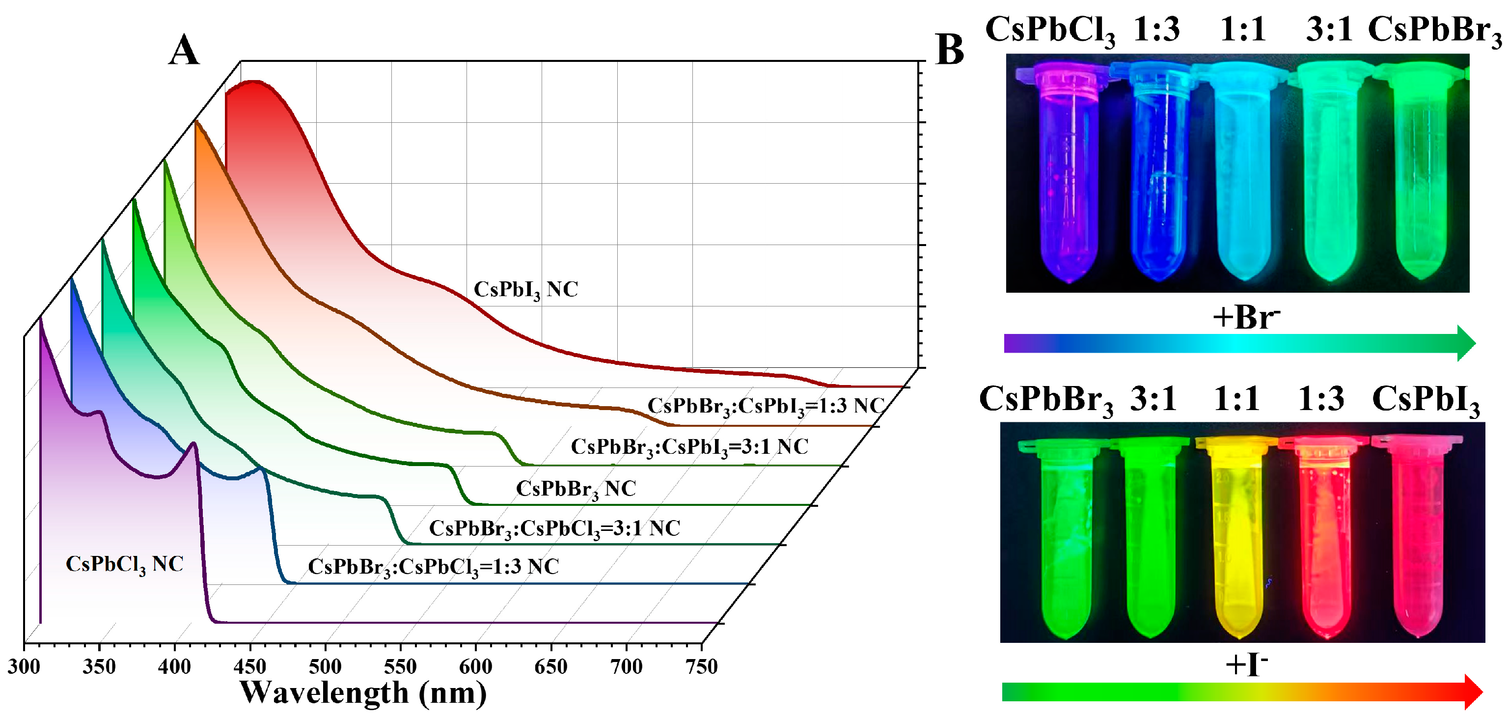
In light of the ionic nature of perovskite and the variability of its surface ligands, anion exchange reactions readily occur between perovskite materials with diverse halogens. The common method adopted by researchers is to add metal halide salts of different halogens such as CuX2 [57], KX [9], AlX3 [58], and ZnX2 [55] to perovskite NCs, then stir the mixture for a period of time before using centrifugal separation to obtain perovskite with different halogen components. Rather than following this approach, we instead mixed two types of perovskite nanocrystals with different halogens, achieving differences in luminescence via ion exchange. The UV-vis spectra of the solutions of perovskite NCs with different halogen contents exhibit different absorption peak positions (Figure 4A). These solutions are composed of CsPbCl3, CsPbBr3 and CsPbCl3 in volume ratios of 1:3 and 3:1, CsPbBr3, CsPbBr3 and CsPbI3 in volume ratios of 3:1 and 1:3, CsPbI3 NCs, corresponding to the positions of the respective leap peaks at 402 nm, 420 nm, 484 nm, 506 nm, 520 nm, 585 nm and 676 nm. Afterwards, based on the Einstein photoelectric effect and the Kubelka-Munk equation [59], the linear region of the absorption edge in the UV-Vis spectra was extrapolated to the energy axis intercept, which was used to estimate the surface optical band gaps of perovskite NCs with different halogen components as 3.03 eV, 2.84 eV, 2.49 eV, 2.37 eV, 2.33 eV, 2.02 eV, and 1.76 eV, respectively. Certain samples were observed to feature two sharp exciton absorption peaks, while others appeared to be relatively smooth, which we attributed to the varying extent of quantum confinement effects caused by differences in size, concentration, and homogeneity of the NCs. Perovskite nanocrystal solutions mixed in varying volume ratios behaved differently when stimulated with 365 nm UV lamps. As illustrated in Figure 4B, CsPbCl3 NCs are purple, and gradually change to blue and then green as Br- increases when mixed with CsPbBr3, while CsPbBr3 NCs are green and gradually change to yellow-orange and finally red CsPbI3 as I− increases when mixed with CsPbI3. The mixing of CsPbCl3 with CsPbI3 NCs results in fluorescence extinction rather than fluorescence emission. According to our investigation, a plausible explanation is that the Cl− and I− radii are sufficiently distinct from each other that the mixing process may cause them to enter each other’s crystal structures in such a way as to cause damage. Thus, there is no very effective means of making CsPbCl3 coexist with CsPbI3 while maintaining two different fluorescence emissions at the same time.
The states of the CsPbX3 (X = Cl, Br, I) NCs in different solvents were compared, as shown in Figure S4. During these experiments, it was found that the NCs were more soluble in hexane than in water, and were more readily dispersed in hexane. The NCs dispersed in both solvents emitted light in similar colors under UV lamp irradiation. After one day, the CsPbCl3 and CsPbBr3 dispersed in water continued to emitted relatively strong light, while the CsPbI3 NCs no longer emitted red light and behaved much less stably. The more stable CsPbBr3 NCs were selected to test the photoresponse current density and electrochemical impedance spectra (EIS), as shown in Figure S5. The EIS spectra of CsPbBr3 NCs exhibited a certain semicircular arc, indicating the presence of charge transfer resistance. In order to capture the photocurrent generated by the light signal and to exclude other influences, the photocurrent distribution is normally recorded at regular intervals when the light source is switched on. As depicted in Figure S5B, when the light source was switched off, the recorded photocurrent density was almost zero, while when the light source was switched on again after 30 s, the current increased instantaneously. When the light source was switched off every 30 s, the current decreased instantaneously. This further confirms that the CsPbBr3 perovskite material has suitable carrier migration efficiency with charge transport properties. Thus, CsPbBr3 NCs could be promising in the field of photoelectric catalysis. Perovskite NCs with different halogen fractions feature diverse fluorescence emission and contribute to the construction of light-emitting diodes. Moreover, analogous to conventional semiconductor NCs, halide perovskite NCs exhibit good homogeneity and monodispersity along with a well-defined cubic shape, which might be promote self-assembly for use as building blocks in ordered superstructures such as superlattices. The degree of ordering of the perovskite superstructure affects the optoelectronic properties, and as such can be used to alter the performance of functional electronic devices.
3. Materials and Methods
3.1. Chemicals
Cesium carbonate (Cs2CO3, Aladdin, 99.9%), lead acetate trihydrate (Pb(CH3COO)2·3H2O, Aladdin, 99.99%), sodium iodide (NaI, Macklin, 99.99%), oleic acid (OA, Aladdin, AR), oleylamine (OAm, Aladdin, 80~90%), 1-octadecene (ODE, Aladdin, >90%(GC)), benzoyl bromide (C6H5COBr, Aladdin, 97%), benzoyl chloride (C6H5COCl, Aladdin, 99%), n-hexane (Aladdin, >99%). All reagents labeled Aladdin are from Aladdin Reagent (Shanghai) Co., Ltd., Shanghai, China. The reagent marked Macklin is from Shanghai Macklin Biochemical Co., Ltd., Shanghai, China.
3.2. Synthesis Scheme of All-Inorganic Perovskite Nanocrystals
3.2.1. Preparation of Benzoyl Iodine
The benzoyl iodine was synthesized following the method reported by Muhammad Imran. In a typical synthesis, sodium iodide (3 g, 0.2 mmol) and benzoyl chloride (1.4 mL) were mixed in a 20 mL vial. The mixture was stirred vigorously at 75 °C on a hot plate for 5 h. With heating and stirring, the mixture changed from white to orange red color, manifesting the successful synthesis of benzoyl iodine. Then, the mixture was gradually cooled to room temperature and 5 mL of anhydrous ODE was added to the vial. The solution was filtered by a polytetrafluorethylene membrane with a 0.45 μm pore size to obtain clear benzoyl iodine, which was stored in vacuum for further use.
3.2.2. Synthesis of CsPbX3 (X = Cl, Br, I) Nanocrystals (NCs)
CsPbX3 (X = Cl, Br, I) nanocrystals (NCs) were synthesized via the previously published procedure [60] with modifications. In a 50 mL three-necked round-bottom flask, 0.016 g Cs2CO3, 0.076 g Pb(CH3COO)2·3H2O, 0.3 mL OA, 1 mL OAm, and a variable amount of ODE (5 mL for CsPbCl3 and CsPbBr3 NCs, 8 mL for CsPbI3 NCs) were loaded and dried under vacuum (−0.05~0.08 MPa) at 130 °C for 1 h. When the reaction mixture had solubilized completely, the flask was heated up to 165~200 °C under N2 flow; (the specific reaction temperatures are 200 °C for CsPbCl3 NCs, 170 °C for CsPbBr3 NCs and 165 °C for CsPbI3 NCs, respectively). Subsequently, benzoyl halides (1.8 mmol benzoyl chloride, 0.6 mmol benzoyl bromide, and 0.6 mmol benzoyl iodine) were swiftly injected. The reaction mixture was cooled immediately to room temperature using an ice bath for CsPbBr3 and CsPbI3 NCs, while the CsPbCl3 NCs were cooled after 20 s to obtain crude solutions.
3.2.3. Isolation of CsPbX3 (X = Cl, Br, I) Nanocrystals (NCs)
First, 5 mL of n-hexane was added to the CsPbCl3 and CsPbBr3 NC crude solutions, while 2 mL solvent was added to the CsPbI3 NC solution. Next, the solution was centrifuged at 6000 rpm for 5 min. The supernatant was discarded and the precipitate was centrifuged again at 6000 rpm for 3 min without additional solvent; residual supernatant was removed with a paper tissue. Later, the precipitate was redispersed by adding 500 μL of n-hexane and centrifuged again at 4000 rpm for 10min in order to separate larger particles. The resulting supernatants of CsPbBr3 and CsPbI3 NCs were collected, while the supernatant of the CsPbCl3 NCs was discarded. Next, 2 mL n-hexane was loaded into the precipitate to redisperse the CsPbCl3 NCs, followed by centrifuging at 4000 rpm for 10 min, and the supernatant was collected in a vial. Finally, CsPbX3 (X = Cl, Br, I) NCs were diluted with n-hexane (500 μL, 1 mL, and 800 μL for CsPbCl3, CsPbBr3, and CsPbI3 NCs, respectively).
3.2.4. Anion Exchange Reactions
In brief, CsPbBr3 was mixed with CsPbCl3 NCs taking different volume ratios. CsPbBr3 was blended with CsPbI3 NCs according to different volume ratios. When the anion exchange was complete, the solutions were transformed for 20~60 min into CsPbBrxCl3−x (0 < x < 3) and CsPbBryI3−y (0 < y < 3) NCs, respectively.
3.3. Materials Characterization
3.3.1. Transmission Electron Microscopy (TEM) Characterization
TEM images were acquired on a JEOL JEM-1400 Plus electron microscope (JEOL, Beijing, China) equipped with a thermionic gun at an accelerating voltage of 120 kV. The samples of nanocrystals were prepared by depositing a diluted nanocrystal suspension in n-hexane onto carbon-coated copper grids. The size distribution images of NCs were calculated using Nano Measurer software version 1.02.0005.
3.3.2. X-ray Diffraction (XRD) Characterization
XRD analysis was recorded on a Bruker D8 ADVANCE X-ray diffractometer (Bruker, Karlsruhe, Germany) with Cu-Kα radiation (λ = 1.54056 Å, 40 kV and 40 mA). NC specimens for the XRD measurements were prepared by drop-casting a concentrated NC suspension in n-hexane onto a substrate of SiO2/Si. XRD data analysis was conducted using Jade 6.5 software.
3.3.3. Fourier Transform Infrared (FTIR) Spectroscopy Characterization
Fourier transform infrared (FTIR) spectroscopy data were obtained utilizing a Nicolet 6700 Fourier transform infrared spectrometer (Thermo Fisher Scientific, Waltham, MA, USA) at room temperature. The wave number range of the instrument was set to 400 to 4000 cm−1, the scanning speed was set to 1 time/s, and the maximum resolution was 0.019 cm−1. According to the working principle of interferometer interference frequency modulation, the light emitted from the lamp is turned into interferometric light by a Michelson interferometer, then the interferometric light is allowed to irradiate the sample. The receiver receives the interferometric light, which contains information about the materials, which is then converted into a Fourier transform by the computer software to obtain a spectral diagram of the sample. For the test, a highly concentrated n-hexane dispersion solution of CsPbBr3 perovskite nanocrystals was applied to a glass slice, left to dry, and then tested.
3.3.4. X-ray Photoelectron Spectroscopy (XPS) Characterization
The XPS spectra of perovskite nanocrystals were obtained using an AXIS SUPRA X-ray photoelectron spectrometer (Kratos Analytical, a Shimadzu Group Company, Manchester, UK) equipped with a Thermo Scientific Kα spectrometer and a monochromatic Al-Kα X-ray source. The data were converted to VGD format and processed utilizing Avantage software version 5.9922. The binding energy scale was internally referenced to the C1s peak (binding energy for C−C = 284.8 eV).
3.3.5. Fluorescence Spectrum Measurements
The UV-vis absorption spectra were carried out using a Shimadzu UV-1800 spectrophotometer with UVProbe 2.52 software. The steady-state photoluminescence (PL) spectra were measured on a Shimadzu RF-6000 spectrophotometer with LabSolutions RF software, using an excitation wavelength (λex) of 350 nm for CsPbCl3 and 450 nm for CsPbBr3 and CsPbI3. Time-resolved photoluminescence spectra (TRPL) were collected via single photon counter. In the procedure of optical characterization, samples were prepared by diluting NCs solutions in n-hexane in quartz cuvettes with a path length of 10 mm.
3.3.6. (Photo) Electrochemistry Measurements
A Zennium electrochemical workstation (Kronach, Germany, Zahner Company) was used to obtain photocurrent and electrochemical impedance curves of halide perovskite NCs. The measurement was performed in a three-electrode setup with a working electrode of the sample, a platinum disk counter-electrode, and a reference electrode of Ag/AgCl (saturated KCl) (EAg/AgCl = +0.1989V vs. NHE) in the (photo) electrochemical electrolyte (0.5 M Na2SO4). For photocurrent measurement, the light source was a 405 nm LED, and the light intensity was tested with a Newport photometer. Electrochemical impedance spectra were measured in 0.5 M Na2SO4 at −0.1 V vs. NHE with an amplitude of 10 mV (frequency: 100 mHz~20 kHz).
4. Conclusions
In conclusion, monodisperse all-inorganic halide perovskite nanocrystals (NCs) with a homogeneous cubic morphology, concentrated size distribution, and cubic crystal structure were synthesized using a modified hot injection method and independently modulating the ratios of cesium, lead, and halogen precursors. Moreover, we were able to achieve relevant information on the surface functional groups via FTIR spectroscopy, which demonstrated the effective protonation of OAm acting as a surface ligand. Different halogen components contribute to variations in the band gap of the perovskite NCs, and consequently to varying emission and absorption peak positions in the respective fluorescence spectra and UV-vis absorption spectra. Furthermore, in the fluorescence lifetime curve the fluorescence lifetime is larger, with a red shift of the fluorescence wavelength (band gap) and more slow decay. Nanocrystals mixed from distinct volume ratios undergo anion exchange reactions, and consequently exhibit various absorption peaks. In addition, the solution is capable of adjusting color from violet to green and from green to red under the stimulation of a UV lamp, covering essentially the entire visible light range. Photocurrent and electrochemical impedance tests indicate that our work can be expected to advance the potential of halide perovskite materials for photoelectric catalysis applications.
Supplementary Materials
The following supporting information can be downloaded at: https://0-www-mdpi-com.brum.beds.ac.uk/article/10.3390/catal13071041/s1, Figure S1: (A,B) XRD patterns of halide perovskite nanocrystals with different halogen composition; Figure S2: XPS spectra of CsPbX3 (X = Cl, Br, I) nanocrystals. (A) Full spectra, (B) Cs 3d, (C) Pb 4f, (D) Cl 2p, (E) Br 3d, (F) I 3d; Figure S3: (A) UV-vis absorption spectra and (B) Absorbance versus photon energy and the determined bandgap Eg of halide perovskite nanocrystals with different halogen components. Figure S4: Images of CsPbX3 (X = Cl, Br, I) nanocrystals in different solvent (water and n-hexane) under sunlight and 365 nm UV lamp, respectively; Figure S5: (A) Transient photocurrent responses to on-off illumination of CsPbBr3 nanocrystals electrodes at −0.1 V versus NHE in neutral water (0.5 M Na2SO4). (B) Electrochemical impedance spectra (Nyquist plot) of CsPbBr3 nanocrystals.
Author Contributions
Y.L. (Yong Liu) conceived the project and material synthetic design. X.W. and J.H. performed the experiments, sample testing, data collection, and analysis. X.W. and Y.L. (Yuqing Li) discussed the data and performed formal analyses. X.W., W.L. and Y.L. (Yong Liu) wrote, reviewed, and edited the manuscript. All authors have read and agreed to the published version of the manuscript.
Funding
This work was financially supported by the National Natural Science Foundation of China (52072281, Y.L.), the Major Program of the National Natural Science Foundation of China (22293021, Y.L.), and the National Innovation and Entrepreneurship Training Program for College Students (No. S202210497011, Y.L.). Y.L. gratefully acknowledges the Youth Innovation Research Fund project of the State Key Laboratory of Advanced Technology for Materials Synthesis and Processing, Wuhan University of Technology.
Data Availability Statement
Data are available in a publicly accessible repository that does not issue DOIs or on request from the corresponding author.
Acknowledgments
We are grateful to the School of Chemistry and Chemical and Life Sciences of Wuhan University of Technology for providing UV-Vis and PL characterization and to the Center for Materials Research and Analysis of Wuhan University of Technology Materials for FTIR testing.
Conflicts of Interest
The authors declare no conflict of interest.
References
- Akkerman, Q.A.; Manna, L. What Defines a Halide Perovskite? ACS Energy Lett. 2020, 5, 604–610. [Google Scholar] [CrossRef] [PubMed]
- Zhang, J.; Zhong, Y. Origins of p-Doping and Nonradiative Recombination in CsSnI3. Angew. Chem. Int. Ed. Engl. 2022, 61, e202212002. [Google Scholar] [PubMed]
- Saparov, B.; Mitzi, D.B. Organic-Inorganic Perovskites: Structural Versatility for Functional Materials Design. Chem. Rev. 2016, 116, 4558–4596. [Google Scholar] [CrossRef] [PubMed]
- Ceratti, D.R.; Tenne, R.; Bartezzaghi, A.; Cremonesi, L.; Segev, L.; Kalchenko, V.; Oron, D.; Potenza, M.A.C.; Hodes, G.; Cahen, D. Self-Healing and Light-Soaking in MAPbI3: The Effect of H2O. Adv. Mater. 2022, 34, e2110239. [Google Scholar] [CrossRef] [PubMed]
- Li, Y.; Ding, T.; Luo, X.; Tian, Y.; Lu, X.; Wu, K. Synthesis and Spectroscopy of Monodispersed, Quantum-Confined FAPbBr3 Perovskite Nanocrystals. Chem. Mater. 2019, 32, 549–556. [Google Scholar] [CrossRef]
- Seth, S.; Ahmed, T.; De, A.; Samanta, A. Tackling the Defects, Stability, and Photoluminescence of CsPbX3 Perovskite Nanocrystals. ACS Energy Lett. 2019, 4, 1610–1618. [Google Scholar] [CrossRef]
- Fu, Y.; Jiang, X.; Li, X.; Traore, B.; Spanopoulos, I.; Katan, C.; Even, J.; Kanatzidis, M.G.; Harel, E. Cation Engineering in Two-Dimensional Ruddlesden-Popper Lead Iodide Perovskites with Mixed Large A-Site Cations in the Cages. J. Am. Chem. Soc. 2020, 142, 4008–4021. [Google Scholar] [CrossRef]
- Protesescu, L.; Yakunin, S.; Bodnarchuk, M.I.; Krieg, F.; Caputo, R.; Hendon, C.H.; Yang, R.X.; Walsh, A.; Kovalenko, M.V. Nanocrystals of Cesium Lead Halide Perovskites (CsPbX3, X = Cl, Br, and I): Novel Optoelectronic Materials Showing Bright Emission with Wide Color Gamut. Nano Lett. 2015, 15, 3692–3696. [Google Scholar] [CrossRef]
- Guhrenz, C.; Benad, A.; Ziegler, C.; Haubold, D.; Gaponik, N.; Eychmüller, A. Solid-State Anion Exchange Reactions for Color Tuning of CsPbX3 Perovskite Nanocrystals. Chem. Mater. 2016, 28, 9033–9040. [Google Scholar] [CrossRef]
- Akkerman, Q.A.; D’Innocenzo, V.; Accornero, S.; Scarpellini, A.; Petrozza, A.; Prato, M.; Manna, L. Tuning the Optical Properties of Cesium Lead Halide Perovskite Nanocrystals by Anion Exchange Reactions. J. Am. Chem. Soc. 2015, 137, 10276–10281. [Google Scholar] [CrossRef]
- Liu, F.; Zhang, Y.; Ding, C.; Kobayashi, S.; Izuishi, T.; Nakazawa, N.; Toyoda, T.; Ohta, T.; Hayase, S.; Minemoto, T.; et al. Highly Luminescent Phase-Stable CsPbI3 Perovskite Quantum Dots Achieving Near 100% Absolute Photoluminescence Quantum Yield. ACS Nano 2017, 11, 10373–10383. [Google Scholar] [CrossRef]
- Liu, H.; Liu, Z.; Xu, W.; Yang, L.; Liu, Y.; Yao, D.; Zhang, D.; Zhang, H.; Yang, B. Engineering the Photoluminescence of CsPbX3 (X = Cl, Br, and I) Perovskite Nanocrystals Across the Full Visible Spectra with the Interval of 1 nm. ACS Appl. Mater. Interfaces 2019, 11, 14256–14265. [Google Scholar] [CrossRef] [PubMed]
- Jiang, Y.; Sun, C.; Xu, J.; Li, S.; Cui, M.; Fu, X.; Liu, Y.; Liu, Y.; Wan, H.; Wei, K.; et al. Synthesis-on-Substrate of Quantum Dot Solids. Nature 2022, 612, 679–684. [Google Scholar] [CrossRef] [PubMed]
- Yettapu, G.R.; Talukdar, D.; Sarkar, S.; Swarnkar, A.; Nag, A.; Ghosh, P.; Mandal, P. Terahertz Conductivity within Colloidal CsPbBr3 Perovskite Nanocrystals: Remarkably High Carrier Mobilities and Large Diffusion Lengths. Nano Lett. 2016, 16, 4838–4848. [Google Scholar] [CrossRef] [PubMed]
- Zhang, X.; Xu, B.; Wang, W.; Liu, S.; Zheng, Y.; Chen, S.; Wang, K.; Sun, X.W. Plasmonic Perovskite Light-Emitting Diodes Based on the Ag-CsPbBr3 System. ACS Appl. Mater. Interfaces 2017, 9, 4926–4931. [Google Scholar] [CrossRef]
- Zhang, J.; Zhao, W.; Olthof, S.; Liu, S.F. Defects in CsPbX3 Perovskite: From Understanding to Effective Manipulation for High-Performance Solar Cells. Small Methods 2021, 5, e2100725. [Google Scholar] [CrossRef]
- Duan, C.; Cui, J.; Zhang, M.; Han, Y.; Yang, S.; Zhao, H.; Bian, H.; Yao, J.; Zhao, K.; Liu, Z.; et al. Precursor Engineering for Ambient-Compatible Antisolvent-Free Fabrication of High-Efficiency CsPbI2Br Perovskite Solar Cells. Adv. Energy Mater. 2020, 10, 2000691. [Google Scholar] [CrossRef]
- Zhang, J.; Hodes, G.; Jin, Z.; Liu, S.F. All-Inorganic CsPbX3 Perovskite Solar Cells: Progress and Prospects. Angew. Chem. Int. Ed. 2019, 58, 15596–15618. [Google Scholar] [CrossRef]
- Ramasamy, P.; Lim, D.H.; Kim, B.; Lee, S.H.; Lee, M.S.; Lee, J.S. All-Inorganic Cesium Lead Halide Perovskite Nanocrystals for Photodetector Applications. Chem. Commun. 2016, 52, 2067–2070. [Google Scholar] [CrossRef]
- He, Q.; Chen, G.; Wang, Y.; Liu, X.; Xu, D.; Xu, X.; Liu, Y.; Bao, J.; Wang, X. CsPbX3-ITO (X = Cl, Br, I) Nano-Heterojunctions: Voltage Tuned Positive to Negative Photoresponse. Small 2021, 17, e2101403. [Google Scholar] [CrossRef]
- Li, X.; Wang, Y.; Chen, T.; Xu, T.; Ye, S.; Liu, R.; Sun, Z.; Tan, C.; Lv, X.; Yang, J.; et al. Unencapsulated CsPbClBr2 Film Photodetectors Grown by Thermal Vacuum Deposition Exhibit Exceptional Environmental Stability in High-Humidity Air. ACS Appl. Energy Mater. 2022, 5, 8709–8716. [Google Scholar] [CrossRef]
- Wang, Z.; Yang, J.; Li, M.; Zeng, X.; Pi, M.; Liu, Z.; Liu, J.; Zhang, D.; Hu, Z.; Du, J. Low Threshold and Ultrastability of One-Step Air-Processed All-Inorganic CsPbX3 Thin Films toward Full-Color Visible Amplified Spontaneous Emission. ACS Appl. Mater. Interfaces 2022, 14, 26904–26912. [Google Scholar] [CrossRef] [PubMed]
- Nie, L.; Yu, X.; Ge, Y.; He, D.; Zhu, X.; Liu, H.; Guo, H.; Zhao, F.; Yu, S.; Qiu, J.; et al. Highly Stable and Controllable Lasing Actions from PVDF Encapsulated CsPbBr3 Perovskite Microcrystals. J. Mater. Chem. C 2022, 10, 16301–16308. [Google Scholar] [CrossRef]
- Wang, Y.; Li, X.; Nalla, V.; Zeng, H.; Sun, H. Solution-Processed Low Threshold Vertical Cavity Surface Emitting Lasers from All-Inorganic Perovskite Nanocrystals. Adv. Funct. Mater. 2017, 27, 1605088. [Google Scholar] [CrossRef]
- Yang, X.; Zhang, X.; Deng, J.; Chu, Z.; Jiang, Q.; Meng, J.; Wang, P.; Zhang, L.; Yin, Z.; You, J. Efficient Green Light-Emitting Diodes Based on Quasi-Two-Dimensional Composition and Phase Engineered Perovskite with Surface Passivation. Nat. Commun. 2018, 9, 570. [Google Scholar] [CrossRef]
- Cao, Y.; Wang, N.; Tian, H.; Guo, J.; Wei, Y.; Chen, H.; Miao, Y.; Zou, W.; Pan, K.; He, Y.; et al. Perovskite Light-Emitting Diodes Based on Spontaneously Formed Submicrometre-Scale Structures. Nature 2018, 562, 249–253. [Google Scholar] [CrossRef]
- Lin, K.; Xing, J.; Quan, L.N.; de Arquer, F.P.G.; Gong, X.; Lu, J.; Xie, L.; Zhao, W.; Zhang, D.; Yan, C.; et al. Perovskite Light-emitting Diodes with External Quantum Efficiency Exceeding 20 Percent. Nature 2018, 562, 245–248. [Google Scholar] [CrossRef]
- Wang, K.; Zhang, H.; Gu, Z. All-Inorganic Perovskite Nanocrystal Materials: New Generation of Scintillators for High Quality X-ray Imaging. Sci. Bull. 2019, 64, 1205–1206. [Google Scholar] [CrossRef]
- Ma, W.; Jiang, T.; Yang, Z.; Zhang, H.; Su, Y.; Chen, Z.; Chen, X.; Ma, Y.; Zhu, W.; Yu, X.; et al. Highly Resolved and Robust Dynamic X-ray Imaging Using Perovskite Glass-Ceramic Scintillator with Reduced Light Scattering. Adv. Sci. 2021, 8, e2003728. [Google Scholar] [CrossRef]
- Yang, H.; Li, H.; Yuan, R.; Chen, J.; Zhao, J.; Wang, S.; Liu, Y.; Li, Q.; Zhang, Z. A Novel Scintillation Screen for Achieving High-Energy Ray Detection with Fast and Full-Color Emission. J. Mater. Chem. C 2021, 9, 7905–7909. [Google Scholar] [CrossRef]
- Chan, K.K.; Giovanni, D.; He, H.; Sum, T.C.; Yong, K.-T. Water-Stable All-Inorganic Perovskite Nanocrystals with Nonlinear Optical Properties for Targeted Multiphoton Bioimaging. ACS Appl. Nano Mater. 2021, 4, 9022–9033. [Google Scholar] [CrossRef]
- Kar, M.R.; Kumar, S.; Acharya, T.K.; Goswami, C.; Bhaumik, S. Highly Water-Stable, Luminescent, and Monodisperse Polymer-Coated CsPbBr3 Nanocrystals for Imaging in Living Cells with Better Sensitivity. RSC Adv. 2023, 13, 5946–5956. [Google Scholar] [CrossRef] [PubMed]
- Mohapatra, A.; Kumar, S.; Acharya, T.K.; Goswami, C.; Bhaumik, S. Highly Stable Multi-Encapsulated Red-Emitting Cesium Lead Halide Nanocrystals for Efficient Copper Ion Detection and Imaging in Live Cells. J. Alloys Compd. 2023, 947, 169453. [Google Scholar] [CrossRef]
- Xiao, M.; Hao, M.; Lyu, M.; Moore, E.G.; Zhang, C.; Luo, B.; Hou, J.; Lipton-Duffin, J.; Wang, L. Surface Ligands Stabilized Lead Halide Perovskite Quantum Dot Photocatalyst for Visible Light-Driven Hydrogen Generation. Adv. Funct. Mater. 2019, 29, 1905683. [Google Scholar] [CrossRef]
- Yang, Y.; Li, Y.; Gong, W.; Guo, H.; Niu, X. Cobalt-doped CsPbBr3 perovskite quantum dots for photoelectrocatalytic hydrogen production via efficient charge transport. Colloids Surf. A 2023, 663, 131083. [Google Scholar] [CrossRef]
- Pavliuk, M.V.; Abdellah, M.; Sá, J. Hydrogen Evolution with CsPbBr3 Perovskite Nanocrystals under Visible Light in Solution. Mater. Today Commun. 2018, 16, 90–96. [Google Scholar] [CrossRef]
- Xu, Y.F.; Yang, M.Z.; Chen, B.X.; Wang, X.D.; Chen, H.Y.; Kuang, D.B.; Su, C.Y. A CsPbBr3 Perovskite Quantum Dot/Graphene Oxide Composite for Photocatalytic CO2 Reduction. J. Am. Chem. Soc. 2017, 139, 5660–5663. [Google Scholar] [CrossRef]
- Hou, J.; Cao, S.; Wu, Y.; Gao, Z.; Liang, F.; Sun, Y.; Lin, Z.; Sun, L. Inorganic Colloidal Perovskite Quantum Dots for Robust Solar CO2 Reduction. Chemistry 2017, 23, 9481–9485. [Google Scholar] [CrossRef]
- Li, L.; Zhang, Z.; Ding, C.; Xu, J. Boosting charge separation and photocatalytic CO2 reduction of CsPbBr3 perovskite quantum dots by hybridizing with P3HT. Chem. Eng. J. 2021, 419, 129543. [Google Scholar] [CrossRef]
- Liu, H.; Bansal, S. Metal halide perovskite nanostructures and quantum dots for photocatalytic CO2 reduction: Prospects and challenges. Mater. Today Energy 2023, 32, 101230. [Google Scholar] [CrossRef]
- Das, S.; Paul, T.; Maiti, S.; Chattopadhyay, K.K. Ambient Processed CsPbX3 Perovskite Cubes for Photocatalysis. Mater. Lett. 2020, 267, 127501. [Google Scholar] [CrossRef]
- Gao, G.; Xi, Q.; Zhou, H.; Zhao, Y.; Wu, C.; Wang, L.; Guo, P.; Xu, J. Novel inorganic perovskite quantum dots for photocatalysis. Nanoscale 2017, 9, 12032–12038. [Google Scholar] [CrossRef]
- Xin, B.; Pak, Y.; Mitra, S.; Almalawi, D.; Alwadai, N.; Zhang, Y.; Roqan, I.S. Self-Patterned CsPbBr3 Nanocrystals for High-Performance Optoelectronics. ACS Appl. Mater. Interfaces 2019, 11, 5223–5231. [Google Scholar] [CrossRef] [PubMed]
- Fu, X.; Zhang, C.; Peng, Z.; Xia, Y.; Zhang, J.; Luo, W.; Zhan, R.; Li, H.; Wang, Y.; Zhang, D. Self-Assembly and Photoactivation of Blue Luminescent CsPbBr3 Mesocrystals Synthesized at Ambient Temperature. J. Mater. Chem. C 2018, 6, 1701–1708. [Google Scholar] [CrossRef]
- Liu, X.; Li, J.; Cui, X.; Wang, X.; Yang, D. Strategies for the Preparation of High-Performance Inorganic Mixed-Halide Perovskite Solar Cells. RSC Adv. 2022, 12, 32925–32948. [Google Scholar] [CrossRef] [PubMed]
- Wang, Y.; Yasar, M.; Luo, Z.; Zhou, S.; Yu, Y.; Li, H.; Yang, R.; Wang, X.; Pan, A.; Gan, L.; et al. Temperature Difference Triggering Controlled Growth of All-Inorganic Perovskite Nanowire Arrays in Air. Small 2018, 14, e1803010. [Google Scholar] [CrossRef] [PubMed]
- Dong, S.; Hu, Z.Y.; Wei, P.; Han, J.; Wang, Z.; Liu, J.; Su, B.L.; Zhao, D.; Liu, Y. All-Inorganic Perovskite Single-Crystal Photoelectric Anisotropy. Adv. Mater. 2022, 34, e2204342. [Google Scholar] [CrossRef] [PubMed]
- Sun, S.; Yuan, D.; Xu, Y.; Wang, A.; Deng, Z. Ligand-Mediated Synthesis of Shape-Controlled Cesium Lead Halide Perovskite Nanocrystals via Reprecipitation Process at Room Temperature. ACS Nano 2016, 10, 3648–3657. [Google Scholar] [CrossRef]
- Pan, A.; He, B.; Fan, X.; Liu, Z.; Urban, J.J.; Alivisatos, A.P.; He, L.; Liu, Y. Insight into the Ligand-Mediated Synthesis of Colloidal CsPbBr3 Perovskite Nanocrystals: The Role of Organic Acid, Base, and Cesium Precursors. ACS Nano 2016, 10, 7943–7954. [Google Scholar] [CrossRef]
- Chen, D.; Fang, G.; Chen, X.; Lei, L.; Zhong, J.; Mao, Q.; Zhou, S.; Li, J. Mn-Doped CsPbCl3 Perovskite Nanocrystals: Solvothermal Synthesis, Dual-Color Luminescence and Improved Stability. J. Mater. Chem. C 2018, 6, 8990–8998. [Google Scholar] [CrossRef]
- Chen, M.; Zou, Y.; Wu, L.; Pan, Q.; Yang, D.; Hu, H.; Tan, Y.; Zhong, Q.; Xu, Y.; Liu, H.; et al. Solvothermal Synthesis of High-Quality All-Inorganic Cesium Lead Halide Perovskite Nanocrystals: From Nanocube to Ultrathin Nanowire. Adv. Funct. Mater. 2017, 27, 1701121. [Google Scholar] [CrossRef]
- Han, D.; Imran, M.; Zhang, M.; Chang, S.; Wu, X.G.; Zhang, X.; Tang, J.; Wang, M.; Ali, S.; Li, X.; et al. Efficient Light-Emitting Diodes Based on in Situ Fabricated FAPbBr3 Nanocrystals: The Enhancing Role of the Ligand-Assisted Reprecipitation Process. ACS Nano 2018, 12, 8808–8816. [Google Scholar] [CrossRef]
- Chen, X.; Wang, Z. Investigating Chemical and Structural Instabilities of Lead Halide Perovskite Induced by Electron Beam Irradiation. Micron 2019, 116, 73–79. [Google Scholar] [CrossRef] [PubMed]
- Dang, Z.; Shamsi, J.; Akkerman, Q.A.; Imran, M.; Bertoni, G.; Brescia, R.; Manna, L. Low-Temperature Electron Beam-Induced Transformations of Cesium Lead Halide Perovskite Nanocrystals. ACS Omega 2017, 2, 5660–5665. [Google Scholar] [CrossRef] [PubMed]
- Li, F.; Liu, Y.; Wang, H.; Zhan, Q.; Liu, Q.; Xia, Z. Postsynthetic Surface Trap Removal of CsPbX3 (X = Cl, Br, or I) Quantum Dots via a ZnX2/Hexane Solution toward an Enhanced Luminescence Quantum Yield. Chem. Mater. 2018, 30, 8546–8554. [Google Scholar] [CrossRef]
- Yu, Y.; Zhang, D.; Kisielowski, C.; Dou, L.; Kornienko, N.; Bekenstein, Y.; Wong, A.B.; Alivisatos, A.P.; Yang, P. Atomic Resolution Imaging of Halide Perovskites. Nano Lett. 2016, 16, 7530–7535. [Google Scholar] [CrossRef]
- Chen, Y.-C.; Chou, H.-L.; Lin, J.-C.; Lee, Y.-C.; Pao, C.-W.; Chen, J.-L.; Chang, C.-C.; Chi, R.-Y.; Kuo, T.-R.; Lu, C.-W.; et al. Enhanced Luminescence and Stability of Cesium Lead Halide Perovskite CsPbX3 Nanocrystals by Cu2+-Assisted Anion Exchange Reactions. J. Phy. Chem. C 2019, 123, 2353–2360. [Google Scholar] [CrossRef]
- Uddin, M.A.; Glover, J.D.; Park, S.M.; Pham, J.T.; Graham, K.R. Growth of Highly Stable and Luminescent CsPbX3 (X = Cl, Br, and I) Nanoplates via Ligand Mediated Anion Exchange of CsPbCl3 Nanocubes with AlX3. Chem. Mater. 2020, 32, 5217–5225. [Google Scholar] [CrossRef]
- Zhang, Y.; Wang, X.; Chen, Y.; Gao, Y. Improved Electroluminescence Performance of Quantum Dot Light-Emitting Diodes: A Promising Hole Injection Layer of Fe-doped NiO Nanocrystals. Opt. Mater. 2020, 107, 110158. [Google Scholar] [CrossRef]
- Imran, M.; Caligiuri, V.; Wang, M.; Goldoni, L.; Prato, M.; Krahne, R.; De Trizio, L.; Manna, L. Benzoyl Halides as Alternative Precursors for the Colloidal Synthesis of Lead-Based Halide Perovskite Nanocrystals. J. Am. Chem. Soc. 2018, 140, 2656–2664. [Google Scholar] [CrossRef]
Scheme 1.
Schematic diagram of the synthesis procedure of all-inorganic CsPbX3 (X = Cl, Br, I) perovskite NCs.
Scheme 1.
Schematic diagram of the synthesis procedure of all-inorganic CsPbX3 (X = Cl, Br, I) perovskite NCs.

Figure 1.
(A–C) TEM images of CsPbCl3, CsPbBr3, and CsPbI3 NCs (scale bar: 100 nm) and (D–F) their size distribution diagrams.
Figure 1.
(A–C) TEM images of CsPbCl3, CsPbBr3, and CsPbI3 NCs (scale bar: 100 nm) and (D–F) their size distribution diagrams.

Figure 2.
(A–C) XRD patterns of CsPbX3 (X = Cl, Br, I) NCs and (D) FTIR spectra of CsPbBr3 NCs.

Figure 3.
(A–C) UV-vis absorption and photoluminescence (PL) spectra of CsPbCl3, CsPbBr3, and CsPbI3 NCs and (D) time-resolved photoluminescence (TRPL) spectra of CsPbCl3, CsPbBr3, and CsPbI3 NCs. The small circles with a dot in the center represent raw data and the solid lines are the corresponding fitted curves.

Figure 4.
(A) UV-vis absorption spectra of perovskite NCs solutions with different volume ratios of CsPbBr3 with CsPbCl3, CsPbBr3, and CsPbI3; (B) image of mixed solutions of CsPbBr3 and CsPbCl3 NCs with different volume ratios and mixture of CsPbBr3 and CsPbI3 NCs with different volume ratios under 365 nm ultraviolet lamp excitation.

Disclaimer/Publisher’s Note: The statements, opinions and data contained in all publications are solely those of the individual author(s) and contributor(s) and not of MDPI and/or the editor(s). MDPI and/or the editor(s) disclaim responsibility for any injury to people or property resulting from any ideas, methods, instructions or products referred to in the content. |
© 2023 by the authors. Licensee MDPI, Basel, Switzerland. This article is an open access article distributed under the terms and conditions of the Creative Commons Attribution (CC BY) license (https://creativecommons.org/licenses/by/4.0/).
Share and Cite
MDPI and ACS Style
Wang, X.; Liu, W.; He, J.; Li, Y.; Liu, Y. Synthesis of All-Inorganic Halide Perovskite Nanocrystals for Potential Photoelectric Catalysis Applications. Catalysts 2023, 13, 1041. https://0-doi-org.brum.beds.ac.uk/10.3390/catal13071041
AMA Style
Wang X, Liu W, He J, Li Y, Liu Y. Synthesis of All-Inorganic Halide Perovskite Nanocrystals for Potential Photoelectric Catalysis Applications. Catalysts. 2023; 13(7):1041. https://0-doi-org.brum.beds.ac.uk/10.3390/catal13071041
Chicago/Turabian StyleWang, Xiaoqian, Wanli Liu, Jiazhen He, Yuqing Li, and Yong Liu. 2023. "Synthesis of All-Inorganic Halide Perovskite Nanocrystals for Potential Photoelectric Catalysis Applications" Catalysts 13, no. 7: 1041. https://0-doi-org.brum.beds.ac.uk/10.3390/catal13071041
Note that from the first issue of 2016, this journal uses article numbers instead of page numbers. See further details here.