Article

Pure, Size Tunable ZnO Nanocrystals Assembled into Large Area PMMA Layer as Efficient Catalyst

1
LCP-A2MC, Institut Jean Barriol, Université de Lorraine, 1 Bd Arago, 57070 Metz, France
2
L2n, Lumière, Nanomatériaux, Nanotechnologies, ICD, CNRS, Université de Technologie de Troyes, 10004 Troyes, France
3
Institut Jean Lamour, Université de Lorraine, UMR CNRS 7198, BP 70239, 54506 Vandœuvre-lès-Nancy, France
*
Author to whom correspondence should be addressed.
The dagger symbol (†) placed after the name of a dead person.
Submission received: 24 January 2019 / Revised: 1 February 2019 / Accepted: 1 February 2019 / Published: 7 February 2019
(This article belongs to the Special Issue Photocatalysis Science and Engineering in Europe)

Abstract

:
Here, we demonstrate for the first time a strategy to self-assemble ZnO nanoparticles (NP) on a large area by a facile one-step process. First, rough and random ZnO nanocrystals (NC), were produced by free-stabilizing aqueous synthesis. Therefore, a post thermal treatment at various temperatures ranging from 80 to 800 °C was necessary to obtain size-tunable and photoluminescent crystalline NP. The fabricated NP had both efficient UV photoluminescence and photocatalytic activity by photo-degradation of Methylene Blue (MB) dye. The annealed NP showed an absorption blue shift in the UV region with decreasing size. This shift was attributed to high quantum confinement effect since ZnO NP diameter reached values lower than the Bohr radius of ZnO (~2.7 nm). The photocatalytic activity displayed dependency on the particle’s size, number, and crystallinity. Subsequently, the NP were self-assembled inside poly(methyl methacrylate) (PMMA) nanoholes. Subsequently, large area substrate of homogenous properties ZnO NP was obtained. Moreover, the synthesis facility, photoemission and photocatalytic properties of ZnO NP could be a new insight into the realization of high performance and low cost UV laser devices.

1. Introduction

In recent years, the fabrication of highly luminescent semiconductor nanostructures with an efficient photocatalytic activity has emerged at the level of science and technology. These semiconducting nano-scaled systems have received growing interest, due to their optical and electronic properties [1,2,3,4]. Moreover, as nanocrystal entities they have enhanced quantum efficiency with a tunable band gap [5], which enable them to participate in wide fields of applications, favoring catalytic, as well as optoelectronic operations [6,7,8,9]. Among various semiconductor photocatalysts, zinc oxide nanocrystals are special wurtzite n-type semiconductors that attracted attention, due to their various impressive electrical and physical characteristics. Precisely, ZnO nanostructures have a direct and wide band gap (~3.37 eV) besides their high exciton binding energy (60 meV) and rich defect chemistry structures [10]. They also possess a strong oxidizing power and superior UV emission characteristics, in addition to high stability and room temperature luminescence [11,12]. These features, allowed by the large quantum confinement, make them greatly promising and attractive materials for various devices, such as ultraviolet photodetectors, photovoltaic devices, sensors, solar cells, laser diodes and photocatalysts [13,14]. Besides, ZnO nano-objects can be used in several biological activities as they are biocompatible materials of low toxicity [15].
Nanocrystals (NC) sometimes referred to quantum dots (QD) in the literature, are extremely ultrathin and highly crystalline semiconductors with restricted 3D motion (i.e., electrons in the conduction band and holes in the valence band in the 3D of excitons) [16]. When NC size is comparable to the Bohr radius (Bohr radius of ZnO bulk ranges between 2.34 nm [17], to 3 nm [18]) in a way that it is too small to match the wavelength of the electrons, its optical properties, as well as the excitation and emission bands are widely affected. This implies quantum confinement features [19], which lead to a transition from continuous to discrete energy levels in the absorption spectrum [20]. The band gap of the semiconductor could be shifted, due to the size constraint, creating excitons with a significant electron-hole binding energy in the excited electronic state [3]. Many synthesis pathways allowed to fabricate ZnO nanostructures such as: vapor phase oxidation [21], thermal vapor transport and condensation (TVTC) [22,23], micro-emulsion [24], polyol methods [25], sol-gel method [26,27], sonochemical or microwave-assisted synthesis [28,29,30,31], hydrothermal synthesis [32,33], spray pyrolysis [34], chemical vapor deposition [35,36], thermal decomposition of organic precursor [37], direct precipitation [38], double solvothermal method [39], and many other techniques. However, the majority of these approaches are multi-step and low-throughput processes. Moreover, most of them involved complex equipment, toxic reactants, such as lithium hydroxide (LiOH) which acts as explosive [31,40], and deteriorating organic solvents, such as methanol, ethanol, or chloroform- instead of water. On the other hand, the synthesis of ZnO nanostructures in alcoholic mediums has received extensive acceptance because of the faster nucleation and growth of NP in such solvents as compared to water. The latter is also avoided because it facilitates the transfer of the excited charge carriers of the corresponding NP to the surrounding molecules, leading to its luminescence quenching [40]. Due to the high surface tension of ZnO NP, several preparation methods are a surfactant-assisted synthesis that requires capping or stabilizing agents, such as poly vinyl pyridine (PVP), polyethylene glycol (PEG), etc., in order to obtain small, spherical, and non-aggregated nanoparticles [41,42]. Using these additives induces a large amount of organic impurities complexing the chemistry of the reaction, and restricting the accessibility to the nanocrystal surface (bad sensing operations).
Despite the excessive efforts to fabricate ultra-small, efficient catalyst and luminescent quantum dots in aqueous solutions, no research has so far achieved this performant product of ZnO nanocrystalline NP, via simple synthesis route and under soft conditions, including temperature, pressure, time, equipment used, and materials.
Moussodia et al. have modified the ZnO NP surface by the silanization method in order to obtain a water soluble and stable product useful for biological labels [43]. They covalently linked the ZnO surface by a PEG-siloxane where the aim of the surface modification was to maintain the surface luminescence properties of the synthesized ZnO QD that may be striked and destroyed by the water molecules. However, the initial synthesis was carried out in an alcoholic medium, and the final obtained product was not absolutely pure as they introduced organic molecules throughout the fabrication process, in the time homogeneous and pure nanomaterials are needed as a result for various applications. The organic additives may modify the physico-chemical properties of the synthesized nanostructures, limiting their applications especially as catalysts and lasers [44].
In another report concerning the fabrication of water soluble ZnO QD, Fu et al. have synthesized water-stable ZnO QD. The addition of oleic acid and/or diethanoamine (DEA) was indeed to adopt high stability and water dispersion availability preserving the intensity fluorescence property [45].
In most current fabrication methods, a high temperature procedure, either at high temperature fabrication process or high temperature post-synthesis treatment of the ZnO is needed for attaining good quality material [46]. On the other hand, applied science is currently recommending plastics and flexible electronics [47,48,49], which emphasizes on the necessity of adapting alternate treatment processes that ensure the synthesis of well crystalline ZnO nanostructures keeping the temperature at the low value [50].
In our research work, small, uniform and highly stable ZnO NP were fabricated by hydrothermal method using water as a non-contaminating solvent that acts as a self-capping, stabilizing and directing agent, where the nanocrystals’ shape and size could be controlled. Without the usage of stabilizing, this method is a promising alternative guide for preparation of pure ZnO NP at a relatively low temperature using soft conditions. It is simple, green, and high throughput method, in addition to the good stability and purity of products.
Although, ZnO luminescence has been the subject of studies for several decades where the mechanisms responsible for many of its emission properties in relation to its photocatalytic activity are still a matter of discussion. To our knowledge, no reports in the literature have succeeded to aqueously fabricate highly luminescent ZnO NP with high photocatalytic activities, since the photocatalysis (PC) and the photoluminescence (PL) are two processes that depend respectively on the separation and recombination of the photo-induced charge carriers which are competitive mechanisms. In this paper, we also efficiently describe how polymer self-assembly procedures can be adapted for ZnO NP synthesis, serving as a model system for other oxide nanostructures hydrothermally synthesized in water, and the optical characterizations could be successfully attained.

2. Results

2.1. Optimisation of Synthesis

In order to set up the parameters of the synthesis reaction, the photoemission of the prepared ZnO NP solutions after UV excitation was examined.
Generally, ZnO photoluminescence is marked by two regions, the first is a confined peak corresponding to the near band edge (NBE) emission in the ultraviolet region of the emission spectrum, which characterizes the exciton radiative recombination of the electrons and holes, and the second is a large intense defect level (DL) band in the visible zone [51,52,53].
This photoemission study aimed to examine the effects of the time and temperature of the reaction on the structural and optical properties of ZnO nanostructures.

2.1.1. Synthesis Time

For examining the hydrothermal reaction time on the nanostructures of ZnO, the reaction temperature was fixed at 80 °C, and the reaction time was prolonged from 20 min to 1 h where the UV exciton luminescence of the zinc oxide nanocrystals (ZnO NC) was examined.
The PL measurements of the as-synthesized NC prepared at 80 °C during 20 and 60 min showed no obvious UV emission relative to the exciton luminescence in both conditions. The only observed peak in the UV region was the Raman signature of the water solvent at ~365 nm (3372 cm−1), while no emission band for ZnO NP was observed (Figure 1a).
Therefore, extending the reaction time does not enhance the crystal growth of ZnO nanostructures to evidence their exciton emission. Energy transfer may be considered as the cause of quenching the ZnO exciton emission, by which the water molecules could highly react with the NP in the solution, transforming all the excitation energy between the surface water units to obtain the Raman scattering, preventing the ZnO electron excitation process, as well as its luminescence. Consequently, the absence of PL band could be attributed to the overlapping of the Raman of -OH bond with the exciton of the ZnO NC preventing its luminescence. In addition, ZnO NP are highly charged particles considered as donors because they normally have luminescence in the UV-Vis region, while water is considered as an acceptor because it absorbs in the UV-Vis-NIR region. As reported by Meyer et al. and Dulub et al., electron-hole (e-h+) pairs are generated in ZnO nanostructures upon UV illumination in the photoluminescence measurements, where the water molecules are physisorbed on the surface of particles. The nearby water molecules on each neighboring ZnO nano-object create a hydrogen bond between them, stimulating the dissociation of water units, which in turn capture these e-h+ pairs at the same moment, leading to the decrease in the carrier density in ZnO. As a result, gradual decay of the current through the charge transfer occurs, preventing the emission of the nanostructures [54,55,56]. In this context, the major concern in ZnO NC is the diminishing luminescence of the nanoparticles, due to the effect of the water solvent. Ahn et al. referred this effect to the exchange of the water-ZnO ionic species at the oxygen defect levels in ZnO NP leading to a slow photo-response [57]. In another report, Mahamuni et al. and Jin et al. referred the quenching of UV luminescence to the poor crystalline quality of the as-synthesized nanoparticles [58,59].
In conclusion, the reaction time in our experiments has no considerable effect on building up ZnO NC to differentiate its photoluminescence in such conditions.

2.1.2. Synthesis Temperature

Since 80 °C is lower than the boiling temperature of water (100 °C), higher synthesis temperatures were adjusted in order to decrease the effect of water molecules on the ZnO luminescence. Two curing temperatures above 100 °C (110 °C and 150 °C) were investigated to test its effect on the luminescence of the as-prepared nanostructures.
As shown in Figure 1b, increasing the synthesis temperatures allowed us to identify the ZnO exciton peak. Obviously, it could be identified that by increasing the reaction temperature from 80 to 150 °C passing through 110 °C, the Raman peak intensity of water decreased while ZnO peak prevailed, thus the exciton emission became more and more clear. As a result, it could be concluded that the temperature is a key factor in our reaction, where the effect of adsorbing solvent was less effective with increasing temperatures. We also suggest that, temperature increase allows the formation of ZnO nanostructures of better crystallinity.
Concerning the effect of the reaction time and that of the temperature on the desired reaction, we found that prolonging the reaction time at 80 °C had no significant influence on the characteristics of the obtained ZnO nanostructures, however raising the reaction temperature had.
Although, it is well known that with increasing hydrothermal temperature and/or time of the reaction results in unfavorable grain growth of the particles, and increases the average crystalline size of the reaction products [60]. Yet, the smaller the nanoparticles are, the more interesting they are in catalysis applications, where the photocatalytic degradation behaviors become more efficient at smaller sizes by which the active surface atoms increase, triggering the surface to gain much tension, and therefore offering higher catalytic efficiency [61,62,63]. For this reason, the obtained ZnO NC at lower temperatures might be more interesting, dealing with smaller nanostructures. As an indication of the smaller NC sizes obtained at 80 °C temperature reaction is the quenching UV luminescence, referring to Biju et al. whom they reported that smaller NC will have a higher surface over volume ratio favoring the quenching effect [64,65].
Thereby, to avoid the exciton emission quenching of small sized ZnO nanostructures synthesized at 80 °C, the bond between the hydroxide of the solvent with the NP should be broken. For this aim, the solution was heated for one hour at a temperature of 150 °C using a regular heating plate. As a result of the annealing process, the excess solvent was evaporated, thus the quenching effect was also eliminated. Consequently, the crystallinity of the NP could be enhanced.
PL measurements were applied to the annealed solutions and are shown in Figure 1c. The emergence of the exciton peak at ~380 nm after post thermal treatment of the samples was clearly observed. Therefore, the quenching luminescence of the small sized NP synthesized at 80 °C was avoided after post-thermal treatment.
Accordingly, to detect the exciton emission of small ZnO NP synthesized in water, the synthesis should be adapted by two conditions: Even at a temperature smaller than the normal boiling temperature of the solvent with a post-thermal treatment (T = 80 °C + annealing), or at a temperature higher than the solvent’s boiling temperature without any further operations.
It is worth to note that the exciton emission of the annealed ZnO synthesized at 80 °C showed the most intense UV peak among others (Figure 1d). This is referred to the fact that the annealing process promotes the removal of additional complex impurities existing in the solution by transforming the residual Zn(OH)2 and ZnNO3 complexes into ZnO nanoparticles, increasing the latter’s density number in the solution. The small red shift in the exciton emission may be due to the slight aggregation caused by annealing.
In this simple strategy, the characteristics of ZnO NC could be controlled throughout the synthesis process according to the aimed appliances.

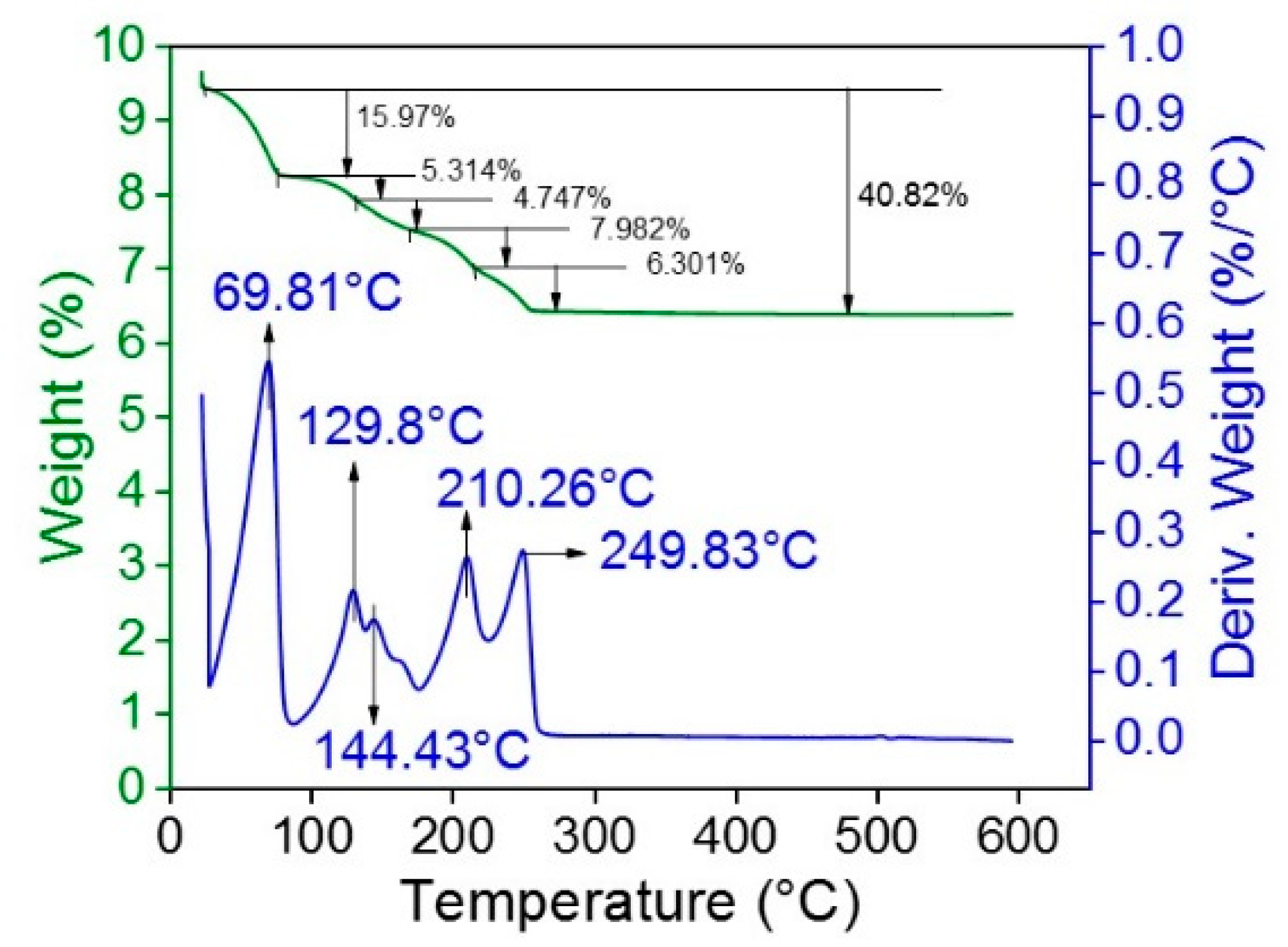
2.2. Structural Properties

To better understand the PL features, the raw powders were extracted by filtration. After washing with isopropanol, the collected powders were annealed at different temperatures to gain more purity, to increase the number of the synthesized ZnO nanostructures, and to enhance their crystallinity. The overall achieved powders were able to be embedded in several solvents, such as water, isopropanol, ethanol, and others..., depending on the desired application. Tuning the physical and chemical properties of the fabricated ZnO nanostructures through the chemical reaction synthesis has gained attention and reported by adapting different ways, such as controlling the ZnO growth using dopants, or by thermal annealing of the pure ZnO nanostructures [66,67]. This latter is favorable since the physical and optical properties of the initially synthesized nanostructures could be mainly conserved. Thus the effect of the annealing process on the as-synthesized ZnO samples was examined.
Thermogravimetric analysis of non-annealed powders synthesized at 80 °C for 20 min, was tested in order to examine their thermal behavior by probing the thermal decomposition and stability of our product with temperature.
The TGA profile, shown in Figure 2, shows a continuous loss of weight with five alterations occurring at approximately 70, 130, 144, 210, and 250 °C.
Above this value, no loss of mass was observed. Heating up to 250 °C results into a loss of mass of 41% of the total mass of the raw synthesized sample. Therefore, the annealing temperature of 250 °C could be considered as an optimum value for annealing since it provides stable ZnO nanostructures.
On this basis, XRD measurements were performed for ZnO powders synthesized at 80 °C and annealed at various temperatures in order to investigate their structures and crystallinity. Table 1 showed that the raw synthesis product is mainly composed of Zn5(NO3)2(OH)8·2H2O crystalline structure, which is embedded with only 9% of amorphous ZnO nanoparticles.
The formation of nanoparticles and the amorphous feature can be attributed to both broadness and weakness of peak intensities in the 2θ range 10–18 Degree (Figure 3a and Figure A1 of the Appendix B).
Subsequently, thermal annealing allowed the destruction of Zn5(NO3)2(OH)8·2H2O phase and a complete disappearance above 250 °C giving rise to 100% ZnO nanoparticles. Thus, the ZnO percentage in the obtained powders increased from 9% without post-thermal annealing into 10, 30, 75, and 99% for the following annealing at 80, 100, 150, and 250 °C, respectively. Moreover, with increasing the annealing temperature, the amorphous ZnO NP became crystalline, in relation to the appearance of narrow, intense and periodic peaks, which were attributed to ZnO crystalline nanostructures.
In addition, the ZnO phase displayed the same structure for all the samples. Precisely, the five observed diffraction peaks after annealing, including (100), (002), (101), (102) and (110), match well the wurtzite hexagonal structure of the ZnO NP, having predominantly (101) preferred orientation as a result of minimizing the internal stress and surface energy through this plane [68]. After raising the annealing temperatures beyond 150 °C, no peaks corresponding to impurities were observed in the patterns, confirming the high phase purity of the samples, due to the deduction of chemical residues and impurities.
Using Bragg’s law, the lattice constants were assessed from the hkl indices in the XRD spectrum. The obtained values of “a” and “c” of the different ZnO samples do not correspond to ZnO bulk structure [68], as shown in Table 1.
Figure 3b illustrates the evolution of the (101) preferred lattice plane of the ZnO nano-objects (before and after annealing at different temperatures). As the annealing temperature rises, a slight increase in the 2θ position of the (101) plane was observed with an increased peak intensity, in relation to better crystallinity and higher amount of crystalline ZnO nanoparticles oriented at this plane direction as assessed before.
The crystallite size of the mostly crystalline nanoparticles annealed at 150, 250, 500 and 800 °C depicted in Figure 3c were estimated using the Scherrer Equation (1):
D = K λ β cos θ   ,
where D is the crystallite size, K is a numerical factor referred to the crystallite-shape constant (0.94), λ is the wavelength of the X-rays,   β is the full-width at half-maximum (FWHM) for the most intense peak (101) in radians and θ is the Bragg angle. The crystallite sizes were 35, 50, and 57 nm for the samples annealed at 150, 250, and 500 °C respectively, to reach a size higher than 100 nm, after annealing at 800 °C.
The cell volume (v) and the number of atoms per unit cell (n) for the ZnO samples with the hexagonal form depicted in Figure 3d were estimated using Equations (2) and (3) respectively [69,70]:
V = 3 3 2 a 2 c   ,
n = 4 π 3 V ( D 2 ) 3   ,
As the crystallite size increased, the cell volumes decreased followed by the increase in the number of atoms per unit cell. These theoretical results are in agreement with the percentage composition measurements (derived from the XRD) of crystalline ZnO with respect to the complex structures initially obtained after synthesis.

2.3. Optical Properties

SEM images in Figure 4, for samples shown Figure 3, also confirm the increase of ZnO nanoparticles size with increasing the annealing temperature. Indeed, without annealing we only observe the Zn5(NO3)2(OH)8·2H2O microstructure.
ZnO nanostructures are very small at this condition (without annealing) and they are embedded inside. When the temperature increases, Zn5(NO3)2(OH)8·2H2O is decomposed, melted and calcined. We can observe ZnO as small nano-objects on the surface of melted microstructure in Figure 4b. From the Figure 4b until Figure 4g, only ZnO nanoparticles appeared with a continuous size increase respectively. Precisely, the nanoparticles became gradually more numerous, crystalline and bigger when annealed up to 250 °C. After the excessive increase in the annealing temperatures to 500 °C and 800 °C, the size further increased, whereas the density of particles started to decrease. This may be linked to the effect of fusion and coalescence of the nanoparticles at high temperatures. Interestingly, at 800 °C, nanostructures could melt and lead then to the fusion of nanoparticles, ending up in bigger nanoparticles (larger than 100 nm). At the same time, 500 and 800 °C could be high enough to recrystallize the nanoparticles after melting, retaining the high crystallinity behaviour observed by XRD.
For a better investigation of ZnO photoluminescence characteristics, in addition to SEM, samples were also observed by TEM. Subsequently, their absorption spectra were then collected by UV-Vis spectrophotometry measurements. To make it possible, the synthesized powders were dispersed in water to adapt a suitable environment for characterization with an ultrasonic aid to achieve un-aggregated and homogeneous nanostructures.
In Figure 5a, the non-annealed sample showed the Zn5(NO3)2(OH)8·2H2O microstructures as observed and discussed before in the SEM images of Figure 4a.
In this figure, ZnO quantum dots of very small size (<1 nm) appear as black dots doping the microstructure. After post-thermal treatment at 80 °C, the TEM image of the corresponding sample, shown in Figure 5b, revealed an increase in the crystallinity that was also significant in the crystal diffraction image in Figure 5c. The as-synthesized and annealed sample at 80 °C showed very small sized particles (<1 nm). Here, we can talk about ZnO nanoclusters. Above 80 °C as annealing condition, the nanostructures started growing until reaching the nanoscale. Thus, the produced nanoparticles gradually coalesced and aggregated as temperature increased until reaching a large size of ~200 nm at 800 °C. These observations are in consistent with XRD and SEM measurements.
UV-Vis absorption (Abs.) measurements were performed on the as-synthesized samples of Figure 4. Figure 6a shows an absorption band centered at 365 nm for the non-annealed sample, which is a characteristic peak of ZnO NP (blue shifted with respect to the value of bulk ZnO “385 nm” might be due to a high quantum confinement effects) [71].
After annealing at 80, 100, 150, 250, and 500 °C, the absorption peaks of the samples shifted from 365 nm to 375, 378, 371, 375, and 378 nm, respectively. It is well known in the literature that ZnO is UV absorbing, which results into the appearance of an exciton peak centered at 380 nm in the photoluminescence spectrum. This exciton peak based on the physics of semiconductor materials is usually red-shifted than the absorption peak. Indeed, ZnO absorbs at 365 nm. When UV excited, it fluoresces light at lower energy than it absorbs. This is called radiative deexcitation. One can note the Abs. band broadness at 800 °C, due to the non-homogenous size presence. From there, we conclude that the thermal annealing is a critical parameter that mainly affects both the structural and optical properties of ZnO nanoparticles [72].
Based on the Abs. band, we calculated the optical band gap energy according to the relation of photon energy in quantum mechanics (see Equation (4))
E g = h c λ   ,
where Eg is the optical band gap energy (in eV), h is Plank’s constant (6.626 × 10⁻³⁴ Joules.sec), c is the velocity of light (2.99 × 10⁸ m·s−1) and λ is the wavelength absorption peak value (in nm). The optical band gap energies are listed in Table 2.
A gradual decrease of Eg from 3.4 to 3.28 eV is observed with increasing annealing temperatures. The highest value of 3.4 eV determined at 80 °C, is higher than the theoretical Eg value of ZnO (3.34 eV). This result could indicate the quantum confinement that appears when the nanoparticle’s size matches or it is lower than the Bohr radius of the material as assessed before. The band gap energy of the ZnO NP annealed at 800 °C could not be determined, due to the largely wide absorption band, which does not allow a precise determination of the band gap energy.

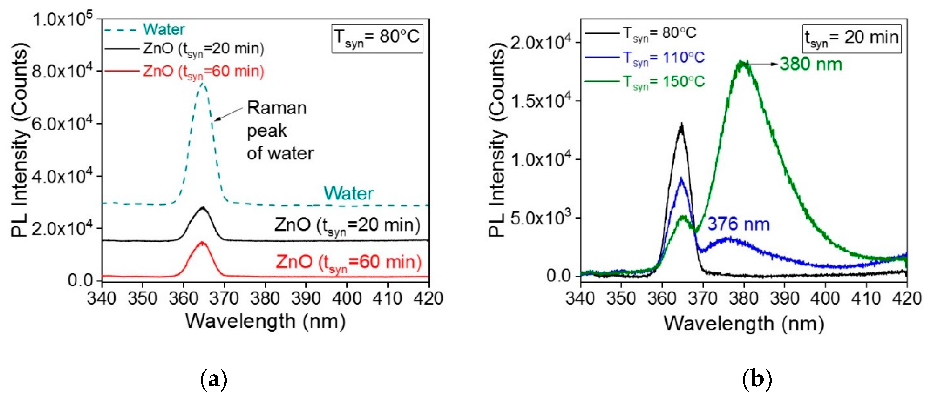
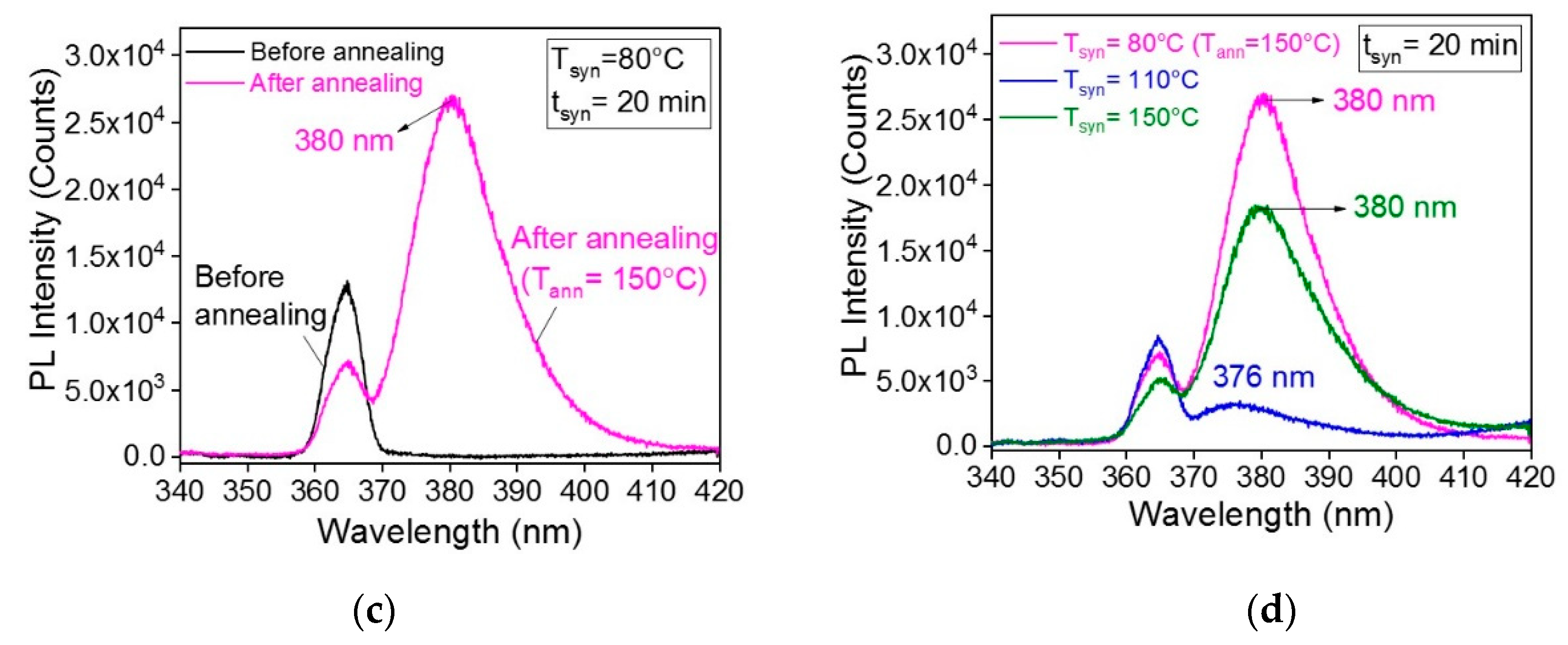
2.3.1. Photoluminescence Measurements

After Abs. measurements, the photoemission of the same samples (with the same annealing parameters) was tested under 365 nm UV-lamp and the images are shown in Figure 7.
In a research work concerning the importance of water soluble ZnO QD combined into biological systems, Lu et al. have recommended the different color emission of the QD rather than the blue emission [73]. Since the UV irradiation of the biological cells reveals a blue light [73,74], it is worth to introduce different color emitters in such systems in order to distinguish between the obtained emissions. This results in enhanced investigations in biological labeling applications. The different colors obtained by our fabricated products reveal various optical properties, in relation to different dimensions of the nanoparticles. This could highly serve the above mentioned application, as well as many other operations.
One can observe UV and visible emission of ZnO nanoparticles in the images. Basically, the UV energy belongs to the band gap emission where the electrons in the conduction band and the holes in the valence band can recombine radiatively, to produce the luminescence of the exciton referring to the recombination in the near band edge (NBE) and suggesting the formation of well- crystallized ZnO QD [75].
On the other hand, the visible emission mainly originates from the intrinsic defect energy levels corresponding to oxygen vacancies VO, zinc vacancies VZn, oxygen interstitials Oi, zinc interstitials Zni, in addition to oxygen and zinc antisites (OZn and ZnO) [5,39,76,77,78,79]. More precisely, Zinc interstitials Zni and oxygen vacancies VO are the most proposed dominant luminescing defects, where the latest results from the recombination of electrons trapped in the singly ionized VO with the photoexcited holes [80]. Another possibility for the visible emission is the surface bonded hydroxides (OH–S) as reported by Norberg et al. [81]. Although different predictions of the mechanisms of the defect emissions, the proposals of the origin of visible luminescence are a subject of highly argumentative dispute, which is not yet clear. Similarly, for our fabricated samples, ZnO nanostructures exhibited an intense UV peak accompanied by a broad visible peak, as shown in Figure 8a.
The PL measurements showed no considerable UV peak for the non-annealed sample, due to its amorphous structure in addition to the Raman peak of the water solvent as discussed above. However, the UV luminescence was clearly identified after annealing of the powders, revealing the exciton emission of ZnO nanoparticles (Figure 8c). Upon annealing, the PL band position shifted from ~378 nm to ~382 nm, indicating a gradual increase in the size. One can also see in Figure 8b an increase of the intensity of UV emission band when temperature increased from 80 °C until 250 °C. Above this value, the intensity gradually decreased.
The emergence in the UV-PL intensity with the annealing temperature up to 250 °C is attributed to the annealing process, which acts as impurity removal and then increases the ZnO amount in the dispersed powder, increasing the radiative recombinations of their excitons.
However, it was previously shown in the TGA measurements in Figure 2 that no mass loss was observed above 250 °C, thus higher annealing temperatures will have no deal with the purification of the particles or transforming complexes into nanostructures. Therefore, the excessive increase in the annealing temperatures may affect the crystal itself, deforming its structure until coalescence, as shown in the TEM and SEM images. As a result, the radiative recombination decreases, which reflects weaker UV emission band.
The broad visible PL band related to the defects in all samples is ranged from green to orange emission regions with different intensities depending on the annealing temperature. The small shoulders included in the defect level band contribute to the noise interference and the technical imperfections.
The green emission normally corresponds to the intrinsic defect energy levels (oxygen vacancies VO resulting from the recombination of a photo-generated hole with the singly ionized charge state of this defect, and/or zinc vacancies VZn). Green defect emission peaks were also observed in comparable synthesis [39]. The orange emission is related to the excess of oxygen as interstitial defects [82,83,84,85], in addition to zinc interstitials and surface dislocations [86,87]. In some reports, yellow emissions were also observed and attributed to the oxygen interstitial defects, as well as to the presence of Zn(OH)2 and other impurities at the surface of the NP [88].
In our case, the defect level peak position was approximately the same for samples annealed in the range 80–500 °C, which indicates the constant local environment of the defect centers in our samples [89,90]. Annealing at 800 °C showed a slightly different contribution of the defects which is related to the variation in the crystal environment, due to the fusion of nanoparticles at this temperature.
The present small peaks at 730 nm and the other at ~755 nm correspond to the second order of the water solvent peak and the UV emission of the ZnO nanoparticles, respectively. The latest peak was also reported by Tonon et al. [91].
As a conclusion, the thermal annealing is necessary to obtain crystalline and efficiently photoluminescent ZnO nanostructures. Nevertheless, the temperatures must be ranged between 250 and 500 °C.

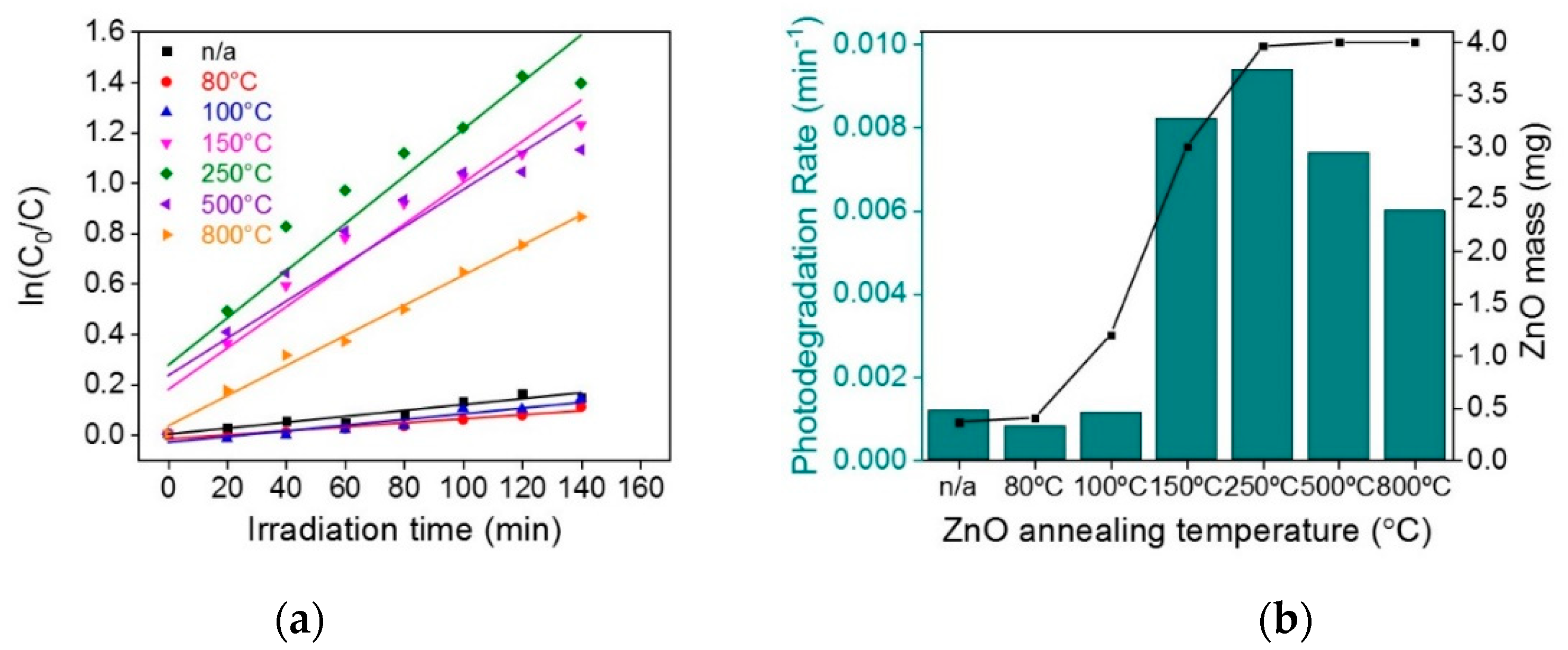
2.3.2. Photocatalytic Properties

Due to the small size of ZnO nanoparticles (<1 nm at 80 °C), that we were able to fabricate in the present work, which is required in photocatalysis analysis, we investigate here the performance of our samples as photo-catalysts. For this aim, we used methylene blue (MB) dye as a model for the catalysis study. The required mass of the catalyst was mixed with MB aqueous solution, and then irradiated with a wavelength of 365 nm at various time intervals. In the absence of the ZnO photocatalyst, the irradiated MB solution was found to be stable even after 120 min and the color of the MB solution remained the same. The corresponding absorption spectra of MB alone under UV irradiation are shown in the SI.
Knowing that each annealing temperature corresponds to a critical size and number of ZnO nanoparticles, the degradation efficiency was estimated by measuring the absorbance of MB in the presence of ZnO (before and after annealing). After the addition of ZnO nanoparticles, the solutions exhibited various photocatalytic activities. The height of the MB absorbance band centered at 664 nm decreased, which indicates the contribution of ZnO to the degradation of MB. At the end of the reaction, the solutions turned colorless indicating the total consumption of MB in the dispersions.
The MB degradation in the presence of the various ZnO samples studied before, are represented in the SI. We show the photocatalytic activity of the ZnO sample annealed at 250 °C over MB dye degradation in Figure 9.
The photocatalytic efficiency of these samples is illustrated via the percentage of degradation of MB dye and calculated using the following Equation:
Degradation   ( % ) = ( Abs t 0 Abs t f Abs t 0 ) × 100   ,
where Abst0 is the absorbance value of MB at t = 0 min of the photo-reaction, and Abstf is the value of absorbance at the final time of the reaction t = 140 min. The results are tabulated in Table 3.
The amount of the ZnO catalyst was 4 mg in all the samples, the percentage of ZnO weight in the powders used was estimated from the percentages obtained through the XRD measurement, and the results are listed in Table 3. The decrease in the MB absorbance became more efficient when the annealing temperature increases up to 250 °C. Beyond this temperature, the degradation of MB started to decrease.
Referring to the photocatalysis concept of ZnO, electrons and holes are generated on the conduction and valence bands, respectively, after illumination with sufficient UV light (Equation (6a)), where the efficiency of the photo-induced charge carriers counts on the intensity of incident photons with energy higher than or equals to the ZnO bandgap energy [92]. At the surface of the ZnO, oxygen acceptors could be reduced at the conduction band resulting in the formation of superoxide radical anion (O2−•), which may produce hydroxyl radicals (HO) (see Equations (6b) and (6c)). While the holes in the valence band react with the adsorbed water to form reactive hydroxyl radicals (HO) (Equation (6d)). The resulted radicals can directly oxidize the organic pollutants and have a powerful ability to degrade an organic dye of MB (Equation (6e)) [93,94]. The mentioned reactions are summarized below:
ZnO + hν → e + h+,
e + O2 → O2−•,
O2−• + H2O → HO,
h+ + H2O → HO,
O2−•/ HO + MB → oxidation products,
As a result, the nanostructures with smaller sizes have more energetic surface electrons and should have better photocatalytic activity. At the same time, the sample containing more of well dispersed and non-aggregated nanoparticles can absorb more light, which increases the photocatalytic activity. On this basis, ZnO nanoparticles annealed at 250°C showed the highest photocatalytic activity, in relation with the high number of well dispersed nanoparticles in this case. On the other hand, at higher annealing temperatures, the size increase leads to the decrease in the photocatalytic activity.
The photocatalytic degradation kinetics of MB in the presence of ZnO follows Langmuir-Hinshelwood kinetic model [95]:
r = d C d t = [ kKc 1 + Kc ] ,
where r is the photodegradation rate (slope of the first order equation calculated from lnC0/C = Kt), C is the reactant concentration at irradiation time t, k is the reactant rate constant and K is the adsorption coefficient of the reactant. Kc is nearly 1 at very small c leading to pseudo-first order kinetics equation, and therefore the rate expression is given by the equation:
ln C 0 C = K app t ,
where C0 is the equilibrium concentration of MB (t = 0 min) and C is the concentration at time t, and Kapp is the apparent pseudo-first order rate constant. The plot of the kinetic analysis of the ZnO NP annealed at different temperatures is shown Figure 10a stating a linear relationship between the MB concentration and the irradiation time.
The photodegradation rate is computed as a function of increasing annealing temperature of ZnO in Figure 10b. It is observed that the degradation rate is similar for the non-annealed and both the annealed ZnO ones at 80 and 100 °C. Further increase in the annealing temperatures significantly increased the photodegradation rate to reach its maximum at 250 °C. After this temperature, the photodegradation rate decreased. The kinetic rate constant and the linear regression coefficient (R2) of all ZnO NP are also listed in Table 3.
To better understand these observations, we tried to discuss the relation between ZnO photocatalytic efficiency and its amount in the powder dispersed in water for analysis. To make it possible, we described the ZnO mass change as a function of annealing temperature in relation to the photodegradation rate in the following manner:
  • Without and with annealing at 80 °C, ~9% (0.36 mg ZnO/4 mg) of ZnO nanostructures are present in the powder sample.
  • Annealing at 80 to 250 °C, ZnO percentage increased from 10% (0.4 mg ZnO/4 mg) to ~99% (3.96 mg ZnO/4 mg).
  • From 250 to 800 °C, ZnO percentage reached 100% (4 mg ZnO/4 mg) and remains constant.
Therefore, the PC activity of all samples could be discussed according to these three zones.
In the first range (1), knowing that the non-annealed samples are smaller in size, they allowed higher % of MB degradation than those annealed at 80 °C, due to higher surface area.
In the second zone (2), when the annealing temperature was raised, both the size and the number of nanoparticles increased, creating a competitive role between the dimension effect and the volume fraction effect; bigger nanoparticles should have less photocatalytic activity. In contrast, a dispersion containing a higher concentration of nanoparticles should have higher one. In our experiments, we observed an increase in the PC activity until reaching nearly an ideal photodegradation (100%) at an annealing temperature 250 °C. Here, the density effect dominated the size effect leading to better photocatalytic activity.
In the last region (3), the amount of ZnO nanoparticles is the same (4 mg), while their size increased with annealing effect. Due to the size effect at a constant number of particles, the photocatalytic activity gradually decreased.
In most photocatalysis studies, TiO2 is widely used for this aim. However, ZnO is an effective alternative, due to its comparative band gap energy and lower cost of fabrication [96,97]. In addition, ZnO is considered higher photoactive than TiO2 as reported by several scientists [98,99,100,101]. The higher photoactivity is referred to the higher efficiency to provoke the formation of photoexcited charge carriers [96,102]. The photocatalytic activity highly depends on the exposed surfaces of the catalyst which enhance its degradation efficiency [103,104], since the contaminant molecules to be degraded should adsorb on the catalyst surface for the above mentioned reactions to occur. Therefore, the catalyst surface area plays a decisive role for the photocatalyst’s efficiency, which is determined through the method of preparation of the catalyst. Previously, few reports were investigated using ZnO nanostructures aiming for the degradation of methylene blue under irradiation of UV light [105,106,107,108]. Talebian et al. reported the efficient photocatalytic activity of ZnO thin films by the degradation of MB dye after UV light illumination for 240 min [105]. Delgado et al. reported the synthesis of ZnO thin film by sol–gel process. The photocatalytic activity of ZnO over the degradation of MB was achieved within 5 h of UV light irradiation [108].
As the nanoparticles adapt higher surface to volume ratio compared to nanowires and thin films that are widely used in photocatalysis, ZnO NP could be the appropriate applicant for the adsorption of contaminants to achieve higher degradation rates with fewer irradiation times compared to other morphologies. This was evidence in our samples were the MB was completely degraded using the proper ZnO catalyst annealed at 250 °C adapting the best surface, size, number and crystallinity of particles. ZnO here exhibited a high photodegradation rate within ~100 min UV light irradiation to completely degrade the MB due in the solution.

2.3.3. Large Area Layer of ZnO NP

Fluorescent materials are considered as the dynamos for analysis in various of current lab-on-chip (LOC) devices [109]. These systems enable new structural and functional biomolecule studies, enhance chip-based bioanalytical assays, in addition to many other applications [110].
In this context, ZnO NP were assembled by PMMA as described in the materials and methods section aiming afterwards to use this system as a fluorescent material in bio-labeling or catalysis operations. Therefore, the obtained monolayer of ZnO NP-loaded poly(methyl methacrylate) (PMMA) was evaluated by photoluminescence measurements as illustrated in Figure 11.
As observed in the PL spectrum, the obtained ZnO NP have a UV emission at 393 nm, which corresponds to the exciton emission. The peak above 400 nm are due to noise interference and the technical imperfections.
The obtained ZnO-loaded PMMA system was consequently observed by optical microscopy and atomic force microscopy (AFM); the corresponding images are depicted in Figure 12. One can see the presence of ZnO NP as bright dots localized in the PMMA nanoholes in Figure 12a,b. Figure 12c also evidence the ZnO NP inside the PMMA holes. One can see in Figure 12d that ZnO NP are present into PMMA layer of ~90 nm thickness. The hydrophobic feature of PMMA against the hydrophilic one for ZnO could be of great interest for both local growth and characterization of materials only on ZnO. In addition to the production of pure and size-tunable ZnO with a step synthesis process, this result reflects the major novelty in the present paper because there is no such approach in the literature allowing the assembly of pure, stable and highly luminescent ZnO NP on a large area.

3. Materials and Methods

3.1. Fabrication of ZnO NC

The chemical reagents used in this synthesis were zinc nitrate hexahydrate, 98% extra pure (Zn(NO3)2·6H2O) and sodium hydroxide (NaOH) precursors purchased from ACROS Organics (Morris, NJ, USA) and Fisher Scientific (Bishop Meadow Rd, Loughborough LE11 5RG, Royaume-Uni) respectively without further purification. In the simple hydrothermal reaction, different curing temperatures were adapted throughout the synthesis (80 °C, 110 °C and 150 °C). Equal volumes of aqueous stock solutions Zn(NO3)2·6H2O (1 M) and NaOH (1 M) were mixed under constant stirring of 350 rpm and simple heating for 20 and 60 min where we obtained two different phase solutions: An upper liquid phase (supernatant) and a white precipitate (powder) that were further separated from each other by filtration step. This synthesis process is illustrated in Figure A2 in Appendix B. The remaining filtered powders were washed several times with deionized water (DI water) and isopropanol to evacuate the water adsorbed on the particles, and to remove the undesirable complex ions (Zn5(NO3)2(OH)8·2H2O in our case) that are considered as impurities possibly remaining in the prepared product. The quantum dots finally obtained in a powder form were directly calcined for 1 h in an oven under air at different annealing temperatures (80 °C, 100 °C, 150 °C, 250 °C, 500 °C, and 800 °C). The obtained powders were re-dispersed in water under sonication for 1 h without any further heating, to obtain homogeneous and ultrafine particles in the dispersion solution.

3.2. Self-Assembly of ZnO Nanostructures into Nanoporous PMMA Layer

The strategy of fabrication of ZnO mono layer was adapted from our previous studies [111,112,113,114]. A polymer/zinc nitrate dispersion was formed by mixing solutions of Zn(NO3)2·6H2O and poly (methyl methacrylate) (PMMA). The zinc nitrate solution was prepared by the dissolution of 20 mg of zinc precursor in 1ml of ethanol. Then, 1.5 mL of PMMA solution was added to the zinc nitrate and stirred for half an hour. Upon spin coating of the obtained PMMA/zinc nitrate dispersion on a silicon (Si) substrate (speed = 10,000 rpm, time = 30 sec and acceleration = 3000 rpm/sec), Zn2+-loaded PMMA micelles are formed on the whole substrate. Then, a drop of 0.1 M NaOH solution was deposited on the obtained substrate, and the Si-wafer was heated at 80 °C for 20 min to obtain the ZnO nanostructures.

3.3. Characterization

X-Ray diffraction (XRD,) measurements were performed using a powder diffractometer (X’pert PRO PANalytique,(Nancy, France) in reflection mode to study the structure of ZnO samples. The measurements were made under a voltage of 45KV and an intensity of 50 mA, in an angular range of 0 to 60° (0° < 2θ < 60°) using a copper source of λ = 1.54056 Å.
Thermal decomposition of the as-prepared ZnO samples was performed using a TA Instruments TGA 2050 Thermogravimetric Analyzer (Metz, France), coupling the heating rate with the mass loss. The thermal evolution of the natural materials was followed from room temperature up to 600 °C.
Transmission electron microscopy (TEM,) investigations were carried out using a JEM - ARM 200F Cold FEG TEM/STEM (Nancy, France) operating at 200 kV and equipped with a spherical aberration (Cs) probe and image correctors (point resolution 0.12 nm in TEM mode and 0.078 nm in STEM mode.
SEM images were acquired using HITACHI SU8030 SEMFEG (Troyes, France), with a typical accelerating voltage of 15KV having a large specimen stage with 110 mm traverse range in both of XY direction and a maximum 150 mm diameter sample exchange chamber as standard. The images were elaborated after depositing a drop of the solution on a silicon substrate and drying at room temperatures.
Dark-field images were obtained by using a straight BX51 Olympus optical microscope using a Halogen source.
AFM measurements were performed by a Nano-R2t AFM, operated in contact mode, and then color-balanced using the imageJ software.
UV-Vis absorption measurements were achieved to see the absorption of the NP using a UV-Visible spectrophotometer Specor 205 from Analytic-Jena (Metz, France), where the transmitted light was dispersed and analyzed by a CCD camera with a resolution of 1 nm. These measurements allow us to characterize the optical properties of ZnO NP giving information about the homogeneity and the size of the NC from their band gap width and the position of the peaks corresponding to the absorption of ZnO.
Photoluminescence measurements (PL) were carried out to estimate the optical characteristics of the ZnO exciton recombination using a He-Cd laser of wavelength 325 nm and photon energy 3.82 eV. The spectra were acquired in the range of 340–950 nm. The transmitted light was dispersed by the grating and analyzed by a CCD camera (Mrtz, France). The measurements were performed at room temperature (RT), and the PL data were collected under the same conditions, i.e., light path, excitation power, acquisition parameters, exposure time, and split front entrance, to exclude any other effect on the PL measurements.
The photocatalytic activity was investigated using 1 mL of methylene blue (MB) dye solution (5 × 10⁻⁴ M) and 1 mL of a ~0.267 × 10⁻³ g/L ZnO catalyst solution in a 1.0 cm quartz cuvette under UV irradiation using high intensity mercury-xenon lamp with a mercury line filter of 365 nm light segment. The absorbance of the blank reference sample (MB blue irradiated in the absence of the catalyst) was determined using a specific volume of the dye. The quartz cuvettes were 0.4 cm apart from the light source in order to avoid the diverging of light through the filter. During irradiation, the solution of ZnO/MB was magnetically stirred and the absorbance of MB was measured by UV–visible spectrometry after the addition of the catalyst for studying the reaction kinetics. The amount of ZnO NC and that of MB dye were kept constant through all the experiments.

4. Conclusions

In this paper, we presented an original approach for synthesizing large-area substrate of ZnO NP as catalyst and Lab-on-Chip system, which might be used to grow a wide range of nanomaterials, including metallic, magnetic, semiconductors, hybrids, etc. To make it possible, pure ZnO nanoparticles having different sizes ranged from ~1 nm to ~200 nm were first fabricated in water by a fast, economic and green synthesis way without the usage of ligands. High quantum confinement was observed for the smallest ZnO NP, in relation to a blue-shift of ~20 nm of the exciton peak. Precisely, an exciton absorption peak at ~365 nm was obtained for ZnO of ~1 nm diameter. To achieve this goal, two synthesis temperatures can be derived; the first temperature is lower than the boiling temperature (80 °C) of the solvent and allows the fabrication of small size of ZnO NP. The second temperature is higher than the solvent’s boiling T (150 °C) and corresponds to the post-thermal treatment temperature required to crystallize the NP after synthesis. Herein, the post-thermal treatment controls the as-synthesized particles, where the fabricated nanoparticles can be greatly used in wide fields of biological, photocatalytic, optical, and electronic applications. The ZnO NP were then self-assembled into PMMA layer using VIPS strategy in order to fabricate a large area substrate of ZnO. It is a challenge for us to use this approach in the future as a reference strategy for fabricating various semiconducting nanoparticles with such high controllability and efficacy.

Author Contributions

Writing—original draft preparation and formal analysis, I.S.; supervision, review and editing, S.A.; manipulation, I.S., N.B., E.-E.B., P.M. (Patrice Miska); validation, J.J.G., H.R., A.E.N., P.M. (Pierre Magri), S.J.

Funding

This research was funded by the doctoral school of Lorraine University (SEAMES).

Acknowledgments

The authors gratefully acknowledge Jaafar GHANBAJA (Lorraine University, IJL, CC3M) for his efforts in TEM measurements, Stéphane DALMASSO and Pascal FRANCHETTI (Lorraine University, IJB, LCP-A2MC) for their attempts in PL measurements. And Hassan KHODER (Lorraine University, IJB, CRM2) for his help in the XRD measurements.

Conflicts of Interest

The authors declare no conflict of interest. The funders had no role in the design of the study; in the collection, analyses, or interpretation of data; in the writing of the manuscript, or in the decision to publish the results.

Appendix A

Using Bragg’s law in Equation (A1), nλ = 2d sinθ
with the first order approximation n = 1, then d= λ/2sinθ. θ is assessed for each plane from the XRD patterns. The lattice constants a, b and c were assessed from the hkl Miller indices in the XRD spectrum using the formula associated with the hexagonal systems:
1/d2 = 4/3 ((h2 + hk + k2)/a2)) + l2/c2
Hence, the lattice constant “a” for the (100) plane is calculated by a = 2d/√3
For the (002) plane, the lattice constant “c” was calculated by c = 2d

Appendix B

Figure A1. XRD spectrum of the powdered ZnO NP synthesized at 80 °C and non-annealed. The red circles show broad and peak intensities, in relation to amorphous ZnO NP.
Catalysts 09 00162 g0a1
Figure A2. Schematic illustration of the synthesis process used. Here, the temperature of the synthesis was adjusted at 80 °C. When this temperature changes, the size and amount of ZnO NP change.
Catalysts 09 00162 g0a2

References

  1. Wang, Y.; Herron, N. Quantum size effects on the exciton energy of CdS clusters. Phys. Rev. B 1990, 42, 7253. [Google Scholar] [CrossRef]
  2. Nanda, J.; Kuruvilla, B.A.; Sarma, D.D. Photoelectron spectroscopic study of CdS nanocrystallites. Phys. Rev. B 1999, 59, 7473. [Google Scholar] [CrossRef]
  3. Brus, L.E. Electron–electron and electron-hole interactions in small semiconductor crystallites: The size dependence of the lowest excited electronic state. J. Chem. Phys. 1984, 80, 4403–4409. [Google Scholar] [CrossRef]
  4. Sapra, S.; Sarma, D.D. Evolution of the electronic structure with size in II-VI semiconductor nanocrystals. Phys. Rev. B 2004, 69, 125304. [Google Scholar] [CrossRef]
  5. Mishra, S.K.; Srivastava, R.K.; Prakash, S.G.; Yadav, R.S.; Panday, A.C. Photoluminescence and photoconductive characteristics of hydrothermally synthesized ZnO nanoparticles. Opto-Electron. Rev. 2010, 18, 467–473. [Google Scholar] [CrossRef]
  6. Gouvea, C.A.; Wypych, F.; Moraes, S.G.; Duran, N.; Nagata, N.; Peralta-Zamora, P. Semiconductor-assisted photocatalytic degradation of reactive dyes in aqueous solution. Chemosphere 2000, 40, 433–440. [Google Scholar] [CrossRef]
  7. Elseviers, W.F.; Verelst, H. Transition metal oxides for hot gas desulphurisation. Fuel 1999, 78, 601–612. [Google Scholar] [CrossRef]
  8. Alivisatos, A.P. Semiconductor clusters, nanocrystals, and quantum dots. Science 1996, 271, 933. [Google Scholar] [CrossRef]
  9. Kumar, Y.; Kumar, H.; Mukherjee, B.; Rawat, G.; Kumar, C.; Pal, B.N.; Jit, S. Visible-blind Au/ZnO quantum dots-based highly sensitive and spectrum selective Schottky photodiode. IEEE Trans. Electron. Devices 2017, 64, 2874–2880. [Google Scholar] [CrossRef]
  10. Schmidt-Mende, L.; MacManus-Driscoll, J.L. ZnO–nanostructures, defects, and devices. Mater. Today 2007, 10, 40–48. [Google Scholar] [CrossRef]
  11. Gupta, T.K. Application of zinc oxide varistors. J. Am. Ceram. Soc. 1990, 73, 1817–1840. [Google Scholar] [CrossRef]
  12. Look, D.C. Recent advances in ZnO materials and devices. Mater. Sci. Eng. B. 2001, 80, 383–387. [Google Scholar] [CrossRef]
  13. Djurišić, A.B.; Leung, Y.H. Optical properties of ZnO nanostructures. Small 2006, 2, 944–961. [Google Scholar] [CrossRef] [PubMed]
  14. Wang, Z.S.; Huang, C.H.; Huang, Y.Y.; Hou, Y.J.; Xie, P.H.; Zhang, B.W.; Cheng, H.M. A highly efficient solar cell made from a dye-modified ZnO-covered TiO2 nanoporous electrode. Chem. Mater. 2001, 13, 678–682. [Google Scholar] [CrossRef]
  15. Salman, M.S.; Riaz, A.; Iqbal, A.; Zulfiqar, S.; Sarwar, M.I.; Shabbir, S. Design and fabrication of covalently linked PEGylated nanohybrids of ZnO quantum dots with preserved and tunable fluorescence. Mater. Des. 2017, 131, 156–166. [Google Scholar] [CrossRef]
  16. Jacak, L.; Wójs, A.; Hawrylak, P. Quantum Dots; Springer: Berlin, Germany, 2013. [Google Scholar] [CrossRef]
  17. Senger, R.T.; Bajaj, K.K. Optical properties of confined polaronic excitons in spherical ionic quantum dots. Phys. Rev. B 2003, 68, 045313. [Google Scholar] [CrossRef]
  18. Panda, S.K.; Jacob, C. Surface enhanced Raman scattering and photoluminescence properties of catalytic grown ZnO nanostructures. Appl. Phys. A 2009, 96, 805–811. [Google Scholar] [CrossRef]
  19. Klimov, V.I. Optical gain and stimulated emission in nanocrystal quantum dots. Science 2000, 290, 314–317. [Google Scholar] [CrossRef]
  20. Schmitt-Rink, S.; Miller, D.A.B.; Chemla, D.S. Theory of the linear and nonlinear optical properties of semiconductor microcrystallites. Phys. Rev. B 1987, 35, 8113. [Google Scholar] [CrossRef]
  21. Hu, J.Q.; Li, Q.; Wong, N.B.; Lee, C.S.; Lee, S.T. Synthesis of uniform hexagonal prismatic ZnO whiskers. Chem. Mater. 2002, 14, 1216–1219. [Google Scholar] [CrossRef]
  22. Lao, J.Y.; Huang, J.Y.; Wang, D.Z.; Ren, Z.F. ZnO nanobridges and nanonails. Nano Lett. 2003, 3, 235–238. [Google Scholar] [CrossRef]
  23. Lao, J.Y.; Wen, J.G.; Ren, Z.F. Hierarchical ZnO nanostructures. Nano Lett. 2002, 2, 1287–1291. [Google Scholar] [CrossRef]
  24. Guo, L.; Ji, Y.L.; Xu, H.; Simon, P.; Wu, Z. Regularly shaped, single-crystalline ZnO nanorods with wurtzite structure. J. Am. Chem. Soc. 2002, 124, 14864–14865. [Google Scholar] [CrossRef] [PubMed]
  25. Bouropoulos, N.; Tsiaoussis, I.; Poulopoulos, P.; Roditis, P.; Baskoutas, S. ZnO controllable sized quantum dots produced by polyol method: An experimental and theoretical study. Mater. Lett. 2008, 62, 3533–3535. [Google Scholar] [CrossRef]
  26. Rani, S.; Suri, P.; Shishodia, P.K.; Mehra, R.M. Synthesis of nanocrystalline ZnO powder via sol–gel route for dye-sensitized solar cells. Sol. Energy Mater. Sol. Cells 2008, 92, 1639–1645. [Google Scholar] [CrossRef]
  27. Paul, G.K.; Bandyopadhyay, S.; Sen, S.K.; Sen, S. Structural, optical and electrical studies on sol–gel deposited Zr doped ZnO films. Mater. Chem. Phys. 2003, 79, 71–75. [Google Scholar] [CrossRef]
  28. Qian, D.; Jiang, J.Z.; Hansen, P.L. Preparation of ZnO nanocrystals via ultrasonic irradiation. Chem. Commun. 2003, 9, 1078–1079. [Google Scholar] [CrossRef]
  29. Yu, W.; Li, X.; Gao, X. Catalytic synthesis and structural characteristics of high-quality tetrapod-like ZnO nanocrystals by a modified vapor transport process. Cryst. Growth Des. 2005, 5, 151–155. [Google Scholar] [CrossRef]
  30. Hu, X.L.; Zhu, Y.J.; Wang, S.W. Sonochemical and microwave-assisted synthesis of linked single-crystalline ZnO rods. Mater. Chem. Phys. 2004, 88, 421–426. [Google Scholar] [CrossRef]
  31. Asok, A.; Kulkarni, A.R.; Gandhi, M.N. Defect rich seed mediated growth: A novel synthesis method to enhance defect emission in nanocrystals. J. Mater. Chem. C 2014, 2, 1691–1697. [Google Scholar] [CrossRef]
  32. Cheng, B.; Samulski, E.T. Hydrothermal synthesis of one-dimensional ZnO nanostructures with different aspect ratios. Chem. Commun. 2004, 8, 986–987. [Google Scholar] [CrossRef] [PubMed]
  33. Baruwati, B.; Kumar, D.K.; Manorama, S.V. Hydrothermal synthesis of highly crystalline ZnO nanoparticles: A competitive sensor for LPG and EtOH. Sens. Actuators B Chem. 2006, 119, 676–682. [Google Scholar] [CrossRef]
  34. Aranovich, J.; Ortiz, A.; Bube, R.H. Optical and electrical properties of ZnO films prepared by spray pyrolysis for solar cell applications. J. Vac. Sci. Technol. 1979, 16, 994–1003. [Google Scholar] [CrossRef]
  35. Natsume, Y.; Sakata, H.; Hirayama, T.; Yanagida, H. Low-temperature conductivity of ZnO films prepared by chemical vapor deposition. J. Appl. Phys. 1992, 72, 4203–4207. [Google Scholar] [CrossRef]
  36. Yao, B.D.; Chan, Y.F.; Wang, N. Formation of ZnO nanostructures by a simple way of thermal evaporation. Appl. Phys. Lett. 2002, 81, 757–759. [Google Scholar] [CrossRef]
  37. Rataboul, F.; Nayral, C.; Casanove, M.J.; Maisonnat, A.; Chaudret, B. Synthesis and characterization of monodisperse zinc and zinc oxide nanoparticles from the organometallic precursor [Zn (C 6 H 11) 2]. J. Organomet. Chem. 2002, 643, 307–312. [Google Scholar] [CrossRef]
  38. Wang, J.; Gao, L. Synthesis and characterization of ZnO nanoparticles assembled in one-dimensional order. Inorg. Chem. Commun. 2003, 6, 877–881. [Google Scholar] [CrossRef]
  39. Yin, J.; Gao, F.; Wei, C.; Lu, Q. Water amount dependence on morphologies and properties of ZnO nanostructures in double-solvent system. Sci. Rep. 2014, 4, 3736. [Google Scholar] [CrossRef]
  40. Liu, D.P.; Li, G.D.; Su, Y.; Chen, J.S. Highly Luminescent ZnO Nanocrystals Stabilized by Ionic-Liquid Components. Angew. Chem. Int. Ed. 2006, 45, 7370–7373. [Google Scholar] [CrossRef]
  41. Yang, C.L.; Wang, J.N.; Ge, W.K.; Guo, L.; Yang, S.H.; Shen, D.Z. Enhanced ultraviolet emission and optical properties in polyvinyl pyrrolidone surface modified ZnO quantum dots. J. Appl. Phys. 2001, 90, 4489–4493. [Google Scholar] [CrossRef]
  42. Gupta, A.; Bhatti, H.S.; Kumar, D.; Verma, N.K.; Tandon, D.R. Nano and bulk crystals of ZnO: Synthesis and characterization. Dig. Int. J. Nanomater. Biostruct. 2006, 1, 1–9. [Google Scholar] [CrossRef]
  43. Moussodia, R.-O.; Balan, L.; Schneider, R. Synthesis and characterization of water-soluble ZnO quantum dots prepared through PEG-siloxane coating. New J. Chem. 2008, 32, 1388. [Google Scholar] [CrossRef]
  44. Zhu, Y.; Zhou, Y. Preparation of pure ZnO nanoparticles by a simple solid-state reaction method. Appl. Phys. A 2008, 92, 275–278. [Google Scholar] [CrossRef]
  45. Fu, Y.-S.; Du, X.-W.; Kulinich, S.A.; Qiu, J.-S.; Qin, W.-J.; Li, R.; Sun, J.; Liu, J. Stable Aqueous Dispersion of ZnO Quantum Dots with Strong Blue Emission via Simple Solution Route. J. Am. Chem. Soc. 2007, 129, 16029–16033. [Google Scholar] [CrossRef] [PubMed]
  46. Hsieh, P.T.; Chen, Y.C.; Wang, C.M.; Tsai, Y.Z.; Hu, C.C. Structural and photoluminescence characteristics of ZnO films by room temperature sputtering and rapid thermal annealing process. Appl. Phys. A 2006, 84, 345–349. [Google Scholar] [CrossRef]
  47. Petti, L.; Muenzenrieder, N.; Vogt, C.; Faber, H.; Büthe, L.; Cantarella, G.; Bottacchi, F.; Anthopoulos, T.D.; Troester, G. Metal oxide semiconductor thin-film transistors for flexible electronics. Appl. Phys. Rev. 2016, 3, 021303. [Google Scholar] [CrossRef]
  48. Nathan, A.; Ahnood, A.; Cole, M.T.; Lee, S.; Suzuki, Y.; Hiralal, P.; Bonaccorso, F.; Hasan, T.; Garcia-Gancedo, L.; Dyadyusha, A.; et al. Flexible electronics: The next ubiquitous platform. Proc. IEEE 2012, 100, 1486–1517. [Google Scholar] [CrossRef]
  49. Moonen, P.F.; Yakimets, I.; Huskens, J. Fabrication of transistors on flexible substrates: From mass-printing to high-resolution alternative lithography strategies. Adv. Mater. 2012, 24, 5526–5541. [Google Scholar] [CrossRef]
  50. Yang, S.; Bak, J.Y.; Yoon, S.M.; Ryu, M.K.; Oh, H.; Hwang, C.S.; Kim, G.H.; Park, S.H.K.; Jang, J. Low-temperature processed flexible In–Ga–Zn–O thin-film transistors exhibiting high electrical performance. IEEE Electron Device Lett. 2011, 32, 1692–1694. [Google Scholar] [CrossRef]
  51. Wu, L.; Wu, Y.; Pan, X.; Kong, F. Synthesis of ZnO nanorod and the annealing effect on its photoluminescence property. Opt. Mater. 2006, 28, 418–422. [Google Scholar] [CrossRef]
  52. Li, J.; Zhao, D.; Meng, X.; Zhang, Z.; Zhang, J.; Shen, D.; Lu, Y.; Fan, X. Enhanced ultraviolet emission from ZnS-coated ZnO nanowires fabricated by self-assembling method. J. Phys. Chem. B 2006, 110, 14685–14687. [Google Scholar] [CrossRef] [PubMed]
  53. Lee, W.J.; Kang, J.; Chang, K.J. Defect properties and p-type doping efficiency in phosphorus-doped ZnO. Phys. Rev. B 2006, 73, 024117. [Google Scholar] [CrossRef]
  54. Li, Y.; Della Valle, F.; Simonnet, M.; Yamada, I.; Delaunay, J.J. Competitive surface effects of oxygen and water on UV photoresponse of ZnO nanowires. Appl. Phys. Lett. 2009, 94, 023110. [Google Scholar] [CrossRef]
  55. Meyer, B.; Marx, D.; Dulub, O.; Diebold, U.; Kunat, M.; Langenberg, D.; Wöll, C. Partial dissociation of water leads to stable superstructures on the surface of zinc oxide. Angew. Chem. Int. Ed. 2004, 43, 6641–6645. [Google Scholar] [CrossRef] [PubMed]
  56. Dulub, O.; Meyer, B.; Diebold, U. Observation of the dynamical change in a water monolayer adsorbed on a ZnO surface. Phys. Rev. Lett. 2005, 95, 136101. [Google Scholar] [CrossRef] [PubMed]
  57. Ahn, S.E.; Ji, H.J.; Kim, K.; Kim, G.T.; Bae, C.H.; Park, S.M.; Kim, Y.K.; Ha, J.S. Origin of the slow photoresponse in an individual sol-gel synthesized ZnO nanowire. Appl. Phys. Lett. 2007, 90, 153106. [Google Scholar] [CrossRef]
  58. Mahamuni, S.; Borgohain, K.; Bendre, B.S.; Leppert, V.J.; Risbud, S.H. Spectroscopic and structural characterization of electrochemically grown ZnO quantum dots. J. Appl. Phys. 1999, 85, 2861–2865. [Google Scholar] [CrossRef]
  59. Jin, B.J.; Im, S.; Lee, S.Y. Violet and UV luminescence emitted from ZnO thin films grown on sapphire by pulsed laser deposition. Thin Solid Film. 2000, 366, 107–110. [Google Scholar] [CrossRef]
  60. Yu, J.; Wang, G.; Cheng, B.; Zhou, M. Effects of hydrothermal temperature and time on the photocatalytic activity and microstructures of bimodal mesoporous TiO2 powders. Appl. Catal. B 2007, 69, 171–180. [Google Scholar] [CrossRef]
  61. Narayanan, R.; El-Sayed, M.A. Effect of catalysis on the stability of metallic nanoparticles: Suzuki reaction catalyzed by PVP-palladium nanoparticles. J. Am. Chem. Soc. 2003, 125, 8340–8347. [Google Scholar] [CrossRef] [PubMed]
  62. Ye, C.; Bando, Y.; Shen, G.; Golberg, D. Thickness-dependent photocatalytic performance of ZnO nanoplatelets. J. Phys. Chem. B 2006, 110, 15146–15151. [Google Scholar] [CrossRef] [PubMed]
  63. Pradhan, N.; Pal, A.; Pal, T. Catalytic reduction of aromatic nitro compounds by coinage metal nanoparticles. Langmuir 2006, 17, 1800–1802. [Google Scholar] [CrossRef]
  64. Biju, V.; Itoh, T.; Baba, Y.; Ishikawa, M. Quenching of photoluminescence in conjugates of quantum dots and single-walled carbon nanotube. J. Phys. Chem. B 2006, 110, 26068–26074. [Google Scholar] [CrossRef] [PubMed]
  65. Biju, V.; Makita, Y.; Sonoda, A.; Yokoyama, H.; Baba, Y.; Ishikawa, M. Temperature-sensitive photoluminescence of CdSe quantum dot clusters. J. Phys. Chem. B 2005, 109, 13899–13905. [Google Scholar] [CrossRef] [PubMed]
  66. Lee, S.; Jeong, S.; Kim, D.; Hwang, S.; Jeon, M.; Moon, J. ZnO nanoparticles with controlled shapes and sizes prepared using a simple polyol synthesis. Superlattices Microstruct. 2008, 43, 330–339. [Google Scholar] [CrossRef]
  67. Babu, K.S.; Reddy, A.R.; Sujatha, C.; Reddy, K.V.G.; Mallika, A.N. Annealing effects on photoluminescence of ZnO nanoparticles. Mater. Lett. 2013, 110, 10–12. [Google Scholar] [CrossRef]
  68. Bao, D.; Gu, H.; Kuang, A. Sol-gel-derived c-axis oriented ZnO thin films. Thin Solid Film. 1998, 312, 37–39. [Google Scholar] [CrossRef]
  69. Mathew, J.P.; Varghese, G.; Mathew, J. Effect of post-thermal annealing on the structural and optical properties of ZnO thin films prepared from a polymer precursor. Chin. Phys. B 2012, 21, 078104. [Google Scholar] [CrossRef]
  70. Raji, R.; Gopchandran, K.G. ZnO nanostructures with tunable visible luminescence: Effects of kinetics of chemical reduction and annealing. J. Sci. Adv. Mater. Devices 2017, 2, 51–58. [Google Scholar] [CrossRef]
  71. Moghaddam, F.M.; Saeidian, H. Controlled microwave-assisted synthesis of ZnO nanopowder and its catalytic activity for O-acylation of alcohol and phenol. Mater. Sci. Eng. B 2007, 139, 265–269. [Google Scholar] [CrossRef]
  72. Raoufi, D. Synthesis and photoluminescence characterization of ZnO nanoparticles. J. Lumin. 2013, 134, 213–219. [Google Scholar] [CrossRef]
  73. Lu, P.; Zhang, H.; Satoh, T.; Ohkubo, T.; Yamazaki, A.; Takano, K.; Kamiya, T.; Zhu, L.; Huang, Y.; Jiang, Z. Investigation on the stability of water-soluble ZnO quantum dots in KB cells by X-ray fluorescence and absorption methods. Nucl. Instrum. Methods Phys. Res. Sect. B 2011, 269, 1940–1943. [Google Scholar] [CrossRef]
  74. Schneider, R.; Balan, L.; Aldeek, F. Nanomaterials; InTech: London, UK, 2011. [Google Scholar] [CrossRef]
  75. Vanheusden, K.; Warren, W.L.; Seager, C.H.; Tallant, D.R.; Voigt, J.A.; Gnade, B.E. Mechanisms behind green photoluminescence in ZnO phosphor powders. J. App. Phys. 1996, 79, 7983–7990. [Google Scholar] [CrossRef]
  76. Guo, L.; Yang, S.; Yang, C.; Yu, P.; Wang, J.; Ge, W.; Wong, G.K. Synthesis and characterization of poly (vinylpyrrolidone)-modified zinc oxide nanoparticles. Chem. Mater. 2000, 12, 2268–2274. [Google Scholar] [CrossRef]
  77. Klason, P.; Børseth, T.M.; Zhao, Q.X.; Svensson, B.G.; Kuznetsov, A.Y.; Bergman, P.J.; Willander, M. Temperature dependence and decay times of zinc and oxygen vacancy related photoluminescence bands in zinc oxide. Solid State Commun. 2008, 145, 321–326. [Google Scholar] [CrossRef]
  78. Manzano, C.V.; Alegre, D.; Caballero-Calero, O.; Alén, B.; Martín-González, M.S. Synthesis and luminescence properties of electrodeposited ZnO films. J. Appl. Phys. 2011, 110, 043538. [Google Scholar] [CrossRef]
  79. Pandey, S.K.; Mukherjee, C.; Mishra, P.; Gupta, M.; Barman, S.R.; D’Souza, S.W.; Mukherjee, S. Effect of growth temperature on structural, electrical and optical properties of dual ion beam sputtered ZnO thin films. J. Mater. Sci. Mater. Electron. 2013, 24, 2541–2547. [Google Scholar] [CrossRef]
  80. Sadaf, J.R.; Israr, M.Q.; Kishwar, S.; Nur, O.; Willander, M. White electroluminescence using ZnO nanotubes/GaN heterostructure light-emitting diode. Nanoscale Res. Lett. 2010, 5, 957. [Google Scholar] [CrossRef]
  81. Norberg, N.S.; Gamelin, D.R. Influence of surface modification on the luminescence of colloidal ZnO nanocrystals. J. Phys. Chem. B 2005, 109, 20810–20816. [Google Scholar] [CrossRef]
  82. Kwok, W.M.; Djurišić, A.B.; Leung, Y.H.; Chan, W.K.; Phillips, D.L. Time-resolved photoluminescence study of the stimulated emission in ZnO nanoneedles. App. Phys. Lett. 2005, 87, 093108. [Google Scholar] [CrossRef]
  83. Cross, R.B.M.; De Souza, M.M.; Narayanan, E.S. A low temperature combination method for the production of ZnO nanowires. Nanotechnology 2005, 16, 2188. [Google Scholar] [CrossRef] [PubMed]
  84. Studenikin, S.A.; Golego, N.; Cocivera, M. Fabrication of green and orange photoluminescent, undoped ZnO films using spray pyrolysis. J. App. Phys. 1998, 84, 2287–2294. [Google Scholar] [CrossRef]
  85. Liu, X.; Wu, X.; Cao, H.; Chang, R.P.H. Growth mechanism and properties of ZnO nanorods synthesized by plasma-enhanced chemical vapor deposition. J. App. Phys. 2004, 95, 3141–3147. [Google Scholar] [CrossRef]
  86. Fan, H.J.; Scholz, R.; Kolb, F.M.; Zacharias, M.; Gösele, U.; Heyroth, F.; Eisenschmidt, C.; Hempel, T.; Christen, J. On the growth mechanism and optical properties of ZnO multi-layer nanosheets. Appl. Phys. A 2004, 79, 1895–1900. [Google Scholar] [CrossRef]
  87. Gomi, M.; Oohira, N.; Ozaki, K.; Koyano, M. Photoluminescent and structural properties of precipitated ZnO fine particles. Jpn. J. Appl. Phys. 2003, 42, 481. [Google Scholar] [CrossRef]
  88. Zhou, H.; Alves, H.; Hofmann, D.M.; Kriegseis, W.; Meyer, B.K.; Kaczmarczyk, G.; Hoffmann, A. Behind the weak excitonic emission of ZnO quantum dots: ZnO/Zn(OH)2 core-shell structure. App. Phys. Lett. 2002, 80, 210–212. [Google Scholar] [CrossRef]
  89. Özgür, Ü.; Alivov, Y.I.; Liu, C.; Teke, A.; Reshchikov, M.A.; Doğan, S.; Avrutin, V.C.S.J.; Cho, S.J.; Morkoç, H. A comprehensive review of ZnO materials and devices. J. Appl. Phys. 2005, 98, 11. [Google Scholar] [CrossRef]
  90. Lin, B.; Fu, Z.; Jia, Y. Green luminescent center in undoped zinc oxide films deposited on silicon substrates. Appl. Phys. Lett. 2001, 79, 943–945. [Google Scholar] [CrossRef]
  91. Tonon, C.; Duvignacq, C.; Teyssedre, G.; Dinguirard, M. Degradation of the optical properties of ZnO-based thermal control coatings in simulated space environment. J. Phys. D Appl. Phys. 2001, 34, 124. [Google Scholar] [CrossRef]
  92. Yatmaz, H.C.; Akyol, A.; Bayramoglu, M. Kinetics of the photocatalytic decolorization of an azo reactive dye in aqueous ZnO suspensions. Ind. Eng. Chem. Res. 2004, 43, 6035–6039. [Google Scholar] [CrossRef]
  93. Xiong, H.M.; Shchukin, D.G.; Möhwald, H.; Xu, Y.; Xia, Y.Y. Sonochemical synthesis of highly luminescent zinc oxide nanoparticles doped with magnesium (II). Angew. Chem. Int. Ed. 2009, 48, 2727–2731. [Google Scholar] [CrossRef] [PubMed]
  94. Ghosh, S.; Priyam, A.; Bhattacharya, S.C.; Saha, A. Mechanistic aspects of quantum dot based probing of Cu (II) ions: Role of dendrimer in sensor efficiency. J. Fluoresc. 2009, 19, 723–731. [Google Scholar] [CrossRef] [PubMed]
  95. Xiaohong, W.; Wei, Q.; Weidong, H. Thin bismuth oxide films prepared through the sol–gel method as photocatalyst. J. Mol. Catal. A Chem. 2007, 261, 167–171. [Google Scholar] [CrossRef]
  96. Wang, X.; Zhang, S.; Peng, B.; Wang, H.; Yu, H.; Peng, F. Enhancing the photocatalytic efficiency of TiO2 nanotube arrays for H2 production by using non-noble metal cobalt as co-catalyst. Mater. Lett. 2016, 165, 37–40. [Google Scholar] [CrossRef]
  97. Jimenez-Cadena, G.; Comini, E.; Ferroni, M.; Vomiero, A.; Sberveglieri, G. Synthesis of different ZnO nanostructures by modified PVD process and potential use for dye-sensitized solar cells. Mater. Chem. Phys. 2010, 124, 694–698. [Google Scholar] [CrossRef]
  98. Ng, S.M.; Wong, D.S.N.; Phung, J.H.C.; Chua, H.S. Integrated miniature fluorescent probe to leverage the sensing potential of ZnO quantum dots for the detection of copper (II) ions. Talanta 2013, 116, 514–519. [Google Scholar] [CrossRef] [PubMed]
  99. Desai, A.V.; Haque, M.A. Mechanical properties of ZnO nanowires. Sens. Actuators A 2007, 134, 169–176. [Google Scholar] [CrossRef]
  100. Zavar, S. A novel three component synthesis of 2-amino-4H-chromenes derivatives using nano ZnO catalyst. Arab. J. Chem. 2017, 10, S67–S70. [Google Scholar] [CrossRef]
  101. Hassan, N.K.; Hashim, M.R.; Bououdina, M. One-dimensional ZnO nanostructure growth prepared by thermal evaporation on different substrates: Ultraviolet emission as a function of size and dimensionality. Ceram. Int. 2013, 39, 7439–7444. [Google Scholar] [CrossRef]
  102. Ju, D.; Xu, H.; Zhang, J.; Guo, J.; Cao, B. Direct hydrothermal growth of ZnO nanosheets on electrode for ethanol sensing. Sens. Actuators B 2014, 201, 444–451. [Google Scholar] [CrossRef]
  103. Jang, E.S.; Won, J.H.; Hwang, S.J.; Choy, J.H. Fine tuning of the face orientation of ZnO crystals to optimize their photocatalytic activity. Adv. Mater. 2006, 18, 3309–3312. [Google Scholar] [CrossRef]
  104. Mclaren, A.; Valdes-Solis, T.; Li, G.; Tsang, S.C. Shape and size effects of ZnO nanocrystals on photocatalytic activity. J. Am. Chem. Soc. 2009, 131, 12540–12541. [Google Scholar] [CrossRef]
  105. Talebian, N.; Nilforoushan, M.R. Comparative study of the structural, optical and photocatalytic properties of semiconductor metal oxides toward degradation of methylene blue. Thin Solid Film 2010, 518, 2210–2215. [Google Scholar] [CrossRef]
  106. Amornpitoksuk, P.; Suwanboon, S.; Sangkanu, S.; Sukhoom, A.; Wudtipan, J.; Srijan, K.; Kaewtaro, S. Synthesis, photocatalytic and antibacterial activities of ZnO particles modified by diblock copolymer. Powder Technol. 2011, 212, 432–438. [Google Scholar] [CrossRef]
  107. Kim, S.J.; Park, D.W. Preparation of ZnO nanopowders by thermal plasma and characterization of photo-catalytic property. Appl. Surf. Sci. 2009, 255, 5363–5367. [Google Scholar] [CrossRef]
  108. Delgado, G.T.; Romero, C.Z.; Hernández, S.M.; Pérez, R.C.; Angel, O.Z. Optical and structural properties of the sol–gel-prepared ZnO thin films and their effect on the photocatalytic activity. Sol. Energy Mater. Sol. Cells 2009, 93, 55–59. [Google Scholar] [CrossRef]
  109. Whitesides, G.M. The origins and the future of microfluidics. Nature 2006, 442, 368. [Google Scholar] [CrossRef]
  110. Author, A. Improving fluorescence detection in lab on chip devices. Lab A Chip 2008, 8, 649–652. [Google Scholar] [CrossRef]
  111. Akil-Jradi, S.; Jradi, S.; Plain, J.; Adam, P.-M.; Bijeon, J.-L.; Royer, P.; Bachelot, R. Micro/nanoporous polymer chips as templates for highly sensitive SERS sensors. RSC Adv. 2012, 2, 7837–7842. [Google Scholar] [CrossRef]
  112. Khanafer, M.; Issa, A.; Akil, S.; Hamieh, T.; Adam, P.M.; Jradi, S. A general strategy to incorporate a wide range of metallic salts into ring-like organized nanostructures via polymer self-assembly. RSC Adv. 2016, 6, 102843–102852. [Google Scholar] [CrossRef]
  113. Khanafer, M.; Izquierdo-Lorenzo, I.; Akil, S.; Louarn, G.; Toufaily, J.; Hamieh, T.; Adam, P.-M.; Jradi, S. Silver Nanoparticle Rings of Controllable Size: Multi-Wavelength SERS Response and High Enhancement of Three Pyridine Derivatives. ChemistrySelect 2016, 1, 1201–1206. [Google Scholar] [CrossRef]
  114. Omar, R.; Naciri, A.E.; Jradi, S.; Battie, Y.; Toufaily, J.; Mortada, H.; Akil, S. One-step synthesis of a monolayer of monodisperse gold nanocubes for SERS substrates. J. Mater. Chem. C 2017, 5, 10813–10821. [Google Scholar] [CrossRef]
Figure 1. UV zone of the photoluminescence spectra of ZnO nanostructures in raw material solution: (a) Effect of the time of the reaction carried on at 80 °C, (b) effect of the reaction temperature on the ZnO UV-emission lasting for 20 min, (c) effect of annealing at 150 °C on the ZnO synthesis reaction done at 80 °C for 20 min, (d) sum-up of the reaction temperature conditions to obtain UV-exciton emission.
Catalysts 09 00162 g001aCatalysts 09 00162 g001b
Figure 2. TGA measurements of powders synthesized at 80 °C representing the percentage of weight loss with its corresponding derivative.
Catalysts 09 00162 g002
Figure 3. XRD measurements of the powdered ZnO nanoparticles (NP) synthesized at 80 °C and annealed at different temperatures: (a) XRD patterns, (b) the variation of the (101) plane peak intensity and position with increasing the annealing temperatures, (c) the evolution of the crystallite size as a function of annealing temperature, (d) the illustration of the variation of the cell volume and number of atoms per unit cell as a function of crystallite size.
Catalysts 09 00162 g003
Figure 4. SEM images of the synthesized ZnO nanoparticles: (a) Without annealing and (bg) annealed at 80, 100, 150, 250, 500 and 800 °C respectively. The scale bar in images (a–c) is 5 µm, (df) 500 nm, and (g) 2 µm.
Catalysts 09 00162 g004
Figure 5. (a) Bright field TEM image of the as-prepared ZnO nanoparticles before annealing, (b) TEM image of the same ZnO sample annealed at 80 °C, (c) Diffraction of ZnO NP seen in (b), (df) TEM images of the annealed samples 150, 250, and 800 °C respectively. The scale bar in images (ab) is 5 nm and in (df) is 100 nm.
Catalysts 09 00162 g005
Figure 6. (a) UV-Vis absorption spectroscopy of as-prepared ZnO NP before and after annealing, (b) zoom in the UV region of the ZnO NP annealed at 80 °C, and (c) magnification of the UV-Vis absorption spectra of the ZnO NP annealed at 800 °C.
Catalysts 09 00162 g006
Figure 7. Photoemission colors under 365 nm UV lamp light of the dispersion solutions of ZnO NP after annealing at different temperatures (from 80 to 800 °C).
Catalysts 09 00162 g007
Figure 8. Photoluminescence of ZnO NP dispersed in water: (a) The full photoluminescence (PL) spectrum of all samples before and after annealing and showing break line at the missing data points over the region of the second order of the laser, (b) a zoom in the ZnO UV region of the PL spectrum showing the maximum position of the UV emission wavelength, (c) a zoom in the ZnO UV region of the PL spectrum of the non-annealed (n/a) ZnO and the annealed ZnO at 80 and 100 °C.
Catalysts 09 00162 g008
Figure 9. Optical absorption spectra showing the evolution of MB absorption in the presence of ZnO catalyst (annealed at 250 °C) under different irradiation times lasting for 140 min.
Catalysts 09 00162 g009
Figure 10. (a) First order equation of the kinetic reaction of different sizes of ZnO NP annealed at different temperatures plotted by ln(C0/C) versus irradiation time and (b) comparative photodegradation rates of MB dye with different sizes of ZnO NP annealed at various temperatures.
Catalysts 09 00162 g010
Figure 11. Room temperature average photoluminescence spectrum of ZnO NP embedded PMMA nano layer over Si substrate taken at four different positions. The inset corresponds to the PL measurements of the silicon (Si) substrate as a reference.
Catalysts 09 00162 g011
Figure 12. Optical Dark-field (a,b) and AFM (c) image of ZnO NP-loaded PMMA nanolayer on Si substrate. (a) PMMA layer without ZnO and (b,c) PMMA nanoholes embedded with ZnO NP, (d) AFM profile of (c).
Catalysts 09 00162 g012
Table 1. Percentage of ZnO composition in the raw synthesis product and the lattice parameters (a, b and c) of ZnO samples before and after annealing at different temperatures.
ZnO Annealing Temperature (°C)XRD
%ZnOa = b (nm)c (nm)
n/a9%0.33130.5273
8010%0.32480.5195
10030%0.32520.5207
15075%0.32510.5209
25099%0.32470.5202
500100%0.32460.5201
800100%0.32430.5197
Table 2. Absorption peak position and the optical band gap energy of the ZnO samples before and after annealing at different temperatures.
ZnO Annealing Temperature (°C)UV-Vis Absorption
Wavelength Absorption Peak (nm)Optical Band Gap (eV)
n/a3653.40
803753.31
1003783.28
1503713.34
2503753.31
5003783.28
Table 3. Photocatalytic activity of ZnO samples representing the percentage of degradation of MB with the photodegradation rate and the relative regression coefficient.
ZnO Annealing Temperature (°C)Photocatalysis
Mass of ZnO (mg)% of MB DegradationPhotodegradation Rate (min−1)Regression Coefficient (R2)
n/a0.3613.70.00120.93
800.46.60.00080.92
1001.216.80.00110.88
150386.30.00820.94
2503.9698.00.00930.90
500494.90.00730.88
800467.00.00590.99

