Article

Microstructure and Fluctuation-Induced Conductivity Analysis of Bi2Sr2CaCu2O8+δ (Bi-2212) Nanowire Fabrics

by
Michael Rudolf Koblischka
1,2,*,
Anjela Koblischka-Veneva
1,2,
XianLin Zeng
1,
Essia Hannachi
3 and
Yassine Slimani
4
1
Experimental Physics, Saarland University, P.O. Box 151150, D-66041 Saarbrücken, Germany
2
Superconducting Materials Laboratory, Department of Materials Science and Engineering, Shibaura Institute of Technology, Tokyo 135-8548, Japan
3
Laboratory of Physics of Materials—Structures and Properties, Department of Physics, Faculty of Sciences of Bizerte, University of Carthage, 7021 Zarzouna, Tunisia
4
Department of Biophysics, Imam Abdulrahman Bin Faisal University, Dammam 31441, Saudi Arabia
*
Author to whom correspondence should be addressed.
Submission received: 28 September 2020 / Revised: 24 October 2020 / Accepted: 27 October 2020 / Published: 30 October 2020

Abstract

:
Resistance measurements were performed on Bi 2 Sr 2 CaCu 2 O 8 + δ (Bi-2212) fabric-like nanowire networks or nanofiber mats in the temperature interval 3 K T 300 K. The nanowire fabrics were prepared by means of electrospinning, and consist of long (up to 100 μm) individual nanowires with a mean diameter of 250 nm. The microstructure of the nanowire network fiber mats and of the individual nanowires was thoroughly characterized by electron microscopy showing that the nanowires can be as thin as a single Bi-2212 grain. The polycrystalline nanowires are found to have a texture in the direction of the original polymer nanowire. The overall structure of the nanofiber mats is characterized by numerous interconnects among the nanowires, which enable current flow across the whole sample. The fluctuation-induced conductivity (excess conductivity) above the superconducting transition temperature, T c , was analyzed using the Aslamzov-Larkin model. Four distinct fluctuation regimes (short-wave, two-dimensional, three-dimensional and critical fluctuation regimes) could be identified in the Bi-2212 nanowire fabric samples. These regimes in such nanowire network samples are discussed in detail for the first time. Based on this analysis, we determine several superconducting parameters from the resistance data.

Graphical Abstract

1. Introduction

Most studies of superconducting, high- T c (HTSc) nanowires have been carried out on lithographically structured thin films [1,2]. In this way, it becomes possible to have control over the size and shape of the nanowire, but there is always an influence of the underlying substrate which cannot be ignored. The ceramic nature of the HTSc leads to specific growth modes of thin films [3], and the resulting current densities and flux pinning properties are clearly affected by stress/strain from the substrate [4], and thus largely different from single crystals.
The recent development of sol-gel technology derived spinning methods (electrospinning [5,6,7], solution-blow spinning [8,9]) enabled the growth of relatively long HTSc nanowires without the presence of substrates. The green stage after the spinning process yields polymer nanowires which contain the ceramic precursors. In an additional heat treatment, the polymer material is to be removed and the chemical reaction to obtain the ceramic phase is started. To optimize the superconducting properties of the HTSc nanowires, an additional oxygen treatment may be necessary. As the sol-gel approach is applied in the literature to prepare sintered bulks [10] and thin film samples (see, e.g., References [11,12,13]) of the same composition, these works can serve as base for the development of the precursors for the spinning process.
Both spinning techniques do not produce individual nanowires but non-woven (nano-)fiber mats (“fabrics”) consisting of a multitude of nanowires. From such nanofiber mats, pieces of nanowires can be extracted using a variety of methods including focused ion-beam milling [14]. Of course, the fully reacted, superconducting fiber mats were found to exhibit quite interesting physical properties, thus many different types of superconducting materials were already studied in the literature [15,16,17,18,19,20,21,22,23,24,25]. Such superconducting nanofiber mats form, therefore, a fully new class of superconducting material, which may see specific applications wherever the sample weight or the sample size counts, which can be easily scaled up. Such possible applications like thin magnetic shielding layers and large-scale superconducting mats were sketched out in References [26,27].
The resulting HTSc nanowires are polycrystalline, so many grain boundaries (GBs) are present within a given section of a nanowire, which clearly influence the current flow through such a structure. The unique element of the nanofiber mats are the numerous interlinks among the individual nanowires, which support the flow of superconducting transport currents in the entire sample structure. As found previously, these interconnects are not weak links like often seen in granular HTSc material, but can support the current flow even in applied magnetic fields of 10 T, which is an extraordinary observation [28]. The material chosen by us is Bi 2 Sr 2 CaCu 2 O 8 (abbreviated BSCCO or Bi-2212) due to the better nature of the GBs as compared to the 123-type superconductors, that is, YBa 2 Cu 3 O y (YBCO), as seen in the fabrication of the first generation of superconducting tapes [29,30].
Therefore, it is a very important point to gain more information of the current flow and the behavior of such nanowire fabrics close to the superconducting transition. A very useful approach to learn more about the superconductivity in a HTSc system is the the analysis of the fluctuation-induced conductivity around and above the superconducting critical temperature, T c . Thermally fluctuating droplets of Cooper pairs can still exist above T c , which was investigated in the literature on a variety of superconducting materials (see, e.g., [31,32,33,34,35]). A detailed investigation of the fluctuation-induced conductivity (FIC) on the base of resistance measurements as function of temperature gives the opportunity to explore the fluctuations of the Cooper pairs in a broad temperature interval beyond the superconducting transition temperature, T c . These interesting studies lead to gain deeper details about the microscopic features of the HTSc systems. Several microscopic parameters relevant to superconductivity like the c-axis coherence length, the order parameter dimensionality, the various crossover temperatures, and numerous superconducting parameters including the critical current density ( J c ), the lower and the upper critical fields ( B c 1 and B c 2 ), and more could be deduced from the analysis [36,37]. Furthermore, the theories of the critical regime in the vicinity of T c or of the creation of Cooper pairs could be explored. Several models have been suggested to investigate the FIC, for example, Aslamazov-Larkin (AL) [38], Lawrence-Doniach (LD) [39] and Maki-Thompson (MT) [40]. The FIC was already broadly investigated on several HTSc materials, and the majority of these investigations were based on AL theory and extensions [41,42]. The mobility of the charge carriers in the conducting Cu-O planes are controlled substantially by the layers of charge reservoir above and below them. Consequently, the superconducting parameters are considerably changed in the layered HTSc systems. The additional layers in the crystal structure work as donor of charge carriers to the conducting Cu-O-planes that are the responsible of the superconductivity. Therefore, LD extended the AL assumption towards layer-structured HTSc systems, wherein the conduction occurs principally in the bidimensional Cu-O planes, which are coupled together by Josephson tunneling. The MT assumption is not largely applicable for HTSc materials [43]. Hence, the LD and AL models are the furthermost utilized ones to recognize the fundamental superconducting properties from the FIC analysis.
Accordingly, an in-depth comprehension of the microstructure developed inside an individual nanowire is highly needed. For doing so, the analysis via transmission electron microscopy (TEM) and electron backscatter diffraction (EBSD) working in the scanning electron microscope (SEM) were employed on such nanofiber mat samples to get details about the texture and the crystallographic grain orientations [44]. From these measurements, data important for the current flow across such nanowire network fabrics can be deduced. We employed the lately established transmission Kikuchi diffraction (abbreviated TKD, sometimes also t-EBSD) technique on our samples, because of the small size of the Bi-2212 grains in the individual nanowire [45,46,47]. Since only a low amount of nanowire portions may be studied using the transmission mode, an adjusted technique applying the same custom-built sample holder as for TKD but operating in reflection mode was employed here. This approach keeps some of the benefits of TKD and enables the imaging of the crystallographic orientations of selected nanowire portions with no additional surface preparation.
Thus, in this work we show a careful analysis of the microstructure of the Bi-2212 nanowires by SEM, TEM and EBSD/TKD, which yields information on the construction of the individual nanowires. This information is then combined with an analysis of the FIC based on measurements of the resistance, so a variety of superconducting parameters of this unique HTSc system can be obtained.

2. Experimental Procedures

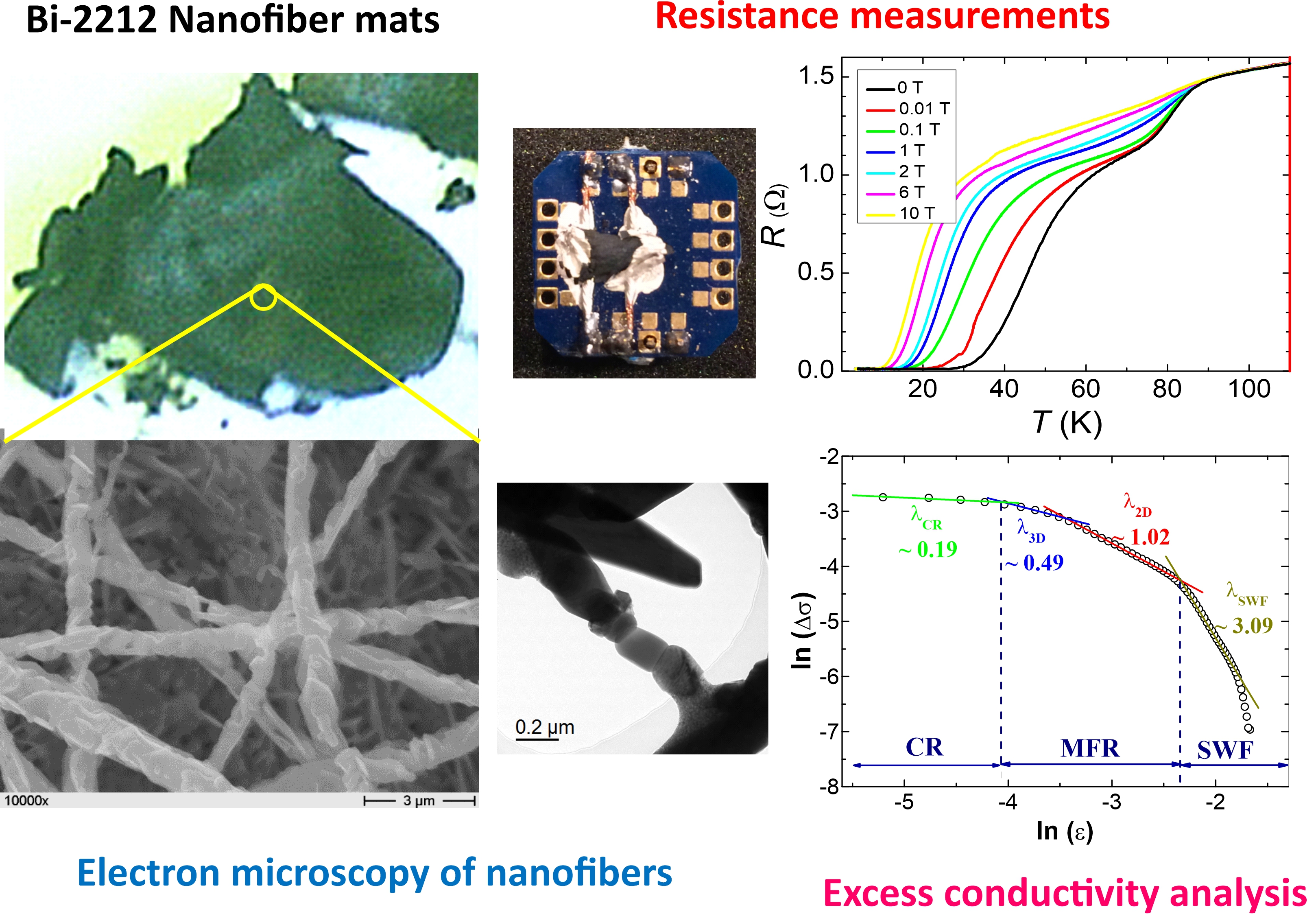
2.1. Sample Preparation

Nanowire networks of Bi-2212 system were made via the electrospinning procedure [15,18,21]. Acetate powders of various constituents with an initial composition of Bi:Sr:Ca:Cu = 1:1:1:2 as precursor material were mixed with polyvinyl pyrrolidone (PVP, MW = 1,300,000) dissolved in propionic acid. A mass ratio of 5:2 (acetates:PVP) was found to be optimal, and a mixture of 0.5222 g PVP in 5 mL propionic acid was used. This composition we will refer to as 1112-precursor. The parameters measured during the electrospinning process are given in the Supplementary Materials Table S1. After the electrospinning process, the resulting sample in the green stage looks like shown in Figure 1. A white fiber mat is obtained, which is very flexible and thus, can be shaped easily as discussed in Reference [26]. These polymer nanofibers contain the unreacted ceramic precursor material, finely distributed within each fiber. To obtain the superconducting material, a heat treatment is needed to eliminate the various organic materials from the green nanowires and finally, at the high temperature stage to develop the desired superconducting phase. The temperature program (see Figure 2) for the heat treatment was decided following the resuts of a differential scanning calorimetry (DSC) and thermogravimetric analysis (TGA) measurement as published in Reference [21]. As a final step, an oxygenation treatment in flowing pure O 2 ( T = 500 C) is required to compensate the oxygen loss and to obtain a properly superconducting phase.
The phase identification of the products was performed using a high-resolution automated RINT2200 X-ray powder diffractometer (XRD) operating at 40 kV and 40 mA (Cu-K α radiation). The products were found to be Bi-2212 phase with an insignificant amount of CuO stemming from the excess Cu in the precursor material, see also Figure S1 in the Supplementary Materials.

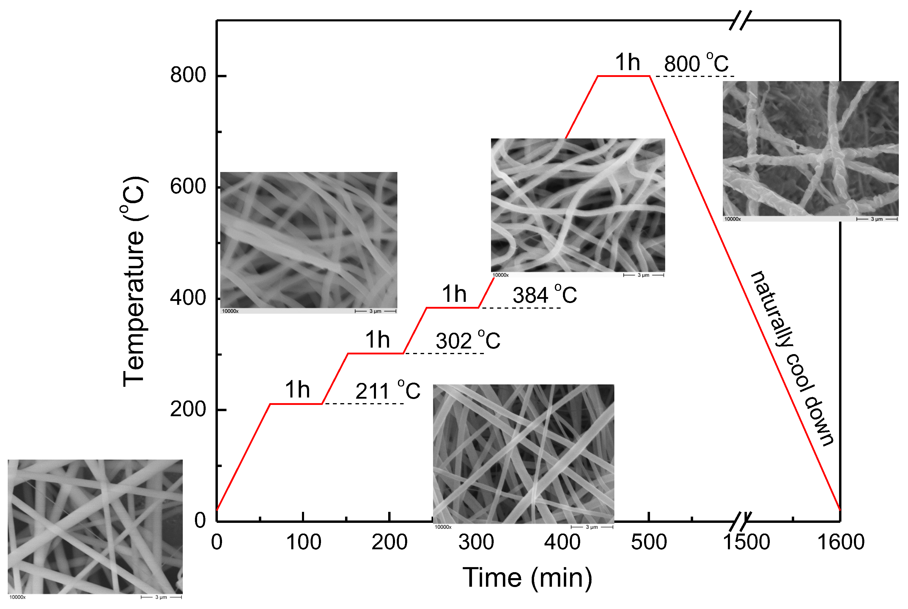
2.2. Resistance Measurements

Electric resistance measurements were done in the temperature interval of 3–300 K. A 10/12 T Teslatron cryostat (Oxford Instruments, UK) provided the magnetic field and the cryogenic environment for the sample using a variable-temperature insert. A quasi four-probe configuration was set up with two sides of the nanowire fabric covered with silver paint as the electrodes, and two contacts by gold wires on each electrode were fabricated in order to have a large distance between the voltage contacts. A 2.5 mA dc current was subjected perpendicularly to the direction of the magnetic field during the measurements. The sweep rate of magnetic field and the temperature steps were fixed as 0.7 T/min and 0.25 K, respectively. Details of these measurements were already reported in References [48,49,50].

2.3. Microscopy

Scanning electron microscopy micrographs were taken by a Hitachi S800 SEM microscope operating at 10 kV. EBSD investigations were implemented using a SEM microscope model JEOL 7000F with an additionally installed TSL analysis unit (TexSEM Labs, UT) [51]. The Kikuchi patterns were created at an acceleration voltage of 15 kV, and recorded by means of a DigiView camera system. A JEOL JSM-2011 TEM was used for the transmission electron microscopy (TEM) observations. Concerning TEM/EBSD/TKD analysis, some portions of the nanowire networks were dispersed in ethanol by ultrasonication. Very small amounts of this liquid were dropped on carbon coated TEM grids and then carefully dried to be used for SEM, EBSD, and TEM investigations [15,18]. This approach allowed to explore the more thinner nanowire regions, which permit the TKD transmission mode. No further treatment of the material surfaces was performed.
Related to the EBSD analysis, the TEM grid was fixed inside the SEM on a particularly constructed sample holder that allows to incline the sample by 70 accurately, which is needed for EBSD analysis. In the case of TKD, the platform with the sample holder is tilted by an angle of −20 . This allows, simultaneously with the sample mounting, the same position of the detector to be utilized for the EBSD detector as in the basic configuration. Now, the electron beam is transmitted across the sample and the cone of electrons is constructed on the backside of the sample. Additionally, the holder allows a second manner to operate EBSD in reflection mode, but using the TEM samples. This way of operation was used for the current nanowires not to be restricted to electron-beam-transparent sample sections. The electron beam performed at 30 kV, and the working distance was fixed at 5 mm. The step-size for EBSD analysis was selected to be 5 nm.
The TKD method allows, for the first time here, an appropriate investigation of the nanowires that are composed of nanometer-sized grains. Nevertheless, since the nanowires were mainly too thick for TKD, we conducted the EBSD analysis in reflection mode but utilizing the custom-constructed sample holder for TEM grids, which maintains the advantage of a small sample volume reducing the charging effects during the analysis.

3. Results and Discussion

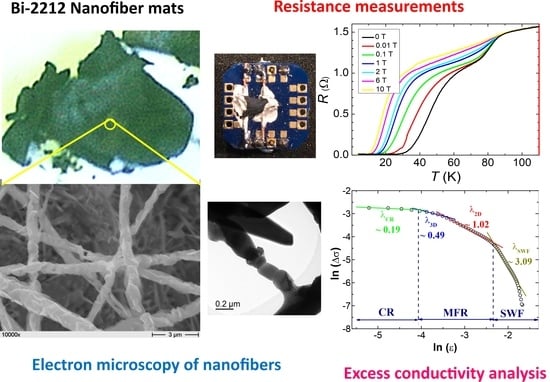
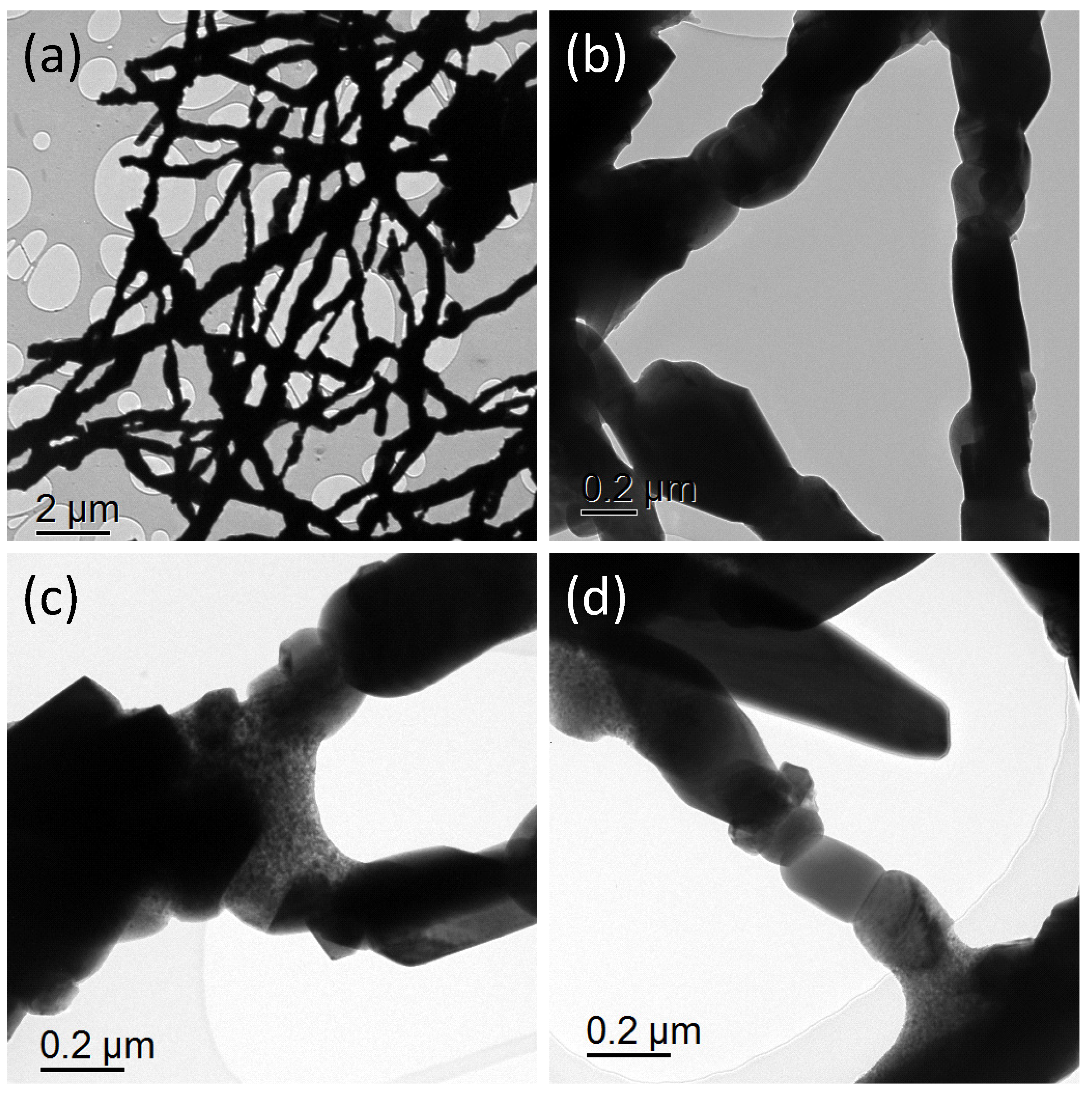
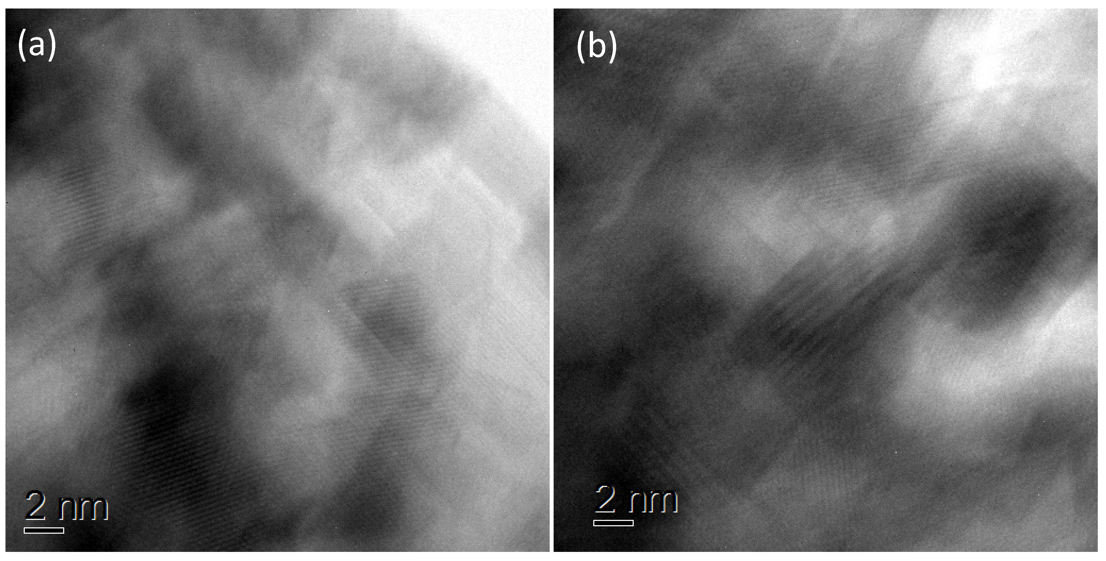
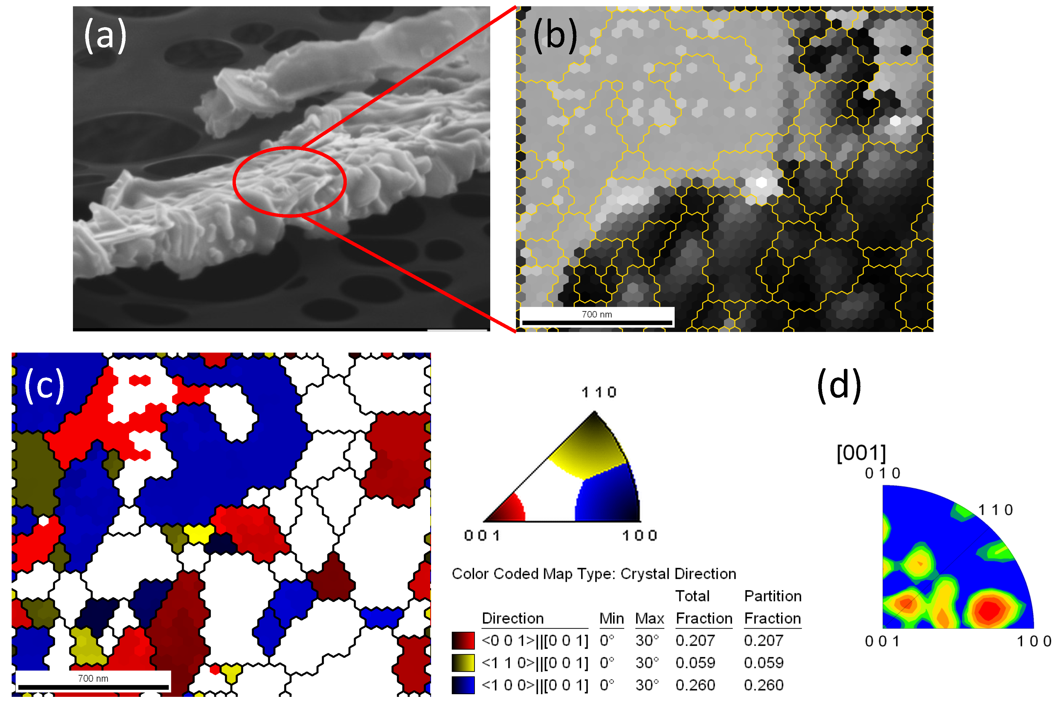
3.1. Microstructure of the Nanowire Network Fabrics

Figure 1a presents an as-spun (green) nanofiber mat. Note the size of the scale bar, which indicates that an upscaling to large-sized samples would be straightforwardly possible. Such large, thin superconductor samples can currently hardly be produced using any other method. This fiber mat is very flexible, and it can be cut and shaped at will. A demonstration of fabricating donut-shaped nanowire rings by wrapping the fabric around a wire has already been shown in Reference [26]. Figure 1b shows a SEM micrograph of the as-spun nanowires. The individual green nanowires are completely homogeneous. There are further numerous crossing points between the nanowires, but the nanowires are maximally touching each other. These interfaces or interconnects will later play an important role for the fully-reacted nanowires. In Figure 1c, a fully reacted Bi-2212 nanofiber mat sample is shown. The color is now fully black, and the resulting nanofiber mat is very brittle and easily separates into many flakes. A considerable shrinkage of the fiber mat is obvious from this image, even though still relatively large pieces can be obtained. This cracking of the material must be avoided when one aims for fabricating large superconducting fiber mats. A possible solution was discussed in Reference [52], forming a hybrid material of polymer and ceramic. Of course, such a hybrid material system would require to be adapted for low-temperature use.
In the present experimental stage, one can easily find large enough pieces for example, electric and magnetic characterization experiments. Finally, Figure 1d shows a low-magnification SEM image (1000×), which demonstrates that the length of the fully reacted nanowires can reach up to 100 μ m. A detailed statistics of the nanowire diameters was already presented in Reference [21].
In Figure 2, the temperature program applied to the as-spun nanofiber mat samples is presented. The temperature steps were chosen according to DSC/TGA analysis (see Reference [21]). The SEM images as insets to the graph give the various stages of the nanowire preparation. Starting from the as-spun nanowires, the temperature is increased to 211 C, where the PVP starts to decompose. At the next step of 302 C, the majority of the acetates convert to the corresponding oxides, and in a further step at 384 C the Bi-acetate decomposes and forms Bi 2 O 3 in air. Then, at a temperature of ∼800 C, the formation of the Bi-2212 phase occurs. The inset images show the removing of the organic material, and thus the size of the nanowires is gradually reducing. Finally, the last image presents the fully reacted Bi-2212 nanofibers. From the comparison of all images in Figure 2, it is evident that the size of the polymer nanofibers is shrinking before the chemical reaction sets in. As consequence, the thin polymer nanowires vanish completely. In fact, the relatively high required reaction temperature of Bi-2212 (∼800 C) poses a problem to maintain the nanowire shape. Thus, we have attempted to lower the reaction temperature by chemical additions as described in Reference [53], but for the prize of an inhomogeneous superconducting transition. In this sense, the present heat treatment conditions are the ones yielding the best superconducting properties.
Figure 3 illustrates two possibilities how the nanowire samples can be treated for further experiments. In Figure 3a, a nanowire section is presented sitting on top of a carbon-coated TEM-Cu-grid. Such a nanowire section maintains the presence of the interconnects between the individual nanowires for studying, especially for TEM investigations. Figure 3b presents nanowires on a Si/SiO 2 substrate. The nanowires adhere mechanically well to this surface, so it is possible to select nanowire sections for FIB-cutting and further treatments.
Figure 4a–d give TEM images of the fully-reacted Bi-2212 nanowires. Figure 4a presents a low-magnification image of a section with many interconnects. These interconnects are formed from the original polymer nanowires due to shrinkage effects which combine the formerly crossing nanowires into a solid structure. These interconnects are mechanically very stable as proven by the fact that such pieces have survived the ultrasonic treatment. From these images, we can see that the interconnects comprise often more than two nanowires at the same time, which provides many branching possibilities for the current flow through such a sample. Thus, these interconnects are very important for the flow of superconducting currents through the whole sample perimeter. Another consequence of this multiple branching of the currents is the paramagnetic response (PME) of some of the nanowire samples as discussed in Reference [54]. The Figure 4b,c show more details of the nanowires revealing the building-up of the nanowire. The grains are stacked together in a chain-like fashion, and some grains have grown out perpendicular to the main chain. The chains of the Bi-2212 grains can be as thin as a single grain, which directly explains the brittleness of the entire structure. Finally, Figure 4d shows such an extreme case where a nanowire is formed by a single Bi-2212 grain. Note that the grain boundaries within the nanowires seem to be relatively clean in contrast to the original expectation that some carbon-based material would be located at the GBs.
Figure 5a,b present high-resolution TEM images obtained on different thicker sections (see also the EBSD analysis of Figure 6) of the Bi-2212 nanowires. The fringes visible represent the Cu-O-planes, indicating the various orientations of the polycrystalline grain arrangement. The grain boundaries are only tiny sections, but the misorientation can be as high as 90 .
The TKD analysis of a nanowire section is finally shown in Figure 6a–d. Image (a) gives the nanowire section as SEM image taken in the conditions for EBSD (70 inclined to the electron beam). The red circle indicates the section analyzed by means of EBSD. Image (b) presents the image quality (IQ) map, which represents the image quality of the recorded Kikuchi patterns. Due to the stacking of the Bi-2212 grains, the image quality varies with position. In the image, the EBSD-detected grain boundaries are indicated using a yellow line. Image (c) shows the result in form of a crystal orientation (CO) map in (001) direction, that is, perpendicular to the sample surface. The length of the map corresponds to the TD direction, that is, the extension of the nanowire. The colors are given in this map according to each pole, and the remaining grains are plotted in white. From this mapping we learn that about half of the grains in this area do not have an orientation of 30 around the three poles, and the orientations around (001) and (100) dominate. Furthermore, the grains are typically elongated along their c-axis, being typical for the Bi-2212 grains with their long c-axis. More details on the EBSD/TKD analysis were already presented in Reference [55]. The misorientation of the GBs can be as high as 90 as was already observed in the TEM images. The majority of the GBs detected has misorientations at small angles (<5 ), but there is a considerable amount of large-angle GBs between 40 and 90 . The average grain diameter of the Bi-2212 grains was found to be ∼50 nm from TEM and EBSD. Finally, Figure 6d presents an inverse pole figure map. Here we can see that the grain orientation is not fully random, but certain orientations dominate. This indicates that there is an orientation of the Bi-2212 grains along the former direction of the polymer nanowire; that is, a fiber-like texture.

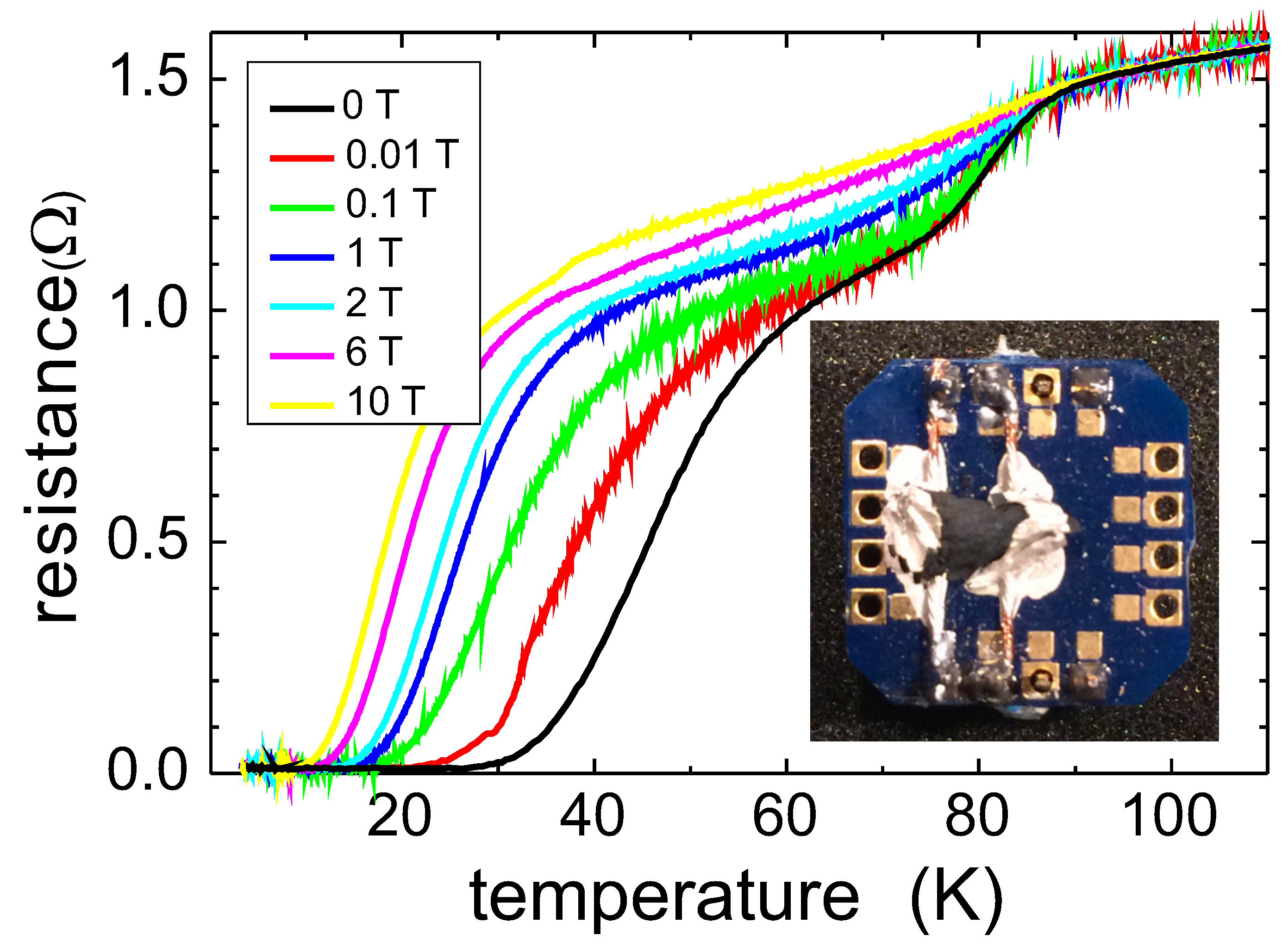
3.2. Resistance Measurements

Figure 7 presents the resistance measurement versus temperature for various applied magnetic fields. The applied current was 50 μ A. Two steps can be observed in the superconducting transition, and the superconducting transition is very broad, spanning more than 40 K, even in the case of no applied magnetic field. The typical rounding-off of the superconducting transition was explained in Reference [19] using the thermally-activated phase slip (TAPS) model [56], which could nicely be fit to the data. This model can, however, not be used at temperatures far below T c .
Due to the rounded-off shape of the superconducting transition, the onset temperature of superconductivity, T c , exp , were determined using the crosspoint of two linear fits to the data as described in previously in References [48,57]. T c , exp is found in this way at 76 K, which is distinctly below the bulk T c of 85 K [29]. This result was found to be consistent with field-cooling magnetization data in References [19,28]. The non-zero resistance in the interval of 40 K to 80 K (0 T-curve) is ascribed to the high normal state resistance R N due the intergrain weak-links within an individual Bi-2212 nanowire following Reference [19,58]. Here it is interesting to note that the onset temperature of the higher-T resistance drop decreases faster than the onset temperature of the lower-T resistance drop when increasing the external magnetic field. Here it is important to note that supercurrents can flow in the nanofiber mat samples even at applied magnetic fields of 10 T, which is a direct consequence of the numerous interconnects between the individual nanowires. The interconnects have thus a positive influence on the supercurrent flow as discussed in Reference [28].
In Figure 8, the analysis of the zero-field resistance curve is presented. The experimental data are indicated by black symbols ◯. The equation R ( T ) = R 0 + α ( T ) () can describe the metal-like behavior of the resisitvity in the normal state. Here, the α ( T ) describes the intrinsic electronic interaction and R 0 is determined by the defect density, impurities, heterogeneities in the sample. For the granular Bi-2212 nanowires, R 0 is high due the intergrain weak links within the individual nanowires. Furthermore, the resistance close to T = 4.2 K is low but not equal to zero, which is related to scattering of the charge carriers at the grain boundaries. The so determined normal state properties, R 0 and α , are listed in Table 1 below.
Important for the FIC analysis is the determination of the derivative d R / d T , which is shown in Figure 8 as a red line. Two distinct maxima of d R / d T are obtained which define the temperatures T c 1 and T c 2 . Here, we obtain T c 1 = 74.19 K and T c 2 = 44.37 K, which are distinctly lower than T c , exp = 76 K as determined above.
All the Bi-2212 nanofiber mat samples investigated have shown this double superconducting transition. As we can exclude any oxygen content variation due the nanoporous character of these samples, and also any secondary phase which would have been seen in the x-ray data, the second T c 2 must have an intrinsic origin. The value of T c 2 = 44.37 K, which is clearly smaller than the irreversibility temperature (66 K, 1 mT applied field) as seen in magnetic measurements [20,28], coincides very well with the 3D-2D transition observed in magnetization loops which takes place above 40 K [28]. This is further manifested by the size of the secondary transition being much larger as compared to the first transition at T c 1 . In the 3D-2D transition of Bi-2212 (and also in the Bi-2223 compound), the 3D vortices change to the characteristic 2D- or pancake vortices within the Cu-O-planes only. Below this transition, the flux pinning and the critical currents are comparable to that of the YBCO-based HTSc materials [59].

3.3. FIC Analysis

The excess conductivity ( Δ σ ) originated from the thermal fluctuations of the order parameter, Ψ , of HTSc systems is dependent on the internal and extrinsic properties (e.g., defects, morphology, etc.). Δ σ is determined experimentally as:
Δ σ = 1 ρ ( T ) 1 ρ n ( T ) ,
where ρ ( T ) are the experimental data of resistivity and ρ n ( T ) is the resistivity at the normal state. As for the Bi-2212 nanofiber mats studied here, the true cross section is unknown, we replace in the following ρ by the measured resistance, R.
According to the AL model [38,41,42], Δ σ above the mean-field temperature, T c (here, T c is the temperature at the maximum in d ρ / d T curves as shown in Figure 8), is expressed as Δ σ = A ϵ ( λ ) , where λ denotes the Gaussian critical exponent related with the conduction dimensionality D and ϵ = ( T T c ) / T c is the reduced temperature. The values of λ are 0.33 for dynamic fluctuations (CR), and 0.66 for static critical fluctuations, 0.5 for 3D fluctuations, 1.0 for 2D fluctuations, 1.5 for 1D fluctuations and finally, 3.0 for short-wave fluctuations. A is independent of temperature and is expressed as:
A = e 2 32 ξ c ( 0 ) ( 3 D ) , A = e 2 16 d ( 2 D ) , A = e 2 ξ c ( 0 ) 32 s ( 1 D ) ,
for the 3D-, 2D- and 1D-regimes, respectively. e is the electron charge, d is the effective layer thickness of the 2D system, ξ c ( 0 ) is the c-axis zero-temperature coherence length, and s is the wire cross-sectional area of the 1D system. The LD model predicts that the 2D to 3D transition happens at T LD temperature, which can be expressed in the following way:
T LD = T c ( 1 + E J ) ,
with E J = ( 2 ξ c ( 0 ) / d ) 2 denoting the Josephson coupling constant. The plot of ln ( Δ σ ) versus ln ( ϵ ) allows the determination of the various fluctuation regimes. The different regions of this plot are linearly fitted, and the values of the exponent λ are deduced from the slopes.
Figure 9 shows the result of the FIC analysis for the Bi-2212 nanofiber mat sample. Three main fluctuation regions, labelled CR (= critical region,), MFR (mean field region, consisting of the 2D- () and 3D- () regimes, and SWF (= short wave fluctuations,) are seen. The exponent values, the crossover temperatures, as well as the temperature width of the different regimes are listed in Table 1.
The regime occurred at high temperatures ( T c ) implies the end of GL approach, and the domination of the short-wave fluctuations. The effect of SWF appears when the coherence length order and the characteristic wavelength of the order parameter are in the same order [33,34]. On further reduction of the temperature, a MFR regime is appeared below T2D-SWF. It is well-known that undoped BSCCO systems (Bi-2212 and Bi-2223) show mostly 2D behavior. For this reason, the largest observed regime in the MFR region is the 2D fluctuation regime. Here, we have to note that no 1D fluctuation regime exists in the present Bi-2212 nanowire samples. The MFR regime extends to the crossover to the critical regime at a temperature T 3 D C R .
From the models of FIC, it is now possible to obtain several fundamental parameters of superconductivity. The thermodynamic critical field, B c ( 0 ) , and the Ginzburg number ( N G ) are related to each other via
N G = T G T c T c = 1 2 k B B c 2 ( 0 ) γ 2 ξ c 3 ( 0 ) ,
where k B denotes the Boltzmann constant, T G is the Ginzburg temperature and γ is the anisotropy parameter. From the knowledge of B c ( 0 ) , it is possible to determine the values of the critical fields, B c 1 ( 0 ) , B c 2 ( 0 ) and J c ( 0 ) using the relations
B c ( 0 ) = Φ 0 π 8 ξ c ( 0 ) λ ( 0 ) ,
B c 1 ( 0 ) = ln κ 2 κ B c ( 0 ) ,
B c 2 ( 0 ) = 2 κ B c ( 0 ) ,
J c ( 0 ) = 4 κ 3 3 ln κ λ ( 0 ) B c 1 ( 0 ) ,
where λ ( 0 ) is the London penetration depth, κ = λ / ξ is the Ginzburg-Landau parameter, and Φ 0 = h 2 e denotes the flux quantum, and e is the electron charge. For the anisotropy parameter γ , a value of 165 was used according to References [60,61]. All the superconducting parameters deduced from the FIC data are summarized in Table 1.

3.4. Discussion

The data determined by the FIC analysis give now some interesting input to understand the properties of the Bi-2212 nanofiber mat samples. Several types of Bi-2212 samples were already analyzed by means of excess conductivity/fluctuation-induced conductivity in the literature. This comprises single crystals [62] polycrystalline bulks [63,64,65], polycrystalline Bi-2212 doped with Ni, La [66,67,68], and Bi-2212 thin films [69]. Several authors found the missing 1D fluctuation regime in their Bi-2212 samples, and a similar observation was made when studying the Y-358 compound [70]. This is due to the strongly layered character of Bi-2212.
The crossover temperatures and the conductivity exponents determined for the Bi-2212 nanofibers correspond well to the theoretical numbers and to the previous results on polycrystalline samples, single crystals and thin films. The experimentally determined λ CR is close to the dynamic fluctuations.
The Josephson coupling constant E J is determined here to be 0.02567, which is similar to the data for polycrystalline, pure Bi-2223 [71], but considerably larger than that for Bi-2212 single crystals investigated by Mandal et al. [62]. This is a remarkable result, which was originally not expected (see Section 3.1). This further speaks for the performance of the nanofiber mats even in high applied fields. The Ginzburg number, N G , is found to be 0.02035, which falls in the typical range for HTSc materials.
The value of d (= effective length in the direction perpendicular to the current flow defining the effective layer thickness of the 2D-system) with 11.6 nm is smaller than that obtained in Reference [65] with 19 nm (polycrystalline Bi-2212 samples) and for Bi-2212 single crystals [62]. This may point to a squeezing of the Cu-O-layers, which is understandable when regarding the large surface contribution in the present nanometer-sized fibers (see also Figure S4 in the Supplementary Materials).
All values of the critical fields determined by the FIC analysis are reasonable for the Bi-2212 nanofiber mat samples, and the related current density, J c ( 0 ) , seems to be very small. This is, however, due to the low density of the nanofiber mats (0.74% of the theoretical density [28]) and the nanometer dimensions of the nanowires. The currents flowing inside the superconducting Bi-2212 grains are, of course comparable to those in other polycrystalline, bulk Bi-2212 samples.

4. Conclusions

To conclude, we have presented an analysis of the microstructure of Bi-2212 nanofiber mat samples and a study of excess conductivity (fluctuation-induced conductivity) in these samples. TEM and EBSD analysis of individual nanofibers revealed that the Bi-2212 grains within the individual nanowires are not randomly oriented, but do have a fiber-like texture, introduced by the original polymer nanowire. Furthermore, we found nanowire sections as thin as a single Bi-2212 grain. The numerous interconnects between the nanowires show a positive effect on the current flow, and are essential for the superconducting performance of the nanofiber mat samples. Resistance measurements were performed on the nanofiber mat samples to obtain the transition temperatures and the normal state resistivity. The present samples showed always a two-step superconducting transition. By means of the Aslamazov-Larkin model, the conductivity exponents and crossover temperatures and with them, several superconducting parameters could be extracted from the resistance measurements. The superconducting parameters obtained here for the Bi-2212 nanofiber mats coincide well with previous literature data on Bi-2212 and Bi-2223 materials. Remarkably, the Josephson coupling strength determined here is comparable to polycrystalline Bi-2223 samples, and thus much larger than that of single-crystalline Bi-2212. This manifests the good superconducting performance of the Bi-2212 nanofiber mats even in high applied magnetic fields.

Supplementary Materials

The following are available online at https://0-www-mdpi-com.brum.beds.ac.uk/2073-4352/10/11/986/s1, Table S1 (electrospinning parameters) and Figures S1–S4 (TEM images of the Bi-2212 nanofibers).

Author Contributions

Conceptualization, Methodology, M.R.K. and Y.S.; Investigation, Formal analysis, Y.S., M.R.K., A.K.-V., X.Z. and E.H.; Writing-original draft, writing-review and editing, M.R.K., A.K.-V. and Y.S.; Supervision, funding acquisition, M.R.K. All authors have read and agreed to the published version of the manuscript.

Funding

This work is subsidized by DFG project Ko2323/10, which is gratefully acknowledged.

Acknowledgments

We would like to thank T. Karwoth and A. Wiederhold (Saarland University, Saarbrücken, Germany) for experimental assistance.

Conflicts of Interest

The authors declare no conflict of interest.

References

  1. Bezryadin, A. Superconductivity in Nanowires; Wiley-VCH: Weinheim, Germany, 2013. [Google Scholar]
  2. Altomare, F.; Chang, A.M. One-Diemsional Superconductivity in Nanowires; Wiley-VCH: Weinheim, Germany, 2013. [Google Scholar]
  3. Dam, B.; Huijbregtse, J.M.; Klaasen, F.C.; van der Geest, R.C.F.; Doornbos, G.; Rector, J.H.; Testa, A.M.; Freisem, S.; Martinez, J.C.; Stäuble-Pümpin, B.; et al. Origin of high critical currents in YBa2Cu3O7−δ superconducting thin films. Nature 1999, 399, 439–442. [Google Scholar] [CrossRef] [Green Version]
  4. Awaji, S.; Suzuki, T.; Oguro, H.; Watanabe, K.; Matsumoto, K. Strain-controlled critical temperature in REBa2Cu3Oy-coated conductors. Sci. Rep. 2015, 5, 11156. [Google Scholar] [CrossRef] [PubMed] [Green Version]
  5. Li, D.; Xia, Y.N. Electrospinning of nanofibers: Reinventing the wheel? Adv. Mater. 2004, 16, 1151–1170. [Google Scholar] [CrossRef]
  6. Li, D.; McCann, J.T.; Xia, Y.N. Electrospinning: A simple and versatile technique for producing ceramic nanofibers and nanotubes. J. Am. Ceram. Soc. 2006, 89, 1861–1869. [Google Scholar] [CrossRef]
  7. Wu, H.; Pan, W.; Lin, D.; Li, H. Electrospinning of ceramic nanofibers: Fabrication, assembly and applications. J. Adv. Ceram. 2012, 1, 2–23. [Google Scholar] [CrossRef] [Green Version]
  8. Daristotle, J.L.; Behrens, A.M.; Sandler, A.D.; Kofinas, P. A review of the fundamental principles and applications of solution blow spinning. ACS Appl. Mater. Interf. 2016, 8, 34951–34963. [Google Scholar] [CrossRef] [Green Version]
  9. Cheng, B.; Tao, X.; Shi, L.; Yan, G.; Zhuang, X. Fabrication of ZrO2 ceramic fiber mats by solution blowing process. Ceram. Int. 2014, 40, 15013–15018. [Google Scholar] [CrossRef]
  10. Sharma, D.; Kumar, R.; Awana, V.P.S. DC and AC susceptibility study of sol-gel synthezied Bi2Sr2CaCu2O8+δ superconductor. Ceram. Int. 2013, 39, 1143–1152. [Google Scholar] [CrossRef]
  11. Deguchi, Y.; Kikuchi, H.; Mori, N.; Yamada, Y.; Atsumi, T.; Yoshida, K.; Ishibashi, T. Fluctuation-conductivity characterization of superconducting Bi2Sr2CaCu2O8+δ thinfilms prepared by the metal-organic decomposition method. Phys. Proc. 2013, 45, 193–196. [Google Scholar] [CrossRef] [Green Version]
  12. Lu, X.; Wang, T.; Qi, Y. Crystalline characteristics and superconducting properties of Bi2212 thin films by Pechini dol-gel method: Effect of heating rate on the film growth. J. Sol-Gel Sci. Technol. 2016, 77, 100–108. [Google Scholar] [CrossRef]
  13. Liu, X.; Zhao, G. One step preparation of photosensitive Bi2Sr2CaCu2O8+x films and their fine patterns by a photosensitive sol-gel method. Supercond. Sci. Technol. 2018, 31, 125017. [Google Scholar] [CrossRef]
  14. Reyntjens, S.; Puers, R. A review of focused-ion beam applications in microsystem technology. J. Micromech. Microeng. 2001, 11, 287–300. [Google Scholar] [CrossRef]
  15. Li, J.M.; Zeng, X.L.; Mo, A.D.; Xu, Z.A. Fabrication of cuprate superconducting La1.85Sr0.15CuO4 nanofibers by electrospinning and subsequent calcination in oxygen. CrystEngComm 2011, 13, 6964–6967. [Google Scholar] [CrossRef]
  16. Duarte, E.A.; Quintero, P.A.; Meisel, M.W.; Nino, J.C. Electrospinning of superconducting BSCCO nanowires. Physica C 2013, 495, 109–113. [Google Scholar] [CrossRef]
  17. Duarte, E.A.; Rudawski, N.G.; Quintero, P.A.; Meisel, M.W.; Nino, J.C. Electrospinning of superconducting YBCO nanowires. Supercond. Sci. Technol. 2015, 28, 015006. [Google Scholar] [CrossRef]
  18. Zeng, X.L.; Koblischka, M.R.; Hartmann, U. Synthesis and characterization of electrospun superconducting (La,Sr)CuO4 nanowires and nanoribbons. Mater. Res. Express 2015, 2, 095022. [Google Scholar] [CrossRef]
  19. Koblischka, M.R.; Zeng, X.L.; Karwoth, T.; Hauet, T.; Hartmann, U. Transport and magnetic measurements on Bi-2212 nanowire networks prepared via electrospinning. IEEE Trans. Appl. Supercond. 2016, 26, 1800605. [Google Scholar] [CrossRef] [Green Version]
  20. Koblischka, M.R.; Zeng, X.L.; Karwoth, T.; Hauet, T.; Hartmann, U. Magnetic properties of electrospun nonwoven superconducting fabrics. AIP Adv. 2016, 6, 035115. [Google Scholar] [CrossRef] [Green Version]
  21. Zeng, X.L.; Koblischka, M.R.; Karwoth, T.; Hauet, T.; Hartmann, U. Preparation of granular Bi-2212 nanowires by electrospinning. Supercond. Sci. Technol. 2017, 30, 035014. [Google Scholar] [CrossRef] [Green Version]
  22. Cena, C.R.; Torsoni, G.B.; Zadorosny, L.; Malmonge, L.F.; Carvalho, C.; Malmonge, J.A. BSCCO superconductor micro/nanofibers produced by solution blow spinning technique. Ceram Int. 2017, 43, 7663–7667. [Google Scholar] [CrossRef] [Green Version]
  23. Rotta, M.; Zadorosny, L.; Carvalho, C.L.; Malmonge, J.A.; Malmonge, I.F.; Zadorosny, R. YBCO ceramic nanofibers obtained by the new technique of solution blow spinning. Ceram. Int. 2016, 42, 16230–16234. [Google Scholar] [CrossRef] [Green Version]
  24. Rotta, M.; Motta, M.; Pessoa, A.L.; Carvalho, C.L.; Ortiz, W.A.; Zadorosny, R. Solution blow spinning control of morphology and production rate of complex superconducting YBa2Cu3O7−x nanowires. J. Mater. Sci. Mater. Electron. 2019, 30, 9045–9050. [Google Scholar] [CrossRef] [Green Version]
  25. Rotta, M.; Namburi, D.K.; Shi, Y.; Pessoa, A.L.; Carvalho, C.L.; Durrell, J.H.; Cardwell, D.A.; Zadorosny, R. Synthesis of Y2BaCuO5 nano-whiskers by a solution blow spinning technique and their successful introduction into single-grain, YBCO bulk superconductors. Ceram. Int. 2019, 45, 3948–3953. [Google Scholar] [CrossRef]
  26. Koblischka, M.R.; Koblischka-Veneva, A. Porous high-Tc superconductors and their applications. AIMS Mater. Sci. 2018, 5, 1199–1213. [Google Scholar] [CrossRef]
  27. Koblischka, M.R.; Koblischka-Veneva, A. The possible applications of superconducting nanowire networks. Mater. Today Proc. submitted.
  28. Zeng, X.L.; Karwoth, T.; Koblischka, M.R.; Hartmann, U.; Gokhfeld, D.; Chang, C.; Hauet, T. Analysis of magnetization loops of electrospun nonwoven superconducting fabrics. Phys. Rev. Mater. 2017, 1, 044802. [Google Scholar] [CrossRef] [Green Version]
  29. Mikheenko, P.N.; Uprety, K.K.; Dou, S.X. BSCCO. In Handbook of Superconducting Materials; Cardwell, D.A., Ginley, D.S., Eds.; IOP Publishing: Bristol, UK, 2003; Volume I. [Google Scholar]
  30. Kametani, F.; Jiang, J.; Matras, M.; Abraimov, D.; Hellstrom, E.E.; Larbalestier, D.C. Comparison of growth texture in round Bi2Sr2CaCu2O8 and flat Bi2Sr2Ca2Cu3O10 wires at its relation to high critical current density development. Sci. Rep. 2015, 5, 8285. [Google Scholar] [CrossRef] [PubMed]
  31. Oh, B.; Char, K.; Kent, A.D.; Naito, M.; Beasley, M.R.; Geballe, T.H.; Hammond, R.H.; Kapitulnik, A.; Graybeal, J.M. Upper critical field, fluctuation conductivity, and dimensionality of YBa2Cu3O7−x. Phys. Rev. B 1988, 37, 7861–7864. [Google Scholar] [CrossRef] [PubMed]
  32. Ghosh, A.K.; Bandyopadhyay, S.K.; Basu, A.N. Generalization of fluctuation induced conductivity in polyscrystalline Y1−xCaxBa2Cu3Oy and Bi2Sr2CaCu2O8+δ superconductors. J. Appl. Phys. 1999, 86, 3247–3252. [Google Scholar] [CrossRef]
  33. Fanfarillo, L.; Benfatto, L.; Caprara, S.; Castellani, C.; Grilli, M. Theory of fluctuation conductivity from interband pairing in pnictide superconductors. Phys. Rev. B 2009, 79, 172508. [Google Scholar] [CrossRef] [Green Version]
  34. Jurelo, A.R.; Costa, R.M.; Rodrigues Junior, P.; Serbena, F.C. Fluctuation conductivity and phase separation in polycrystalline Y1−xCexBa2Cu3O7−δ. J. Supercond. Novel Magn. 2010, 23, 247–252. [Google Scholar] [CrossRef]
  35. Roa-Rojas, J.; Costa, R.M.; Pureur, P.; Prieto, P. Pairing transition, coherence transition, and the irreversibility line in granular GdBa2Cu3O7−δ. Phys. Rev. B 2000, 61, 12457–12462. [Google Scholar] [CrossRef]
  36. Hannachi, E.; Slimani, Y.; Ben Salem, M.K.; Hamrita, A.; Al-Otaibi, A.L.; Almessiere, M.A.; Ben Salem, M.; Ben Azzouz, F. Fluctuation induced conductivity studies in YBa2Cu3Oy compound embedded by superconducting nano-particles Y-deficient YBa2Cu3Oy: Effect of silver inclusion. Indian J. Phys. 2016, 90, 1009–1018. [Google Scholar] [CrossRef]
  37. Almessiere, M.A.; Hannachi, E.; Slimani, Y.; Ghulam, Y.; Mumtaz, M.; Koblischka, M.R.; Koblischka-Veneva, A.; Manikandan, A.; Baykal, A. Dimensionality and superconducting parameters of YBa2Cu3O7−δ/(WO3 NPs)x composites deduced from excess conductivity analysis. Mater. Chem. Phys. 2020, 243, 122665. [Google Scholar] [CrossRef]
  38. Aslamazov, L.G.; Larkin, A.L. The influence of fluctuation pairing of electrons on the conductivity of normal metal. Phys. Lett. A 1968, 26, 238–252. [Google Scholar] [CrossRef]
  39. Lawrence, W.E.; Doniach, S. Proceedings of the 12th International Conference on Low Temperature Physics, Kyoto, Tokyo, Japan; Kanda, E., Ed.; Academic Press of Japan: Tokyo, Japan, 1971; p. 361. [Google Scholar]
  40. Maki, K.; Thompson, R.S. Fluctuation conductivity of high-Tc superconductors. Phys. Rev. B 1989, 39, 2767–2771. [Google Scholar] [CrossRef]
  41. Larkin, A.; Varlamov, A. Theory of Fluctuations in Superconductors; Oxford University Press: Oxford, UK, 2005. [Google Scholar]
  42. Litvinov, Y.V.; Vovk, R.V.; Dobrovolskiy, O.V. Evolution of excess conductivity in YBCO single crystals after irradiation with fast electrons. Physica C 2020, 573, 1353645. [Google Scholar] [CrossRef]
  43. Nayak, P.K.; Ravi, S. Excess conductivity and magneto-conductivity studies in pure and Ag-doped (La1−xYx)2Ba2CaCu5Oz superconductors. Supercond. Sci. Technol. 2006, 19, 1209–1214. [Google Scholar] [CrossRef]
  44. Humphreys, F.J. Characterization of fine-scale microstructures by electron backscatter diffraction (EBSD). Scr. Mater. 2004, 51, 771–776. [Google Scholar] [CrossRef]
  45. Trimby, P.W. Orientation mapping of nanostructured materials using transmission Kikuchi diffraction in the scanning electron microscope. Ultramicroscopy 2012, 120, 16–24. [Google Scholar] [CrossRef]
  46. Keller, R.; Geiss, R. Transmission EBSD from 10 nm domains in a scanning electron microscope. J. Microsc. 2012, 245, 245–251. [Google Scholar] [CrossRef]
  47. Sneddon, G.C.; Trimby, P.W.; Cairney, J.M. Transmission Kikuchi diffraction in a scanning electron microscope: A review. Mater. Sci. Eng. R 2016, 110, 1–12. [Google Scholar] [CrossRef]
  48. Karwoth, T. Electronic Transport Measurements on Electrospun High-Tc Fibers. Master’s Thesis, Saarland University, Saarbrücken, Germany, 2016. [Google Scholar]
  49. Karwoth, T.; Furutani, K.; Koblischka, M.R.; Zeng, X.L.; Wiederhold, A.; Muralidhar, M.; Murakami, M.; Hartmann, U. Electrotransport and magnetic measurements on bulk FeSe superconductors. J. Phys. Conf. Ser. 2018, 1054, 012018. [Google Scholar] [CrossRef]
  50. Karwoth, T.; Zeng, X.L.; Koblischka, M.R.; Hartmann, U.; Chang, C.; Hauet, T.; Li, J.M. Magnetoresistance and structural characterization of electrospun La1−xSrxMnO3 nanowire networks. Solid State Commun. 2019, 290, 37–41. [Google Scholar] [CrossRef]
  51. Orientation Imaging Microscopy (OIM Analysis™) Software Version V8.1; User Manual; EDAX Inc.: Draper, UT, USA, 2018.
  52. Frontera, P.; Kumita, M.; Malara, A.; Nishizawa, J.; Bonaccorsi, L. Manufacturing and assessment of electrospun PVP/TEOS microfibres for adsorptive heat transformers. Coatings 2019, 9, 443. [Google Scholar] [CrossRef] [Green Version]
  53. Zeng, X.L.; Koblischka, M.R.; Laurent, F.; Karwoth, T.; Koblischka-Veneva, A.; Hartmann, U.; Chang, C.; Kumar, P.; Eibl, O. Characterization of electrospun Bi2Sr2CaCu2O8+δ nanowires with reduced preparation temperature. IEEE Trans. Appl. Supercond. 2018, 28, 7200505. [Google Scholar] [CrossRef]
  54. Pessoa, A.L.; Koblischka-Veneva, A.; Carvalho, C.L.; Zadorosny, R.; Koblischka, M.R. Microstructure and paramagnetic Meissner effect of YBCO nanowire networks. J. Nanoparticle Res. in print.
  55. Koblischka-Veneva, A.; Koblischka, M.R.; Zeng, X.L.; Schmauch, J.; Hartmann, U. TEM and electron-backscatter analysis (EBSD) on superconducting nanowires. J. Phys. Conf. Ser. 2018, 1054, 012005. [Google Scholar] [CrossRef]
  56. Tinkham, M.; Lau, C.N. Quantum limit to phase coherence in thin superconducting wires. Appl. Phys. Lett. 2002, 80, 2946–2948. [Google Scholar] [CrossRef]
  57. Koblischka, M.R.; Roth, S.; Koblischka-Veneva, A.; Karwoth, T.; Wiederhold, A.; Zeng, X.L.; Fassoulas, S.; Murakami, M. Relation between Crystal Structure and Transition Temperature of Superconducting Metals and Alloys. Metals 2020, 10, 158. [Google Scholar] [CrossRef] [Green Version]
  58. Bollinger, A.T.; Rogachev, A.; Remeika, M.; Bezryadin, A. Effect of morphology on the superconductor-insulator transition in 1-dimensional nanowires. Phys. Rev. B 2004, 69, 180503. [Google Scholar] [CrossRef] [Green Version]
  59. Koblischka, M.R.; Sosnowski, J. Temperature-dependent scaling of pinning force data in Bi-based high-Tc superconductors. Eur. Phys. J. B 2005, 44, 277–280. [Google Scholar] [CrossRef]
  60. Musolino, N.; Bals, S.; van Tendeloo, G.; Clayton, N.; Walker, E.; Flükiger, R. Modulation-free phase in heavily Pb-doped (Bi,Pb)-2212 single crystals. Physica C 2003, 399, 1–7. [Google Scholar] [CrossRef]
  61. Clayton, N.; Musolino, N.; Giannini, E.; Garnier, V.; Flükiger, R. Growth and superconducting properties of Bi2Sr2Ca2Cu3O10 single crystals. Supercond. Sci. Technol. 2004, 17, S563–S567. [Google Scholar] [CrossRef]
  62. Mandal, P.; Poddar, A.; Das, A.N.; Ghosh, B.; Chaudhury, P. Excess conductivity and thermally activated dissipation studies in Bi2Sr2Ca1Cu2Ox single crystals. Physica C 1990, 169, 43–49. [Google Scholar] [CrossRef]
  63. Ghosh, A.K.; Basu, A.N. Fluctuation-induced conductivity in quenched and furnace-cooled Bi2Sr2CaCu2O8+δ: Aslamazov-Larkin or short-wavelength fluctuations. Phys. Rev. B 1999, 59, 11193–11196. [Google Scholar] [CrossRef]
  64. Ghosh, A.K.; Basu, A.N. Dimensional exponents of Gaussian and critical fluctuations in Bi2Sr2CaCu2O8+δ processed under different conditions. Supercond. Sci. Technol. 2000, 13, 343–348. [Google Scholar] [CrossRef]
  65. Ben Azzouz, F.; Zouaoui, M.; Annabi, M.; Ben Salem, M. Fluctuation conductivity analysis on the Bi-based superconductors processed under same conditions. Phys. Stat. Solidi 2006, 3, 3048–3051. [Google Scholar] [CrossRef]
  66. Harabor, A.; Rotaru, P.; Harabor, N.A. Effect of Ni substitute in off-stoichiometric Bi(Pb)-Sr-Ca-Cu(Ni)-O superconductor. Excess conductivity, XRD analysis and thermal behaviour. Ceram. Int. 2019, 45, 2742–2750. [Google Scholar] [CrossRef]
  67. Sedky, A.; Salah, A. Excess conductivity, diamagnetic transition and FTIR spectra of Ca substituted by La in (Bi.Pb):2212 superconducting system. J. Low Temp. Phys. 2020. [Google Scholar] [CrossRef]
  68. Khir, F.L.M.; Mohamed, Z.; Yusuf, A.A.; Yusof, M.I.M.; Yahya, A.K. Effect of Pb and Cr substitutions on phase formation and excess conductivity of Bi-2212 superconductor. AIP Conf. Proc. 2010, 1250, 500–503. [Google Scholar] [CrossRef]
  69. Marconi, D.; Pop, M.; Pop, A.V. Normal state resistivity and excess of conductivity around the optimal doping of Bi-2212 thin films. J. Alloys Compd. 2012, 513, 586–591. [Google Scholar] [CrossRef]
  70. Slimani, Y.; Hannachi, E.; Ben Salem, M.K.; Hamrita, A.; Ben Salem, M.; Ben Azzouz, F. Excess conductivity study in nano-CoFe2O4-added YBa2Cu3O7−δ and Y3Ba5Cu8O18±x superconductors. J. Supercond. Nov. Magn. 2015, 28, 3001–3010. [Google Scholar] [CrossRef]
  71. Oh, J.Y.; Le, T.M.; Pham, A.T.; Tran, D.H.; Yang, D.S.; Kang, B. Role of interlayer coupling in alkaline-substituted (Bi,Pb)-2223 superconductors. J. Alloys Compd. 2019, 804, 348–352. [Google Scholar] [CrossRef]
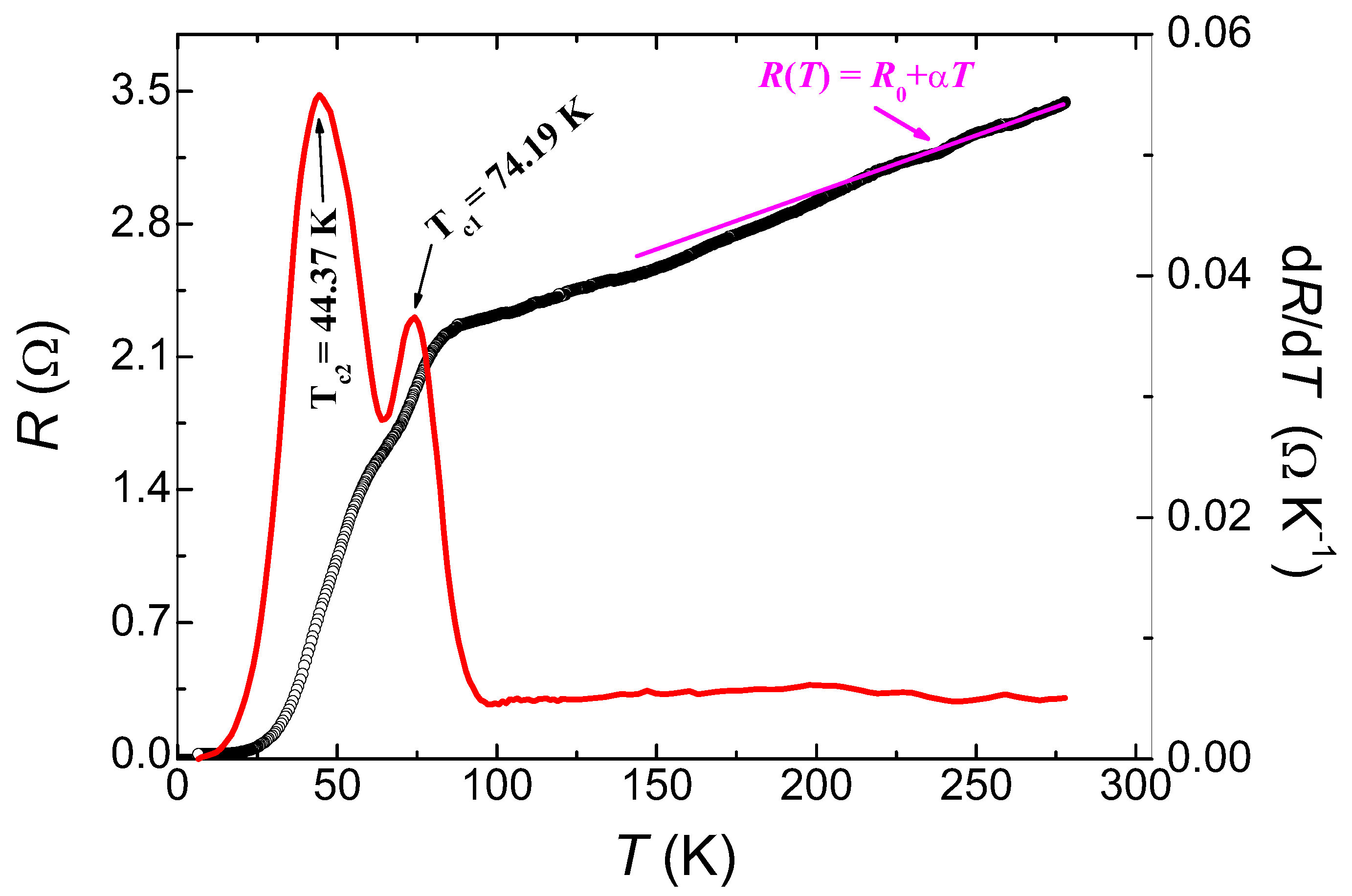
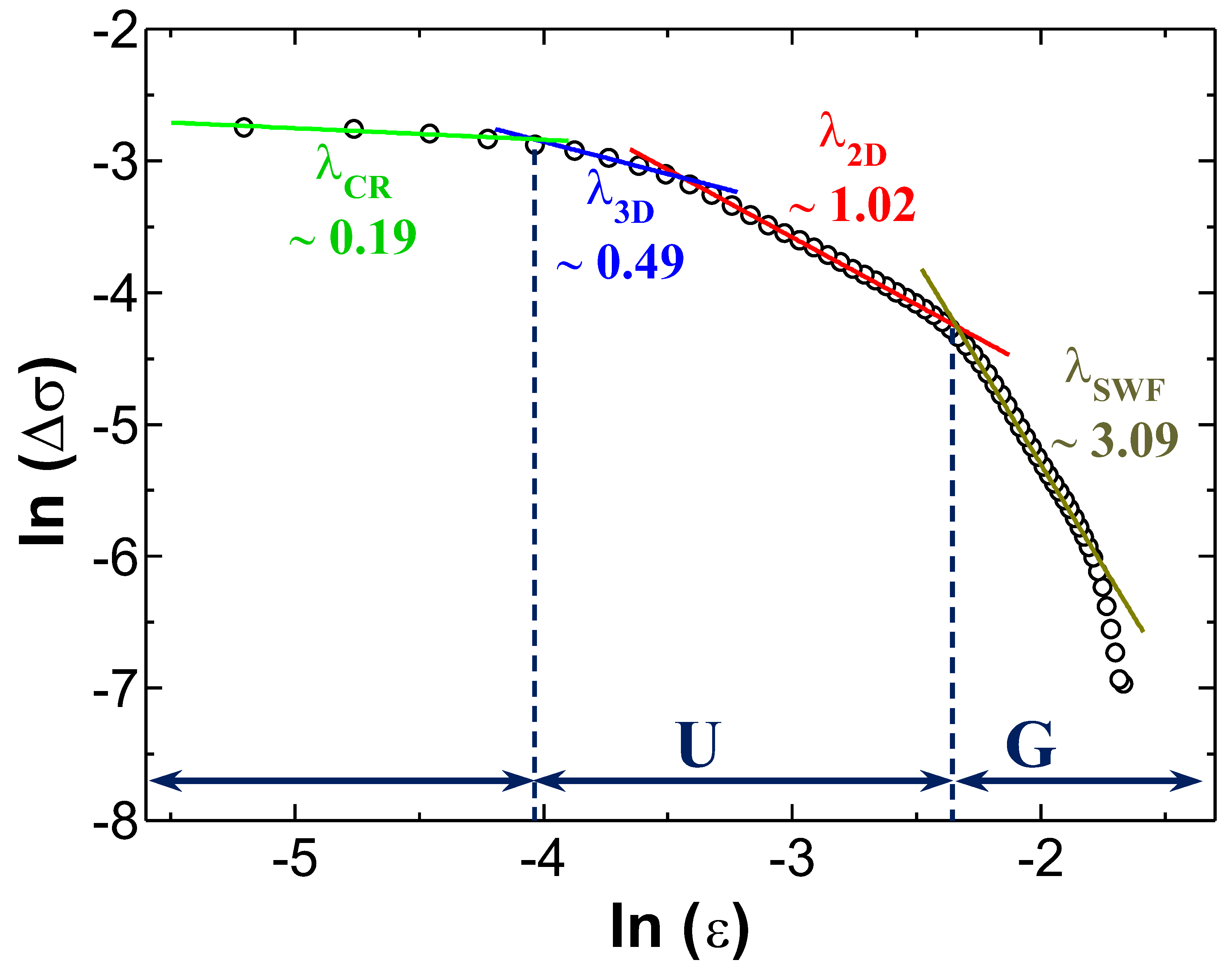
Figure 1. (a) As-spun (green) nanofiber mat after the electrospinning stage, (b) Scanning electron microscopy (SEM) image of the as-spun Bi-2212 nanowires, (c) fully reacted Bi-2212 nanofiber mat sample, and (d) SEM image of the fully reacted Bi-2212 nanowires.
Crystals 10 00986 g001
Figure 2. Heat treatment program of the Bi-2212 nanofiber mat samples. The inset SEM images (magnification 10,000×, scale bar 3 μ m) show the development of the ceramic nanofibers at each temperature step which was determined by differential scanning calorimetry (DSC)/thermogravimetric analysis (TGA). The shrinking of the nanowires in the temperature treatment is clearly visible.
Crystals 10 00986 g002
Figure 3. Two possibilities of handling the nanofiber mat pieces: (a) A broken-off section on a carbon-coated Cu-grid for transmission electron microscopy (TEM) imaging. This section maintains the interconnections between several nanowires. (b) Individual Bi-2212 nanowires on a silicon substrate. The nanowires adhere to the surface, so, e.g., FIB-cutting of sections becomes possible.
Crystals 10 00986 g003
Figure 4. TEM images of the Bi-2212 nanowires. (a) presents a low-magnification image of a section with many interconnects beteen the nanowires. (b,c) Details of the nanowires revealing the building-up of the nanowire. (d) shows a case where a nanowire is formed by a single Bi-2212 grain.
Crystals 10 00986 g004
Figure 5. (a,b) High-resolution TEM images of two different areas. The fringes indicate the orientation of the Cu-O-planes.
Crystals 10 00986 g005
Figure 6. Electron backscatter diffraction (EBSD) analysis within an individual nanowire. These images can be directly compared to the TEM images shown in Figure 4 and Figure 5. (a) gives a nanowire section in an SEM-image under 70 inclination. The area within the red circle is analyzed by EBSD. (b) shows an image-quality (IQ) map of the analyzed area, with the detected grains marked in yellow. (c) presents a crystal direction mapping in (001) direction, that is, the orientation is given perpendicular to the sample surface. The direction TD corresponds thus to the nanowire surface. The color code for the map is given on the right side; the grains not fitting to 30 around the poles are plotted in white. (d) shows the inverse pole figure in (001)-direction.
Crystals 10 00986 g006
Figure 7. Resistance as function of temperature for various applied magnetic fields (0–10 T). The inset gives an optical image of the nanofiber mat sample on the sample holder.
Crystals 10 00986 g007
Figure 8. Analysis of the resistance data at zero applied magnetic field. The experimental data are indicated by open circles (◯). The derivative, d R / d T (), shows peaks for two transitions at temperatures, T c 1 and T c 2 . The linear fit () to the data serves for the determination of α and R 0 .
Crystals 10 00986 g008
Figure 9. Fluctuation-induced conductivity (FIC) analysis plotting ln ( Δ σ ) vs. ln ( ϵ ) . Three main regimes can be identified (see main text), CR (), MFR and SWF (). The MFR regime comprises the 2D- () and 3D- () regimes. The dashed lines show the crossover temperatures, T LD and T 2 D SWF . The plot further indicates the conductivity exponents, see also Table 1.
Crystals 10 00986 g009
Table 1. Conductivity exponents, crossover temperatures, and superconducting parameters for the Bi-2212 nanowires.
NotationValues
Normal state parameters R 0 ( Ω )1.72 ± 0.01
α ( Ω · K 1 )6.2 × 10 2
Conductivity exponents λ CR 0.19 ± 0.02
λ 3 D 0.49 ± 0.04
λ 2 D 1.02 ± 0.05
λ SW 3.09 ± 0.1
Crossover temperatures T c 1 (K)74.19 ± 0.1
T c 2 (K)44.37 ± 0.1
T G (K)75.70 ± 0.1
T LD (K)76.59 ± 0.1
T 2 D SWF (K)81.35 ± 0.1
Superconducting parameters ξ c ( 0 ) (nm)0.93 ± 0.05
d (nm)11.68 ± 0.05
E J 0.0257
N G 0.0203
κ 151.7
B c 1 ( 0 ) (T)0.041 ± 0.002
B c 2 ( 0 ) (T)375.5 ± 0.2
J c ( 0 ) (A/cm 2 )671.1 ± 1
Publisher’s Note: MDPI stays neutral with regard to jurisdictional claims in published maps and institutional affiliations.

