Article

The Study on Structural and Photoelectric Properties of Zincblende InGaN via First Principles Calculation

1
College of Big Data and Information Engineering, Guizhou University, Guiyang 550025, China
2
Power Semiconductor Device Reliability Engineering Center of the Ministry of Education, Guiyang 550025, China
3
College of Information, Guizhou University of Finance and Economics, Guiyang 550025, China
4
College of Physics and Electronic Science, Guizhou Normal University, Guiyang 550025, China
*
Author to whom correspondence should be addressed.
Submission received: 7 November 2020 / Revised: 10 December 2020 / Accepted: 16 December 2020 / Published: 19 December 2020
(This article belongs to the Special Issue First-Principles SimulationNano-Theory)

Abstract

:
In this paper, the structure and photoelectric characteristics of zincblende InxGa1−xN alloys are systematically calculated and analyzed based on the density functional theory, including the lattice constant, band structure, distribution of electronic states, dielectric function, and absorption coefficient. The calculation results show that with the increase in x, the lattice constants and the supercell volume increase, whereas the bandgap tends to decrease, and InxGa1−xN alloys are direct band gap semiconductor materials. In addition, the imaginary part of the dielectric function and the absorption coefficient are found to redshift with the increase in indium composition, expanding the absorption range of visible light. By analyzing the lattice constants, polarization characteristics, and photoelectric properties of the InxGa1−xN systems, it is observed that zincblende InxGa1−xN can be used as an alternative material to replace the channel layer of wurtzite InxGa1−xN heterojunction high electron mobility transistor (HEMT) devices to achieve the manufacture of HEMT devices with higher power and higher frequency. In addition, it also provides a theoretical reference for the practical application of InxGa1−xN systems in optoelectronic devices.

Graphical Abstract

1. Introduction

GaN, as a representative of third-generation semiconductors with a wide bandgap, has numerous advantages, such as direct bandgap, high-temperature resistance, and easy formation of heterostructures. It has significant military and commercial value for meeting the working requirements of high-power, high-frequency, and anti-radiation semiconductor devices [1]. To further improve the performance of GaN and broaden its applications, an increasing amount of research has been published on the optoelectronic properties of doped GaN structures in experiments and theoretical calculations in recent years [2,3,4,5]. Studies have indicated a shift in focus towards InxGa1−xN alloys because they can be used as a candidate material for optoelectronic devices. This was illustrated by Lu, who prepared an ultraviolet detector that showed a good response in the ultraviolet 360–390 nm region, with a peak response rate of 0.15 A/W [6]. Furthermore, the band gap of InxGa1−xN alloys can continuously change from 0.7 to 3.4 eV with the change of x, which is almost perfectly matched to the solar spectrum. Taking this into account, InxGa1−xN alloys have now begun to attract widespread attention as new type of solar cell material [7,8,9,10,11,12].
For InxGa1−xN, the wurtzite structure is more stable than the zincblende structure. Furthermore, and it is difficult to achieve high-quality growth of zincblende structure. Thus, current research mainly focuses on the wurtzite structure. However, due to the strong polarization effect of the wurtzite structure, it is difficult to use zincblende InxGa1−xN to prepare enhanced mode high electron mobility transistor (HEMT) and high-reliability devices compared with the second-generation semiconductor materials, such as III–V compound semiconductors. In addition, the zincblende InxGa1−xN does not have spontaneous polarization, and its smaller effective mass of electrons at the minimum of the conduction band (CB) is beneficial in enhancing the frequency and power of the device [13,14,15]. Mullhauser used radio frequency plasma-assisted molecular beam epitaxy to grow zincblende In0.4Ga0.6N, of which the band gap was 2.46 eV [16]. Goldhahn studied the refractive index and energy gap of InxGa1−xN and suggested that the band gap bowing parameter of InxGa1−xN is different when the x is different [17]. In terms of theoretical research, a growing number of groups have conducted research on the band gap bowing parameter of zincblende InxGa1−xN [18,19,20,21,22,23,24], but few reports have been published that discuss in detail the lattice constant, the change of bandgap, density of state, and optical properties. These physical properties are relevant for InxGa1−xN alloy-based heterojunction electronic devices and optoelectronic devices. Furthermore, zincblende InxGa1−xN without the Stark effect helps to improve the luminescence efficiency of optoelectronic devices. Therefore, it is necessary to explore the zincblende InxGa1−xN.
In this paper, we calculate the basic physical properties of InxGa1−xN using the first principles, and analyzed the lattice constant, polarization characteristics, the change of bandgap, and optical characteristics. This could provide a theoretical reference for the experimental research of full-spectrum solar cells and HEMT devices with higher frequency and higher power.

2. Method of Calculation

The GaN crystal was confirmed with three stable phases, namely, zincblende, wurtzite, and rock salt structure. The zincblende GaN used in this paper belongs to cubic crystal (F 4 ¯ 3 M) space group; its lattice constant is a = b = c = 0.452 nm and the crystal angle is α = β = γ = 90° [25]. The structure used for calculation is a 2 × 1 × 1 supercell obtained by extending twice along the a-axis of the zincblende GaN primitive cell, which contains 8 nitrogen and 8 gallium atoms as shown in Figure 1a. Indium atoms are doped into the GaN bulk to replace the positions of gallium atoms to obtain ternary InxGa1−xN, where x is set as 0, 0.125, 0.25, 0.5, 0.75, and 1. To acquire the lattice mismatch of the close-packed planes of zincblende and wurtzite InxGa1−xN, we also calculate the lattice constants of wurtzite InxGa1−xN when x = 0, 0.125, 0.25, 0.5, 0.75, and 1; the calculated structures are shown in Figure 1b–g.
All calculations in this paper were completed using the Cambridge sequential total energy package (CASTEP) module in material studio 4.0 developed by Accelrys. In this calculation, when both the zincblende and wurtzite InxGa1−xN alloys were optimized. The Perdew–Burke–Ernzerhof (PBE) was chosen as the exchange-correlation function and the Broyden–Fletcher–Goldfarb–Shanno (BFGS) algorithm was adopted. The optimization parameters of the maximum interaction force between atoms, the convergence criterion of the maximum displacement, the maximum stress acting on each atom, and the self-consistent accuracy were set as: 0.01 eV/Å, 5.0 × 10⁻⁵ nm, 0.01 Gpa, and 5.0 × 10⁻⁶ eV, respectively. Because the calculation structures of zincblende and wurtzite InxGa1−xN are different, the setting of their energy cut-off and k-point density are different. For the zincblende InxGa1−xN, energy cut-off was set as 600 eV and k-point density was 3 × 6 × 6. For wurtzite InxGa1−xN, energy cut-off was set as 600 eV and the k-point densities were set as 4 × 4 × 5 for GaN, In0.125Ga0.875N, In0.25Ga0.75N and InN, and 8 × 8 × 2 for In0.5Ga0.5N and In0.75Ga0.25N.

3. Results and Discussion

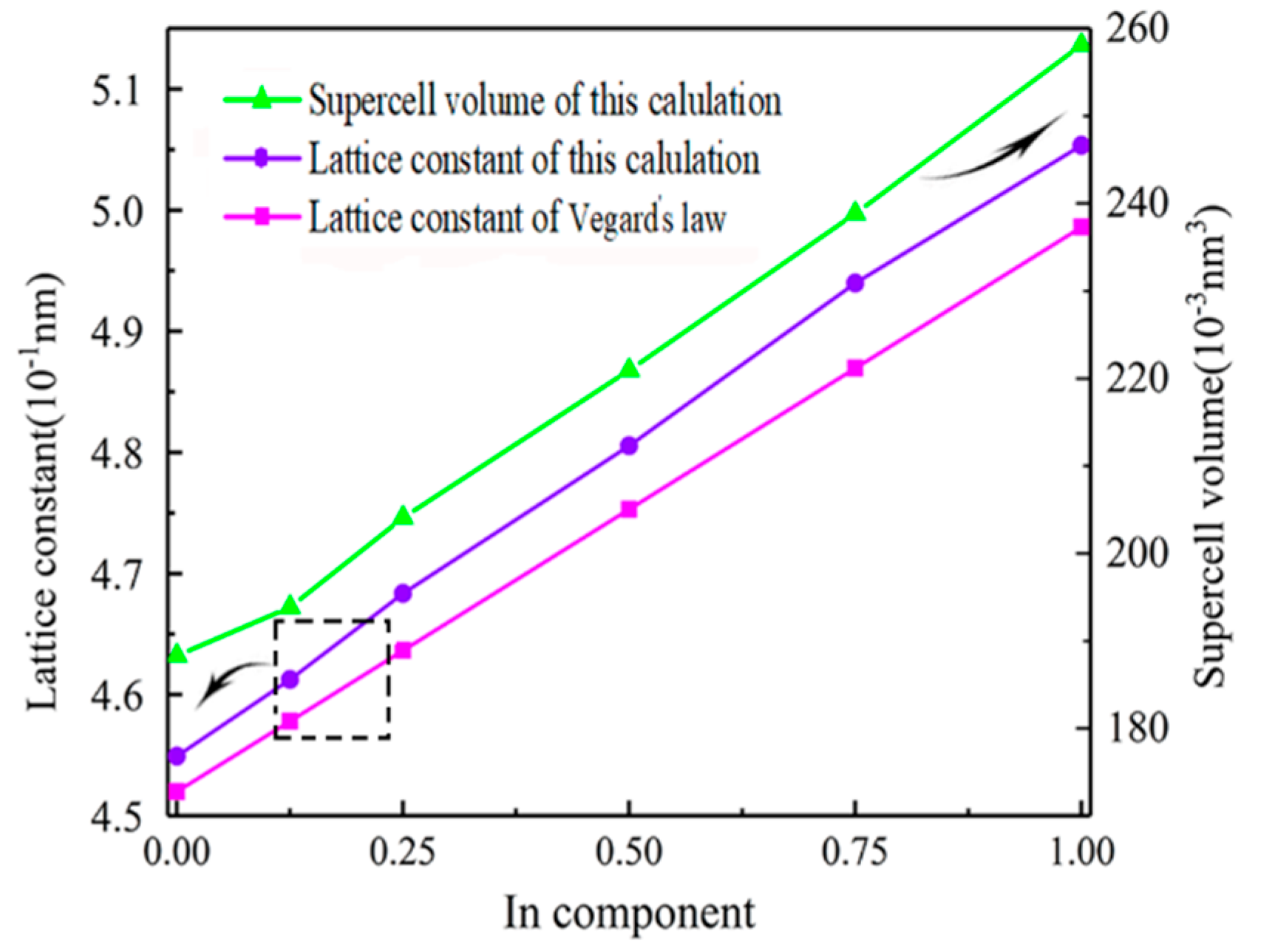
3.1. Lattice Constant

Figure 2 illustrates the optimized lattice constants and supercell volume of the zincblende InxGa1−xN when x is set as 0, 0.125, 0.25, 0.5, 0.75, and 1. The broken line formed by the green triangles in Figure 2 is the supercell volume of InxGa1−xN. It can be observed that the supercell volume of InxGa1−xN increases linearly with the increase in x, which is caused by the indium atomic radius being larger than that of gallium. The broken line formed by the magenta square points shows the lattice constants obtained according to Vegard’s law [26], which can be described via the following equation:
a I n x G a 1 x N = x a I n N + ( 1 + x ) a G a N
where a I n x G a 1 x N , a I n N , a G a N are the lattice constants of InxGa1−xN, InN, and GaN, respectively. The broken line formed by purple dots represents the optimized lattice constant of the zincblende InxGa1−xN systems. The optimized lattice constant of GaN is 0.4548 nm, which has an error of less than 1% from the experimental lattice constant value of GaN of 0.4520 nm [25]. For other InxGa1−xN structures, the errors between the calculated lattice constants of InxGa1−xN and Vegard’s law are less than 2%, which is related to the pseudopotential used in this calculation.
Figure 3 demonstrates the optimized lattice constants of the wurtzite InxGa1−xN. The blue, green, and orange curves are the a, c, and ideal axis c0 (c0 = 1.63a) lattice constants of InxGa1−xN, respectively, and all obviously increase with the increase in indium composition. The calculated lattice constants of wurtzite GaN are a = 0.323 nm, c = 0.525 nm, and c/a = 1.626; the differences between these calculated values and the experimental values are: 1.24%, 1.16%, and 0.062%, respectively [27]. In other indium compositions, the lattice constants that are calculated in this paper are consistent with those of the literature [28,29,30]. As evident from the illustration, the lattice constant c is different from the ideal lattice constant c0, leading to the spontaneous polarization of the wurtzite InxGa1−xN alloys. Moreover, the spontaneous polarization direction of wurtzite In0.5Ga0.5N is opposite to that of wurtzite GaN, In0.25Ga0.75N, In0.75Ga0.25N, and InN, because when indium composition is 0.5, c is greater than c0, and c is less than c0 for other indium compositions.
According to the definition of spontaneous polarization [31], we deduce the calculated equation of the spontaneous polarization intensity of wurtzite InxGa1−xN:
P S P = 4 3 e ( 1 4 a 2 + 1 3 c 2 ) ( 3 sin θ 1 )
sin θ = 3 k 2 4 3 k 2 + 4
k = c a
where θ is the angle between the bonds not parallel to c in the wurtzite InxGa1−xN and the plane formed by a 1 and   a 2 . The detailed derivation of spontaneous polarization in InxGa1−xN is described in the Supporting Information (SI).
According to Equations (2)–(4), the spontaneous polarization intensity PSP of wurtzite InxGa1−xN was calculated and the results are shown in Table 1. As shown, the spontaneous polarization intensity of wurtzite GaN is −0.030 C/m2, which only differs from the value in the literatures by −0.001 C/m2 [32,33]. The performance of wurtzite InxGa1−xN heterojunction HEMT devices is limited by the spontaneous polarization in wurtzite InxGa1−xN. Thus, replacing the wurtzite InxGa1−xN channel layer with nonpolarized zincblende InxGa1−xN is a potential choice. However, the difference in lattice constant between wurtzite and zincblende InxGa1−xN must be considered. Thus, we further calculated the close-packed plane lattice constants of the two structures, as shown in Table 1. The results show a negligible (0.23%) variation in lattice constants under all indium compositions. Hence, theoretically, the wurtzite InxGa1−xN channel layer can be replaced with zincblende InxGa1−xN without spontaneous polarization to further improve the performance of HEMT devices.

3.2. Band Structure

3.2.1. Correction of the Energy Gap

Figure 4 demonstrates the bandgap of the zincblende InxGa1−xN alloys with different indium compositions. The green curve in the figure shows the calculated bandgap; the bandgap of GaN is 1.536 eV, which is consistent with the value calculated by Mathieu Cesar et al. using PBE approximation [34]. Note that our calculated band gap of zincblende GaN is different from the 1.69 eV calculated by Poul Georg Moses et al. using PBE approximation [35], this may be due to the structure calculated by Poul Georg Moses et al. is wurtzite GaN structure, while the structure calculated in this paper is zincblende GaN. It is worth mentioning that the calculated band gap of GaN in this paper is smaller than the experimental value of 3.30 eV [12], this is because of the overestimation of the energy of the gallium d state in the calculation, leading to the enhanced interaction between gallium d and nitrogen p orbitals and resulting in broadening of the valence band (VB) [36]. Although this is a common phenomenon in the selection of GGA-PBE exchange-correlation functional calculations, the accurate calculation of the band gap is not important in trend analysis. To be specific, the main topic of this article concerns the same structural system and only changes the incorporation composition of indium [37,38]. Hence, the calculated series of band gaps are still comparable. To make the calculated band gaps of InxGa1−xN alloys closer to the experimental values, the calculated band gaps were corrected based on the experimental values of zincblende GaN and InN [12] using the correction formula as follows [38]:
E g , I n x G a 1 x N c o r = E g , I n x G a 1 x N c a l + x ( E g , I n N e x p E g , I n N c a l ) + ( 1 x ) ( E g , G a N e x p E g , G a N c a l )
where E g , I n x G a 1 x N c o r is the corrected band gap, E g , I n x G a 1 x N c a l , E g , I n N c a l , and E g , G a N c a l are the calculated band gaps of InxGa1−xN, InN, and GaN in this work, respectively; and E g , I n N e x p and E g , G a N e x p are the experimental band gaps of InN and GaN, respectively. The corrected results are shown by the curve composed of yellow triangles in Figure 4.
The modified band structures of the InxGa1−xN systems are plotted in Figure 5. The discussion of the energy band diagram is divided into the following points. (1) Type of band gap: According to Figure 5a, we conclude that GaN is a direct band gap semiconductor material; after the indium atoms are doped into GaN, the type of band gap of InxGa1−xN is still a direct gap, and the minimum of the CB and the maximum of the VB are located at the same Γ point in the Brillouin zone (BZ). (2) Degeneracy: Compared with Figure 5a,f, Figure 5 b–f shows an impurity energy level in both the CB and VB, increasing the degeneracy of InxGa1−xN. This is mainly due to the contribution of SP3 hybridization of gallium s/p and indium s/p orbitals. (3) Band gap: It can be clearly seen from Figure 4 that the band gap of InxGa1−xN decrease with the increase in x, which is caused by gallium s/p and indium s/p orbitals in the CB approaching the energy reference point as the indium compositions increase. In addition, it can be seen from Figure 5 that the band gaps of GaN and InN are 3.30 eV and 0.78 eV, respectively; hence, the band gap of InxGa1−xN alloys can continuously vary from 0.78 to 3.30 eV by adjusting the indium compositions. This is almost perfectly matched to the solar energy spectrum, and means that InxGa1−xN can be used to produce photovoltaic devices such as full-spectrum solar cells, by a combination of InxGa1−xN solar cells with various bandgaps.

3.2.2. Mechanism of Bandgap Reduction and Bandgap Bowing Parameter

From Figure 4 and Figure 5 it can be concluded that the band gap decreases with the increase in indium composition. To explore the cause of this phenomenon, the distribution of electron density difference of the InxGa1−xN systems was calculated, and the results are shown in Figure 6; blue indicates low electron density and red indicates high electron density. It can be seen from Figure 6b that when indium atoms replace the gallium atoms, there is an electron enrichment phenomenon around the indium atoms. This indicates that the indium has a stronger ability to bind electrons, which is due to the electronegativity of indium atoms being greater than that of gallium (according to Pauling’s rule, the electronegativities of gallium and indium are 1.6 and 1.7, respectively). Thus, more covalent bond components of indium–nitrogen and the ionic bond components decrease after indium atoms replace gallium. Furthermore, more covalent bond components of the SP3 hybrid bond of indium–nitrogen results in a smaller bond energy of indium–nitrogen compared with the gallium-nitrogen bond, thus, the band gap decreases with the increase in indium compositions.
The bandgap bowing parameter is integral in adjusting the energy gap of InxGa1−xN systems [35,39], therefore, here we discuss and analyze the value and origin of the bowing parameter. The relationship between the energy gap of the ternary alloy and the doping compositions can be expressed by the semi-empirical formula [40]:
E g , I n x G a 1 x N c o r = x E g , I n N e x p + ( 1 x ) E g , G a N e x p b x ( 1 x )
where b is the bandgap bowing parameter. We fitted the modified energy gap of the InxGa1−xN using Equation (3) and obtained b = 2.1 ± 0.14 eV as the average bowing parameter when the indium compositions are 0–1, which is caused by the volume deformation, structural relaxation, and charge exchange after the doping of indium atoms into the GaN system. The band gap bowing parameter obtained in this calculation is slightly different from the result in the literature, which is b = 1.9 ± 0.09 eV [19].

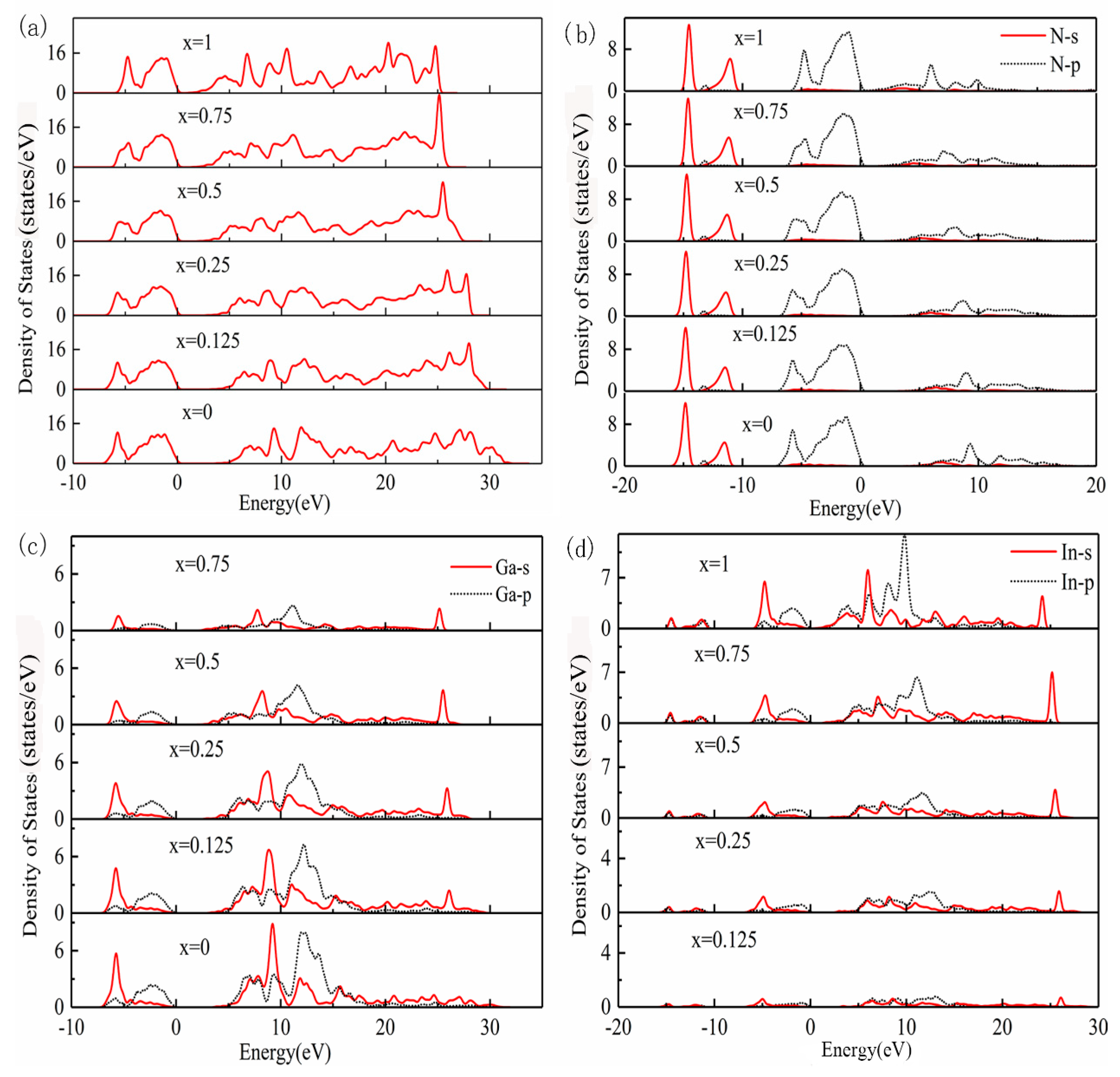
3.3. Density of States

Figure 7 shows the total density of states (TDOS) of zincblende InxGa1–xN and the partial density of states of indium, gallium, and nitrogen. Combining Figure 7b–d, the total density of states of Figure 7a is divided into three parts for discussion, namely: −10 to 5 eV, −5 to 0 eV, and CB. In the range of −10 to 5 eV, its main contribution comes from nitrogen p orbitals and gallium s orbitals. When the indium compositions in the InxGa1−xN systems increase, the electronic states of the gallium s orbitals decrease, while the electronic state of nitrogen p orbitals is almost unchanged, so the TDOS decreases in this range. The density of states in the energy range of −5 to 0 eV is mainly due to the contribution of the nitrogen p orbital and does not change with the increase in doping x. The TDOS in the CB is mainly affected by the SP3 hybridization of gallium s/p orbitals and indium s/p orbitals. Apparently, with the increase in indium compositions, gallium s/p orbitals and indium s/p orbitals move to lower energy, causing the TDOS of the CB to move to the energy reference point and the InxGa1−xN systems to undergo redshift, which is consistent with the conclusion of the band structure.

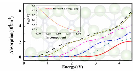
3.4. Optical Properties

Theoretically, the dielectric function can reflect the material’s response to electromagnetic signals and describe other optical parameters of the crystal. In the range of the linear response, the equations of the dielectric function are the following [41]:
ε ( ω ) = ε 1 ( ω ) + i ε 2 ( ω )
N ( ω ) = n ( ω ) + i k ( ω )
ε 1 = n 2 + k 2
ε 2 = 2 n k
where ε1 and ε2 are real and imaginary parts of the dielectric function, respectively, and n and k are refractive index and extinction coefficient, respectively. InxGa1−xN alloys are direct bandgap semiconductor materials, therefore, the dielectric function and absorption parameter α ( ω ) can be derived using the definition of the direct transition probability and the Kramers-Kronig relationship [42,43,44].
ε 1 ( ω ) = 1 + 2 e ε 0 m 2 V , C B Z 2 d K ( 2 π ) 3 | a M V , C ( K ) | 2 [ E C ( K ) E V ( K ) ] / 1 [ E C ( K ) E V ( K ) ] 2 / 2 ω 2
ε 2 ( ω ) = π ε 0 ( e m ω ) 2 V , C { B Z 2 d K ( 2 π ) 3 | a M V , C ( K ) | 2 δ [ E C ( K ) E V ( K ) ω ] }
α ( ω ) = 2 ω { [ ε 1 2 ( ω ) ε 2 2 ( ω ) ] 1 2 ε 1 ( ω ) } 1 2
where ε2 and λ0 are the dielectric constant and wavelength in vacuum, respectively, footnotes C and V represent the CB and VB, BZ is the Brillouin zone, K is the electronic wave vector, E C ( K ) and E V ( K ) are the intrinsic energy level of CB and VB, respectively, is the Planck constant, a is the unit vector of the vector potential A, and M V . C is transition matrix element.
We calculated the dielectric function of zincblende InxGa1−xN alloys when the indium compositions were changed to 0, 0.125, 0.25, 0.5, 0.75, and 1. The calculated results of the imaginary part ε2 of the dielectric function are shown in Figure 8. It is evident from the figure that the ε2 curve of GaN has three peaks, namely C1, C2, and C3, which are located near 8.4, 11, and 13 eV, respectively. Absorption peaks C2 and C3 are primarily caused by the transition of electrons in gallium s/p states to the unoccupied states. The absorption peak C1 reaches the maximum value, which is caused by the direct transition. It can be observed in the graph that the ε2 of InxGa1−xN alloys shift to low energy with the increase in indium atoms. This indicates that the electrons in the InxGa1−xN can undergo transitions even if they absorb photons with lower energy. Additionally, there is an absorption peak near 4 eV energy, which increases and moves to the lower energy direction with the increase in indium compositions. This may be due to the transition of indium s/p state electrons to the unoccupied state.
Figure 9 shows the absorption coefficient of InxGa1−xN alloys. There are four peaks, D1, D2, D3, and D4, in the absorption spectrum of GaN. Absorption peaks D1, D2, and D3 are located near 8, 11, and 13 eV, respectively. This is mainly due to the contribution of gallium s/p orbital electronic states. Therefore, the values of the three absorption peaks all decrease when the indium compositions increase. Another absorption peak D4 is located near 26 eV, whose main contribution comes from the gallium s orbital. However, when an indium atom is added, the influence of indium s/p orbitals is greater than that of the gallium s orbital. Hence, with the increase in indium compositions, the peak value increases. The absorption coefficient curve of InxGa1−xN alloys shifts in the low energy direction as x increases. This indicates that the doping of indium atoms improves the absorption of zincblende GaN for visible light, which is consistent with the result of the imaginary part of the dielectric function.

4. Conclusions

In this paper, the geometric parameters were optimized and the electronic structure and optical properties of zincblende InxGa1−xN (x = 0, 0.125, 0.25, 0.5, 0.75, 1) were calculated based on the density functional theory. The calculated results demonstrate that, after doping indium atoms, the nature of the direct bandgap of zincblende InxGa1−xN does not alter and the indium s/p electronic states are introduced near the energy reference point so that the bandgap decreases with the increase in x. By fitting the corrected bandgap, the average energy gap bowing parameter is obtained as b = 2.10 eV. Furthermore, as the indium compositions increases, the indium s/p and gallium s/p orbitals of the CB move to the energy reference point, resulting in a narrowing of the energy window in which electronic states cannot exist. In addition, the imaginary part of the dielectric function and the absorption coefficient of the InxGa1−xN structures shifts to low energy with the increase in x. This enhances the absorption of visible light and provides a theoretical reference for the application of InxGa1−xN alloys in the field of photovoltaic devices such as solar cells.

Author Contributions

Investigation, J.W.; Methodology, Z.H., J.L., X.G., Z.D. and J.W.; Software, X.L., E.L. and C.J.; Writing original draft, Z.L.; Writing review & editing, J.S. All authors have read and agreed to the published version of the manuscript.

Funding

This research was founded by the National Natural Science Foundation of China (Grant Nos. 11664005, 61564002); this research was also founded by the Science and Technology Foundation of Guizhou Province [2017] 1055.

Conflicts of Interest

The authors declare no conflict of interest.

References

  1. Park, S.H.; Chuang, S.L. Comparison of zinc-blende and wurtzite GaN semiconductors with spontaneous polarization and piezoelectric field effects. J. Appl. Phys. 2000, 87, 353–364. [Google Scholar] [CrossRef]
  2. Xia, S.; Liu, L.; Diao, Y.; Fend, S. Doping process of p-type GaN nanowires: A first principle study. J. Appl. Phys. 2017, 122, 135102. [Google Scholar] [CrossRef]
  3. Pan, F.C.; Yang, B.; Lin, X.L. The Study of Magnetism in Un-doped 3C-GaN: The First-Principles Calculations. J. Supercond. Nov. Magn 2015, 28, 1617. [Google Scholar] [CrossRef]
  4. Khan, M.J.I.; Liu, J.; Hussain, S.; Usmani, M.N. First Principle Study of Optical Properties of Cu doped zincblende GaN for Novel Optoelectronic Applications. Optik 2020, 208, 164529. [Google Scholar] [CrossRef]
  5. Li, J.; Liu, H.; Wu, L. The optical properties of GaN (001) surface modified by intrinsic defects from density functional theory calculation. Optik 2018, 154, 378. [Google Scholar] [CrossRef]
  6. Lu, Y.D.; Wang, L.W.; Zhang, Y. Properties of InGaN P-I-N ultraviolet detector. J. Semicond. Optoelectron. 2014, 35, 785. [Google Scholar]
  7. Kimura, R.; Shigemori, A.; Shike, J.; Ishida, K.; Takahashi, K. Improvement of cubic GaN film crystal quality by use of an AlN/GaN ordered alloy on GaAs (100) by plasma assisted molecular beam epitaxy. J. Cryst. Growth 2003, 251, 455. [Google Scholar] [CrossRef]
  8. Novikov, S.V.; Stanton, N.M.; Campion, R.P.; Morrist, R.D.; Kent, A.J. Growth and characterization of free-standing zinc-blende (cubic) GaN layers and substrates. Semicond. Sci. Technol. 2008, 23, 015018. [Google Scholar] [CrossRef]
  9. Liu, S.M.; Xiao, H.L.; Wang, Q.; Yan, J.D.; Zhan, X.M.; Gong, J.M.; Wang, X.L. InxGa1−xN/GaN Multiple Quantum Well Solar Cells with Conversion Efficiency of 3.77%. Chin. Phys. Lett. 2015, 32, 088401. [Google Scholar] [CrossRef]
  10. Jani, O.; Ferguson, I.; Honsberg, C.; Kurtz, S. Design and characterization of GaN/InGaN solar cells. Appl. Phys. Lett. 2007, 91, 132117. [Google Scholar]
  11. Neufeld, C.J.; Toledo, N.G.; Cruz, S.C.; Iza, M. High quantum efficiency InGaN/GaN solar cells with 2.95 eV band gap. Appl. Phys. Lett. 2008, 93, 1571. [Google Scholar] [CrossRef]
  12. Vurgaftman, I.; Meyer, J.R. Band parameters for nitrogen-containing semiconductors. J. Appl. Phys. 2003, 94, 3675. [Google Scholar] [CrossRef]
  13. Jia, W.L.; Zhou, M.; Wang, X.M.; Li, J.W. First-principles study on the optical properties of Fe-doped GaN. Chin. J. Phys. 2018, 67, 169. [Google Scholar]
  14. Lu, W. First-Principle Study of Electronic and Optical Properties of Wurtizite Structure GaN. Master’s Thesis, Xidian University, Xi’an, China, 2009. [Google Scholar]
  15. Shi, P. A Study on Transport Property of Cubic GaN Material and Its Heterojunction. Master’s Thesis, Xidian University, Xi’an, China, 2014. [Google Scholar]
  16. Mullhauser, J.R.; Brandt, O.; Trampert, A.; Jenichen, B.; Ploog, K.H. Green photoluminescence from cubic In0.4Ga0.6N grown by radio frequency plasma-assisted molecular beam epitaxy. Appl. Phys. Lett. 1998, 73, 1230. [Google Scholar] [CrossRef]
  17. Goldhahn, R.; Scheiner, J.; Shokhovets, S.; Frey, T.; Kohler, U.; As, D.J.; Lischka, K. Refractive index and gap energy of cubic InxGa1−xN. Appl. Phys. Lett. 2000, 76, 291. [Google Scholar] [CrossRef]
  18. Wright, A.F.; Nelson, J.S. Bowing parameters for zinc-blende AlxGa1−xN and InxGa1−xN. Appl. Phys. Lett. 1995, 66, 3051. [Google Scholar] [CrossRef]
  19. Kou, Y.K.; Liou, B.T.; Yen, S.H.; Chu, H.Y. Vegard’s law deviation in lattice constant and band gap bowing parameter of zincblende InxGa1−xN. Opt. Commun. 2004, 237, 363. [Google Scholar]
  20. Ferhat, M.; Furthmuller, J.; Bechstedt, F. Gap bowing and Stoke shift in InxGa1−xN alloys: First-principles studies. Appl. Phys. Lett. 2002, 80, 1394. [Google Scholar] [CrossRef]
  21. Camacho, D.L.A.; Hopper, R.H.; Lin, G.M.; Myers, B.S.; Chen, A.B. Theory of AlN, GaN, InN and their alloys. J. Cryst. Growth 1997, 178, 8. [Google Scholar]
  22. Wu, J.; Walukiewicz, W.; Yu, K.M.; Ager, J.W., III; Haller, E.E.; Lu, H.; Schaff, W.J. Small band gap bowing in InxGa1−xN alloys. Appl. Phys. Lett. 2002, 80, 4741. [Google Scholar] [CrossRef]
  23. Caetano, C.; Teles, L.K.; Marques, L.M.; Ferreira, L.G. Phase stability, chemical bonds, and gap bowing of InxGa1−xN alloys: Comparison between cubic and wurtzite structures. Phys. Rev. B 2006, 74, 5215. [Google Scholar] [CrossRef] [Green Version]
  24. Marques, M.; Teles, L.K.; Scolfaro, L.M.R.; Leite, J.R.; Bechstedt, F. Lattice parameter and energy band gap of cubic AlxGayIn1−x−yN quaternary alloys. Appl. Phys. Lett. 2003, 83, 890. [Google Scholar] [CrossRef]
  25. Dridi, Z.; Bouhafs, B.; Roterana, P. First-principles investigation of lattice constants and bowing parameters in wurtzite AlxGa1-xN and InxAl1−xN alloys. Semicond. Sci. Technol. 2003, 18, 850. [Google Scholar] [CrossRef]
  26. Lei, T.; Moustakas, T.D.; Graham, R.J.; He, Y.; Berkowitz, S.J. Epitaxial growth and characterization of zinc-blende gallium nitride on (001) silicon. J. Appl. Phys. 1992, 71, 4933. [Google Scholar] [CrossRef]
  27. Perlin, P.; Jauberthie-Carillon, C.; Itie, J.P.; San, M.A.; Grzegory, I.; Polian, A. Raman scattering and x-ray-absorption spectroscopy ingallium nitride under high pressure. Phys. Rev. B 1992, 45, 83. [Google Scholar] [CrossRef]
  28. Davydov, V.Y.; Klochikhin, A.A.; Emtsev, V.V.; Kurdyukov, D.A.; Ivanov, S.V. Band gap of hexagonal InN and InGaN alloys. Phys. Stat. Sol. (b) 2002, 234, 787. [Google Scholar] [CrossRef] [Green Version]
  29. Bungaro, C.; Rapcewicz, K. Ab initio phonon dispersions of wurtzite AlN, GaN, and InN. Phys. Rev. B 2000, 61, 6720. [Google Scholar] [CrossRef] [Green Version]
  30. Ruan, X.X.; Zhang, F.C. First-Principles Investigation on Electronic Structure and Optical Properties of Wurtzite InxGa1−xN Alloys. Rare Met. Mat. Eng. 2015, 44, 3027. [Google Scholar]
  31. Huang, K. Solid State Physics; Higher Education Press: Beijing, China, 1988; pp. 49–70. [Google Scholar]
  32. Bernardini, F.; Fiorentini, V.; Vanderbilt, D. Spontaneous polarization and piezoelectric constants of III-V nitrides. Phys. Rev. B 1997, 56, 10024–10027. [Google Scholar] [CrossRef] [Green Version]
  33. Hao, Y.; Zhang, J.F. Nitride Wide Band Gap Semiconductor Materials and Electronic, 3rd ed.; Science Press: Beijing, China, 2013; pp. 66–86. [Google Scholar]
  34. Cesar, M.; Ke, Y.Q.; Ji, W.; Gou, H.; Mi, Z.T. Band gap of InxGa1−xN: A first principles analysis. Appl. Phys. Lett. 2011, 98, 202107. [Google Scholar] [CrossRef]
  35. Moses, P.G.; Walle, C.G.V. Band bowing and band alignment in InGaN alloys. Appl. Phys. Lett. 2010, 96, 3675. [Google Scholar] [CrossRef]
  36. Li, J.B. First Principles Study of Electronic Structure and Optical Properties of GaN Doping. Ph.D. Thesis, Xidian University, Xi’an, China, 2019. [Google Scholar]
  37. Zhang, Y.; Shao, X.H.; Wang, Z.Q. A first principle study on p-type doped 3C-SiC. Acta Phys. Sin. 2010, 59, 5652. [Google Scholar]
  38. Zheng, S.W.; Fan, G.H.; Zhang, T.; Su, C.; Song, J.J.; Ding, B.B. First-principles study on the energy bandgap bowing parameter of wurtzite BexZn1−xO. Acta Phys. Sin. 2013, 62, 305. [Google Scholar]
  39. Moses, P.G.; Miao, M.; Yan, Q.; Walle, C.G.V. Hybrid functional investigations of band gaps and band alignments for AlN, GaN, InN, and InGaN. J. Chem. Phys. 2011, 134, 084703. [Google Scholar] [CrossRef]
  40. Hassan, F.E.H.; Hashemifar, S.J.; Akbarzadeh, H. Density functional study of Zn1−xMgxSeyTe1-y quaternary semiconductor alloys. Phys. Rev. B 2006, 73, 195202. [Google Scholar] [CrossRef]
  41. Zhang, Z.D.; Wang, Y.; Huang, Y.B.; Li, Z.H.; Yang, C. First principle study on the electronic and optical properties of AlxIn1−xAs. J. At. Mol. Phys. 2018, 36, 1057. [Google Scholar]
  42. Liu, X.F.; Luo, Z.J.; Zhou, X.; Wei, J.M.; Wang, Y.; Gou, X.; Lang, Q.Z.; Ding, Z. Calculation of electronic and optical properties of surface InxGa1−xP and indium-gradient structure on GaP (001). Comput. Mater. Sci. 2018, 153, 356. [Google Scholar] [CrossRef]
  43. Liu, X.F.; Ding, Z.; Lou, Z.J.; Zhou, X.; Wei, J.M.; Wang, Y.; Gou, X.; Lang, Q.Z. Theoretical study on the electronic and optical properties of bulk and surface (001) InxGa1−xAs. Physica B 2018, 537, 68. [Google Scholar] [CrossRef]
  44. Shen, X.C. Semiconductor Spectrum and Optical Properties, 2rd ed.; Science Press: Beijing, China, 2013; pp. 198–237. [Google Scholar]
Figure 1. Supercell structure of InxGa1−xN: (a) zincblende GaN structure of 2 × 1 × 1; (b) GaN structure of 2 × 2 × 1; (c) In0.125Ga0.875N structure of 2 × 2 × 1; (d) In0.25Ga0.75N structure of 2 × 2 × 1; (e) In0.5Ga0.5N structure of 1 × 1 × 2; (f) In0.75Ga0.25N structure of 1 × 1 × 2; (g) InN structure of 2 × 2 × 1. (From (b) to (g) is wurtzite InxGa1−xN alloys).
Crystals 10 01159 g001
Figure 2. The optimized lattice constants and volume of the zincblende InxGa1−xN systems.
Crystals 10 01159 g002
Figure 3. The optimized lattice constants of the wurtzite InxGa1−xN systems.
Crystals 10 01159 g003
Figure 4. The bandgap of zincblende InxGa1−xN systems as a function of indium compositions.
Crystals 10 01159 g004
Figure 5. Band structure of zincblende InxGa1−xN systems: (a) GaN; (b) In0.125Ga0.875N; (c) In0.25Ga0.75N; (d) In0.5Ga0.5N; (e) In0.75Ga0.25N; (f) InN.
Crystals 10 01159 g005
Figure 6. Distribution of electron density difference on the (111) plane of (a) GaN and (b) InxGa1−xN alloys.
Crystals 10 01159 g006
Figure 7. Density of states of InxGa1−xN alloys: (a) total density of states of InxGa1−xN alloys; (b) density of states of nitrogen s/p orbitals; (c) density of states of gallium s/p orbitals; (d) density of states of indium s/p orbitals.
Crystals 10 01159 g007
Figure 8. The imaginary part ε2 of the dielectric function of the InxGa1−xN alloys.
Crystals 10 01159 g008
Figure 9. The absorption coefficient of zincblende InxGa1−xN alloys.
Crystals 10 01159 g009
Table 1. Spontaneous polarization intensity of wurtzite InxGa1−xN (PSP), close-packed plane lattice constants of wurtzite and zincblende InxGa1−xN, and the difference (△L) in lattice constant of close-packed plane wurtzite and zincblende InxGa1−xN with different indium compositions.
Indium CompositionsPSP/(C/m2)Zincblende(nm)Wurtzite(nm)△L
0−0.030, −0.029 [32,33]0.32170.32290.12%
0.125−0.0310.32620.32740.12%
0.25−0.0090.32970.33090.12%
0.50.0370.33940.34010.07%
0.75−0.0110.34760.34990.23%
1−0.029, −0.032 [32,33]0.35730.35850.12%
Publisher’s Note: MDPI stays neutral with regard to jurisdictional claims in published maps and institutional affiliations.

