Article

Structural and Optical Properties of ZnO Thin Films Prepared by Molecular Precursor and Sol–Gel Methods

by
Theopolina Amakali
1,*,
Likius. S. Daniel
1,
Veikko Uahengo
1,
Nelson Y. Dzade
2,* and
Nora H. de Leeuw
2,3,*
1
Department of Chemistry and Biochemistry, University of Namibia, 340 Mandume Ndemufayo Avenue, Windhoek 9000, Namibia
2
School of Chemistry, Cardiff University, Main Building, Park Place, Cardiff CF10 3AT, UK
3
Department of Earth Sciences, Utrecht University, Princetonplein 8A, 3584 CB Utrecht, The Netherlands
*
Authors to whom correspondence should be addressed.
Submission received: 12 November 2019 / Revised: 17 February 2020 / Accepted: 18 February 2020 / Published: 22 February 2020
(This article belongs to the Special Issue Functional Oxide Based Thin-Film Materials)

Abstract

:
Zinc oxide (ZnO) is a versatile and inexpensive semiconductor with a wide direct band gap that has applicability in several scientific and technological fields. In this work, we report the synthesis of ZnO thin films via two simple and low-cost synthesis routes, i.e., the molecular precursor method (MPM) and the sol–gel method, which were deposited successfully on microscope glass substrates. The films were characterized for their structural and optical properties. X-ray diffraction (XRD) characterization showed that the ZnO films were highly c-axis (0 0 2) oriented, which is of interest for piezoelectric applications. The surface roughness derived from atomic force microscopy (AFM) analysis indicates that films prepared via MPM were relatively rough with an average roughness (Ra) of 2.73 nm compared to those prepared via the sol–gel method (Ra = 1.55 nm). Thin films prepared via MPM were more transparent than those prepared via the sol–gel method. The optical band gap of ZnO thin films obtained via the sol–gel method was 3.25 eV, which falls within the range found by other authors. However, there was a broadening of the optical band gap (3.75 eV) in thin films derived from MPM.

1. Introduction

Zinc oxide (ZnO) is one of the most widely researched semiconductor oxides, owing to its many versatile and attractive properties, such as high chemical and thermal stability, non-toxicity [1], ease of preparation, tunable direct wide band gap (3.4 eV), and high transparency in the visible region [2]. These properties saw ZnO thin films fabricated for various industrial applications, e.g., in optoelectronic devices [3], lasers, gas sensors, and ultraviolet (UV) light emitters [4], and as protective surface coatings [5]. ZnO plays important roles in a number of solar cell systems, such as silicon-based solar cells (first-generation), thin films (second generation), and organic multi-junction, dye-sensitized (third-generation) systems, either as a transparent conductive oxide (TCO) or as a junction for exciton separation [6].
Several techniques were proposed for the fabrication of ZnO thin films to modify its optical properties, including both physical and chemical processes. Physical methods include sputtering techniques [7,8,9], pulsed laser deposition [10], and molecular beam epitaxy (MBE) [11]. However, these methods are often complex and require costly vacuum equipment. In contrast, ZnO thin films can also be prepared via chemical methods, such as chemical bath deposition [12], chemical vapor deposition [13], atomic layer deposition [14], spray pyrolysis [15], printing [16], sol–gel spin coating [17], and electrochemical deposition [18], which are simpler methods and generally less costly. The conventional sol–gel method is often preferred over other chemical methods, due to its simplicity, lower crystallization temperature, and compositional control [19].
Structural and optical properties of ZnO thin films prepared via the sol–gel technique, using a variety of inorganic and organic precursors under different deposition conditions, were reported in the literature [20,21,22]. Post-heat treatment is one of the factors that plays a crucial role in the structural and optical properties of the ZnO thin films through the modification of their crystallinity and surface roughness. Thermal gravimetric and differential thermal gravimetric analysis (TGA/DTA) of ZnO gelatum by Meng et al. [23] showed that annealing the gel at 500 °C ensured complete removal of all the hydroxyl bonds and residues of organic matter. Chaitra et al. [24] investigated the role of annealing temperature (300, 400, and 500 °C) on the structural and optical properties of sol–gel-derived ZnO thin films. Thin films annealed at 500 °C showed tensile stress and a preferential orientation toward the (0 0 2) plane along the c- axis. Raoufi and Raoufi [25], using the same heat treatment conditions, obtained dense ZnO thin films with a (0 0 2) preferred orientation that was enhanced at 500 °C. Other authors reported similar observations [26,27]. In these studies, the authors reported that an increase in the annealing temperature reduced the full width at half-maximum (FWHM), increased grain size and crystallite size, and, as a result, increased the surface roughness. An increase in annealing temperature also decreased the optical band gap. However, cracking of the thin films during the annealing step remains a challenge, whereas the presence of interfaces within the thin films during drying can cause a reduction in the optical transparency [28]. It is, thus, important to explore other facile fabrication methods to overcome some of these challenges, and we, therefore, explored the fabrication of ZnO thin films using the molecular precursor method (MPM), which is a wet chemical process for the preparation of metal oxide thin films [29,30]. MPM, unlike the sol–gel method, is based on the use of metal complexes in coating solutions that are known to have excellent stability, homogeneity, and miscibility, owing to the metal complex anions which have better stability and can be dissolved in volatile solvents by combining them with the appropriate alkylamines [31].
The molecular precursor method (MPM) was employed successfully in the fabrication of copper oxides [31], as well as homogeneous and crack-free titania thin films [32]. Mashiyama and co-workers [33] reported the successful fabrication via MPM of Mg–Zn–O thin films, which exhibited good properties for applications as near-infrared UV-transparent electrodes for GaN-based UV-light-emitting diodes (LEDs). In 2012, Taka and co-authors [34] reported the use of MPM in the fabrication of composite ZnO thin films with dispersed Ag for application in GaInN blue LEDs. However, to the authors’ knowledge, to date, there are no reports on the fabrication and optical properties of pure ZnO thin films using the molecular precursor method.
In the present work, we report the growth of ZnO thin films on microscope slide substrates fabricated via the sol–gel method and MPM, as well as the investigation of their structural properties, surface morphology, and optical properties through X-ray diffraction (XRD), atomic force microscopy (AFM), and UV/visible light (Vis) spectra. Depending on the observed properties, the thin films thus fabricated could find application as sensors and catalysts, or in solar cells.

2. Materials and Synthesis Methods

2.1. Materials

Ethylenediaminetetraacetic acid (EDTA), zinc acetate dihydrate Zn(CH3COO)2.2H2O, 2-methoxyethanol, monoethalamine (MEA), absolute ethanol, and methanol were all purchased from Merck, Darmstadt, Germany. All reagents were of analytical grade and used without further purification. Microscope glass slides (26 mm × 38 mm) from B&C, Germany, were used as substrates for the deposition of ZnO thin films.

2.2. Synthesis of ZnO Thin Films

2.2.1. Preparation of Precursor Solution for Fabrication of ZnO Thin Film Using Sol–Gel Method

The Zn precursor solution (0.4 M) was prepared according to the procedure of Khan et al. [22] with modifications. The procedure used zinc acetate dihydrate, a 1:1 ethanol–methanol mixture, and dibutylamine as the Zn source, solvent, and stabilizer, respectively. The weight ratio of zinc acetate dihydrate to dibutylamine was fixed at 1.0. The solution was then stirred for 2 h at 50 °C and aged for 24 h at room temperature. This procedure yielded a light-yellow homogeneous viscous gel.

2.2.2. Preparation of Precursor Solution for Fabrication of ZnO Thin Films Using MPM

The procedure was based on the method of Sato et al. [29] with modifications. A Zn precursor solution (0.4 M) was prepared using EDTA, zinc acetate dihydrate, 2-methoxyethanol, and monoethanolamine as a complexing agent, Zn source, solvent, and stabilizer, respectively. The mole ratio of zinc acetate dihydrate to EDTA was 1:1, while it was 1:2.45 for monoethanolamine. In this procedure, EDTA was dissolved in 2-methoxyethanol and monoethanolamine was added; then, the solution was refluxed with constant stirring at 55 °C for 30 min. The solution was cooled to room temperature and zinc acetate dihydrate was added. The solution was refluxed further at 65 °C for 2 h, and a clear orange solution was obtained.

2.3. Film Fabrication by Coating and Heat Treatment

Firstly, 200 µL of the precursor solutions obtained from the MPM and the sol–gel routes were spin-coated onto pre-cleaned glass microscope slides using a double step mode, first at 500 rpm for 5 s and then at 2500 rpm for 30 s. The films were dried in a preheated oven at 150 °C for 10 min. The coating and drying steps were repeated up to 10 times to improve the thickness of the films. The thin films were then annealed at 500 °C for 1 h. Earlier studies demonstrated that annealing temperatures of around 500 °C generally result in the formation of well-crystallized metal-oxide thin films [20,21,22].

2.4. Characterization of ZnO Thin Films

The crystal structure of the fabricated ZnO thin films was investigated using a Bruker D8 Advance X-ray diffractometer (XRD) with CuKα radiation λ = 1.5402 . The surface morphology and topography were evaluated with a Bruker Dimension Edge atomic force microscope (AFM) with ScanAsyst TM and the Hitachi S4800 FE-SEM. The optical transmittance was measured on a Perkin-Elmer Lambda 750 UV-Vis/near-infrared (NIR) spectrophotometer in the range of 300 nm to 700 nm.

3. Results and Discussion

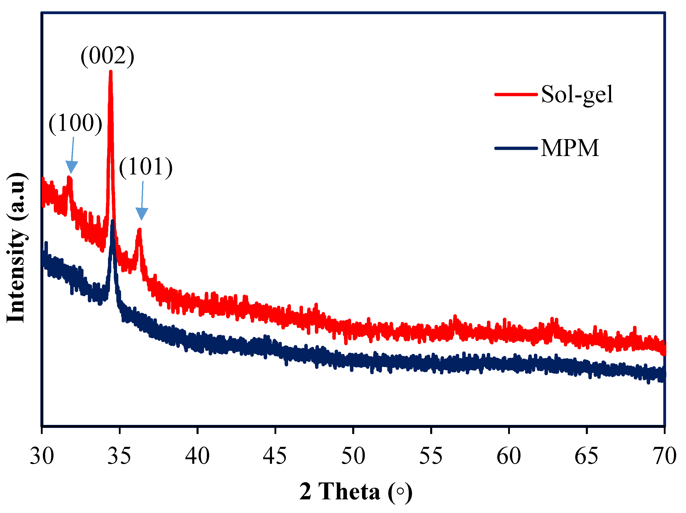
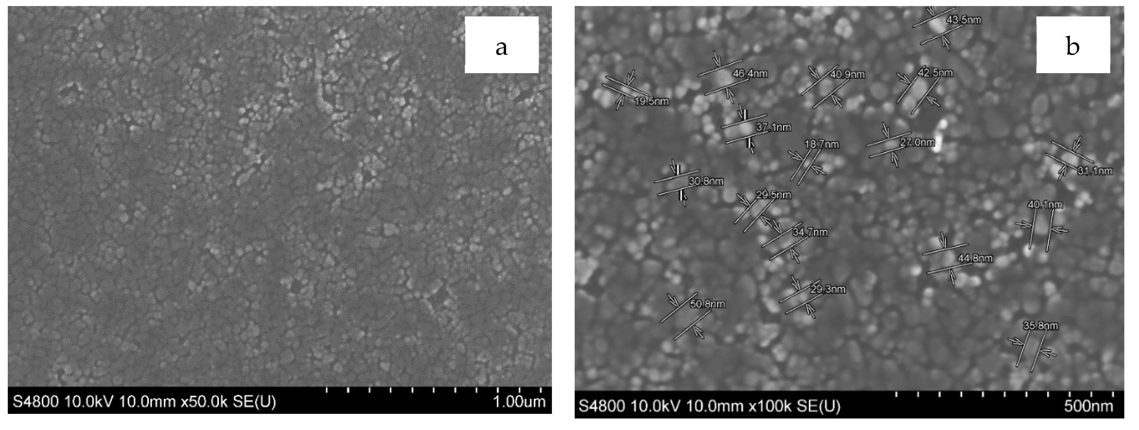
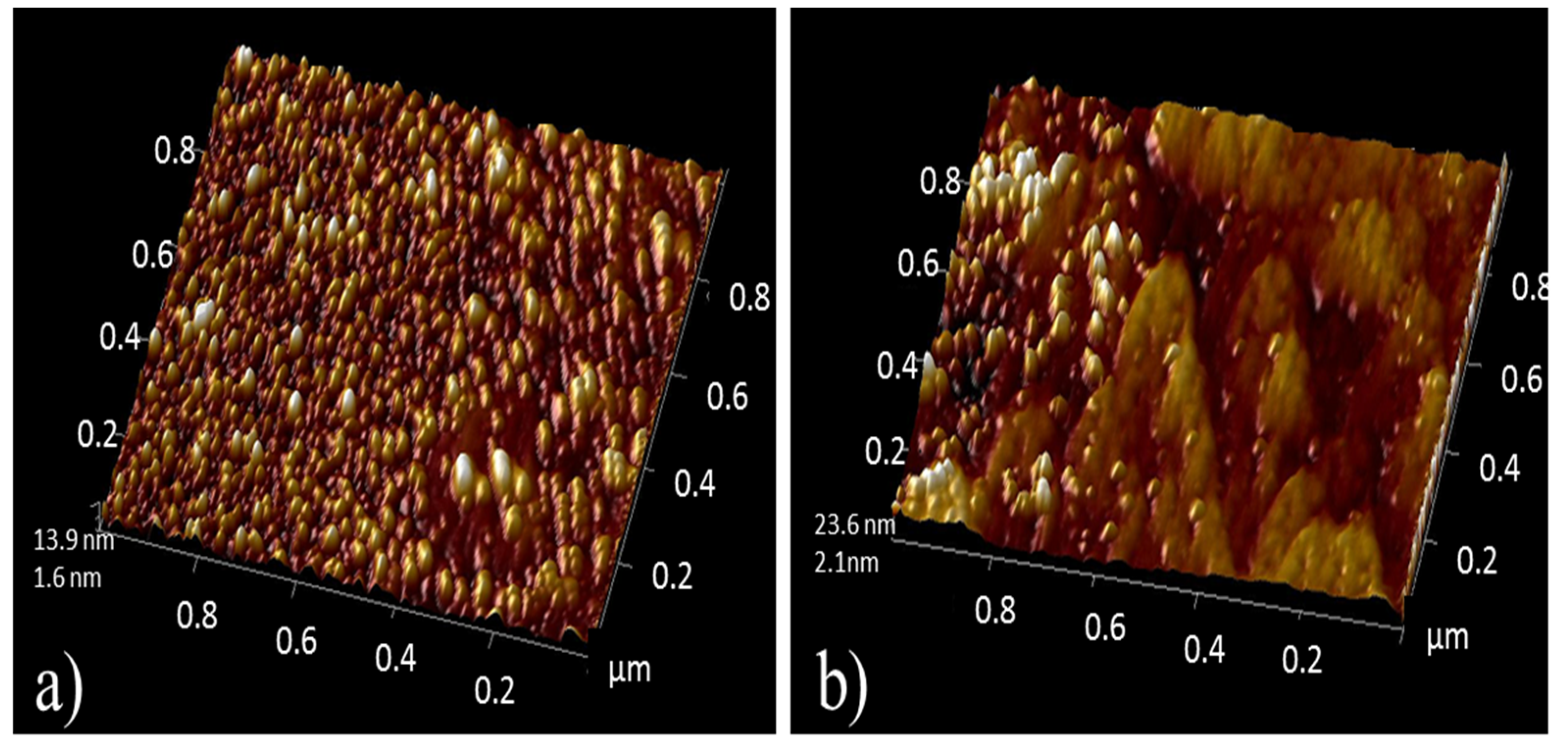
3.1. Crystal Structure and Particle Size

Figure 1 shows the XRD patterns of ZnO thin films on the microscope glass prepared via the MPM and sol–gel methods. The XRD spectra of sol–gel-derived thin films indicate the presence of three dominant peaks, corresponding to diffraction planes of (1 0 0), (0 0 2), and (1 0 1), showing the growth of ZnO crystallites along different directions. The peaks correspond to those of the standard ZnO (JCPDS 36-1451), and the typical hexagonal wurtzite structure was, therefore, inferred for the thin films from the XRD patterns. In this study, the baseline was not horizontal due to the amorphous glass substrate used. O’Brien et al. [26] observed a similar broad feature between 20° and 40°, which was attributed to the amorphous nature of the glass substrate used. Only the (0 0 2) peak was observed for the MPM-derived thin films, which is the kinetically favored orientation along the c-axis [35].
It was reported that, in ZnO, unlike thin films synthesized using short-chain alcohols such as ethanol, films synthesized using solvents with high boiling points (e.g., 2-methoxyethanol) show a very strong preferential orientation along the (0 0 2) plane [36,37,38]. This finding was attributed to the slow evaporation of high-molecular-weight alcohol upon heating, allowing structural orientation of the film before crystallization. In addition, this preferential orientation observed for ZnO grown on an amorphous glass substrate is due to the presence of non-bridging oxygen atoms in the glass substrate which assist the growth of ZnO along the (0 0 2) plane [39]. The (0 0 2) diffraction peak was widely observed as a preferred orientation in solution-grown ZnO [40,41], and the appearance of the (0 0 2) diffraction peak suggests that the surface free energy of this plane is the lowest both in the sol–gel- and in the MPM-fabricated ZnO thin films, thereby resulting in its preferred orientation.
The crystallite size (D) was estimated from the Debye–Scherrer equation.
D = 0.9 λ β c o s θ
where D is the crystallite size, λ (1.5418 nm) is the wavelength of the incident X-ray beam Cu K a , β is the full width at half-maximum, and θ is the Bragg diffraction angle. The evaluated structural parameters of the thin films synthesized via the two methods are presented in Table 1. The line broadening at half the maximum intensity (FWHM) was relatively large ( 4.535   × 10 3   r a d ) in thin films obtained from the MPM compared to those obtained from the sol–gel method ( 3.664 × 10 3 r a d ).
This indicates that crystallinity was better in the sol–gel-derived thin films, as the FWHM is inversely related to the crystallite size (Equation (1)). The crystallite size for the thin films synthesized through the MPM method was significantly smaller (32 nm) compared to that obtained through the sol–gel method (39.6 nm). A larger crystallite size of the sol–gel-derived ZnO thin films is an indication of less ordered grains and fewer micro-defects in the grains [39], which translates into a small value for the dislocation density and strain given in Table 1.
Figure 2 shows the scanning electron microscopy (SEM) image of a ZnO thin film synthesized via the molecular precursor method. The surface appears to be microporous with inhomogeneous spherical grains of different sizes. The average value of the crystallite size value obtained from the scanning electron microscopy (SEM) analysis was about 34 nm, which is quite close to that obtained from the XRD analysis (32 nm). Differences in thermal expansion represent one of the factors that affect the bonding between the coating and the underlying micro glass substrate. The influence of the difference in the thermal expansion coefficient between the ZnO film and the substrate is negligible, because of the very thin nature of the deposited ZnO thin film with a height of 7.67 nm (Figure 3). As a result, there is stable bonding between the ZnO thin film and the micro glass substrate. The exact bonding mechanism of the thin films and supportive substrate in the molecular precursor method is not clear. Further studies related to the observation of the interface between the coated ZnO thin film and glass substrate are needed.
Consistent with our results, previous reports showed that the molecular precursor method produces thin films of small crystallite size due to a rapid nucleation process [42]. The main difference between the sol–gel and the molecular precursor method is the absence of polymerization in the MPM solution, ensuring that the precursor film formed after coating remains amorphous and the solution remains stable over a long time [43]. The shrinkage rate and the packing of the precursor film on the substrate depend on the chain length of the alkylamine used in the synthesis [43]. It was suggested that the crystallite size of the metal oxide obtained via the MPM method will be smaller than that obtained from the sol–gel process [44], because the nucleation process in the sol–gel method during heat treatment is slower, as the polymeric chains rearrange to form the basic core structure of the metal oxide, resulting in relatively large crystallites.
The dislocation density ( δ ) and lattice strain ( ε ) in the thin films were estimated using the following equations:
δ = 1 D 2
ε = β c o s θ 4
As shown in Table 1, ZnO thin films obtained from the sol–gel method showed smaller values for the dislocation density and lattice strain than those obtained from the molecular precursor method. The dislocation density and lattice strain represent flaws and levels of defects in the crystal structure of the thin films, with smaller values indicating better crystallinity of the thin films [41]. Thus, it can be inferred that the thin films obtained from the sol–gel method are of better quality than those obtained from the molecular precursor method, potentially because the formation of crystallites of larger sizes allows the release of strain energy and relaxation between grains in the thin films [42].
Topographical features of the ZnO thin films were measured with AFM in tapping mode over a scan area of 1 µm2. Figure 3 shows the micrographs of the thin films prepared via the MPM and sol–gel methods. Based on the surface roughness and height recorded in Table 2, it is evident that the thin films obtained from MPM have a high surface roughness, with the root mean square (RMS) of the surface = 3.47 nm, compared to that obtained from the sol–gel method where RMS = 2.02 nm.
An inverse relationship between crystallite size and surface roughness was observed in this study, with the same findings reported by other authors [41]. It is, however, worth noting that the surface roughness of the ZnO thin film may also be affected by other factors and does not only depend on the crystallite size. Other parameters such as shape of the nanostructures, deposition conditions, and chemical reactions in the precursor solutions may also affect the surface roughness of ZnO thin films [43,44]. The influence of complexing agents on the grain size and surface roughness of ZnO thin films was described in detail by Nesheva et al. [39].

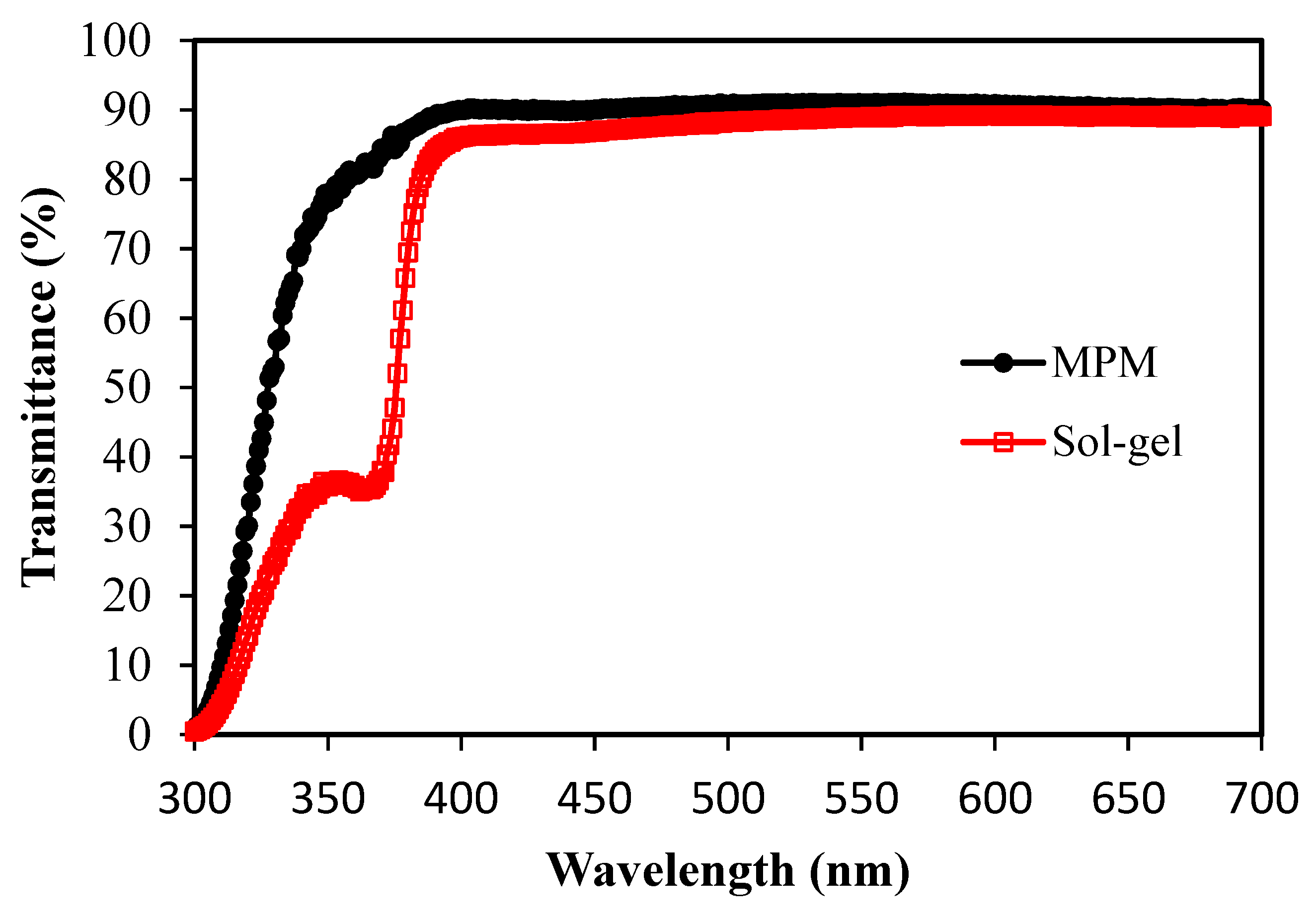
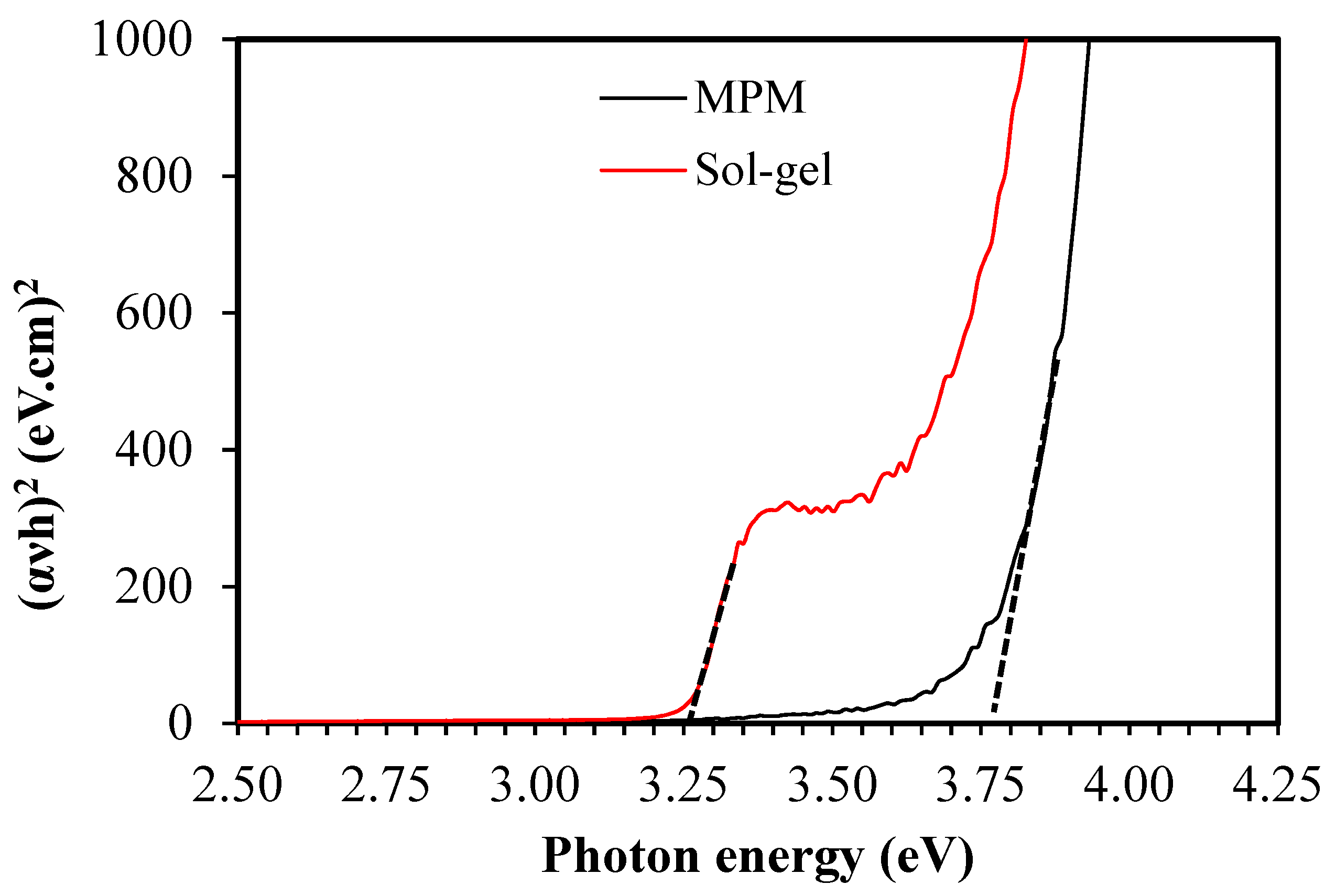
3.2. Optical Properties

Figure 4 shows the optical transmittance of the ZnO thin films synthesized via MPM and the sol–gel method. All transmittance spectra showed intensive absorption in the UV region, as expected for ZnO. The average transmittance for the ZnO thin films was calculated in the visible wavelength range of 400–700 nm. All thin films were highly transparent with an average transmittance of about 88% for the sol–gel-derived thin films and 90% for the MPM-derived thin films. Both films are, thus, suitable for optoelectronic devices, e.g., as window layers in solar cells. Salam et al. [45] determined the absorption edge of sol–gel-synthesized intrinsic (i-ZnO) and aluminum-doped zinc oxide (Al:ZnO) thin films mined to be at ~370 nm with ≥80% transmittance in the visible and near-infrared regions of the spectrum. Nearly 100% transmittance across the visible range was reported for ZnO thin films synthesized from a one-step spin-coating pyrolysis technique using zinc neodecanoate precursor [46]. A high transmittance (~92%) of ZnO nanowire arrays on indium tin oxide (ITO) substrate in the visible region was reported by Chen et al. [47]. The effect of annealing temperature on the structural, morphological, and optical properties of spray-pyrolized Al-doped ZnO thin films was systematically investigated by Kabir et al. [48]. It was shown that the annealing temperature affects the optical transmittance of the Al-doped ZnO thin films with the average transmittance value within the visible region found to be 70.3% for the as-deposited film [48].
The optical band gap energy (Eg) of the ZnO was determined from Tauc’s equation (Equation (4)) for direct band gap semiconductors.
Ahν = A(Eg)½,
where α is the absorption coefficient, hν is the incident photon energy, and A is a constant.
The optical band gap was then estimated by plotting (αhν)2 against the photon energy (h ν ) and extrapolating the linear portion of the curve to the photon energy axis, as shown in Figure 5. The presence of a single slope in the plot for ZnO fabricated using MPM suggests that, unlike in the sol–gel method, films in MPM have direct and allowed transitions. The band gap energy (eV) is obtained by extrapolating the straight-line portion of the plot to the zero absorption coefficient. Thus, the band gap values of the ZnO thin films fabricated via the sol–gel method and MPM were found to be 3.25 and 3.75 eV, respectively. However, the Tauc plot for thin films obtained from the sol–gel method shows a second linear segment, which could be due to sub-band gaps from a possible secondary phase [49]. The value of the optical band gap for the ZnO fabricated via the sol–gel method agrees with what is reported in the literature [50,51]. ZnO thin films that can absorb in the visible range of the spectrum make these materials suitable as a window layer in solar cells. However, the band gap for the ZnO thin film fabricated using MPM was a bit higher. There are two possible reasons for a large band gap value of the film: (i) owing to an axial strain effect from lattice deformation as suggested for ZnO films [52], or (ii) owing to a change in the density of semiconductor carriers. Which of these scenarios is the most likely, however, requires further investigation. Large optical band gap values (3.52–3.71 eV) were also reported by Akhtar et al. [53] and Wahab et al. [54]. Both groups attributed the blue shift of the band gap to residual strain defect and grain size confinement, although the grain sizes ranged between 28 nm and 150 nm. Samanta et al. [55] reported that the confinement regime of ZnO is much stronger when the particle size is much closer to the Bohr radius (2.3 nm). Hence, band gap broadening of ZnO thin films cannot be due to a quantum confinement effect, because the size of the ZnO crystallites is outside the quantum confinement regime, which is usually from 2 nm to 10 nm.
Given that the thin films in this study were very thin, the blue shift in the band gap could be due to the presence of interference from the amorphous glass substrate used. It is also possible that there could be a reformation of intermediate phases or new amorphous ZnO-like structures, as reported by Gonzalenz [56] and Nishio [37]. Nonetheless, other factors, such as variations in shape and size, may also play a role [57,58].

4. Summary and Conclusions

ZnO thin films with a preferential (0 0 2) orientation along the c-axis deposited on microscope glass slides were synthesized via two synthesis routes: sol–gel and molecular precursor methods. It was demonstrated, based on the estimated structural parameters, such as crystallite size, dislocation density, strain, and surface roughness, that the sol–gel-derived ZnO thin films were of better quality and crystallinity than those prepared via the MPM method. Results from optical studies showed a larger band gap (3.75 eV) for thin films fabricated using MPM. Factors such as the synthesis and deposition conditions employed in this study could be responsible for the observed larger band gap. The observed high transparency of the as-prepared ZnO thin films (88% for sol–gel and 90% for MPM) in the visible region makes them suitable for use as transparent windows for various applications. Future investigations will characterize other optical properties such as the absorption coefficient and refractive index, as well as explore transition-metal doping to narrow the band gaps and to extend the absorption in the visible region.

Author Contributions

T.A. performed the experimental synthesis, characterization, and data analysis and wrote the paper. L.S.D., V.U., and N.Y.D. contributed to the study design and scientific discussions of the results. N.H.D.L. led the overall research program. All co-authors contributed to the manuscript. All authors have read and agreed to the published version of the manuscript.

Funding

The authors acknowledge the Royal Society and the UK Department for International Development, for a research grant under the Africa Capacity Building Initiative (ACBI), which funded this research.

Acknowledgments

This work made use of XRD and AFM facilities of the Botswana International University of Science and Technology (BIUST) and we are grateful to Foster Mbaiwa for his help with sample characterization. Sachin Rondiya is thanked for his assistance with the analyses of the XRD and AFM data. The SEM instrument used is based at Swansea University and Daniel R. Jones is appreciated for his help with SEM measurements.

Conflicts of Interest

The authors declare no conflicts of interest.

References

  1. Yin, H.; Coleman, V.; Casey, P.; Angel, B.M.; Catchpoole, H.J.; Waddington, L.; McCall, M. A comparative study of the physical and chemical properties of nano-sized ZnO particles from multiple batches of three commercial products. J. Nanoparticle Res. 2015, 17, 96. [Google Scholar] [CrossRef]
  2. Joshi, K.; Rawat, M.; Gautam, S.K.; Singh, R.; Ramola, R.; Mahajan, A. Band gap widening and narrowing in Cu-doped ZnO thin films. J. Alloy. Compd. 2016, 680, 252–258. [Google Scholar] [CrossRef]
  3. Malik, G.; Mourya, S.; Jaiswal, J.; Chandra, R. Effect of annealing parameters on optoelectronic properties of highly ordered ZnO thin films. Mater. Sci. Semicond. Process. 2019, 100, 200–213. [Google Scholar] [CrossRef]
  4. Rong, P.; Ren, S.; Yu, Q. Fabrications and Applications of ZnO Nanomaterials in Flexible Functional Devices-A Review. Crit. Rev. Anal. Chem. 2018, 49, 336–349. [Google Scholar] [CrossRef]
  5. Ennaceri, H.; Erfurt, D.; Wang, L.; Köhler, T.; Taleb, A.; Khaldoun, A.; El Kenz, A.; Benyoussef, A.; Ennaoui, A.; Ahmed, D.E. Deposition of multifunctional TiO2 and ZnO top-protective coatings for CSP application. Surf. Coatings Technol. 2016, 298, 103–113. [Google Scholar] [CrossRef]
  6. Steiger, P.; Zhang, J.; Harrabi, K.; Hussein, I.; Downing, J.; McLachlan, M.A. Hydrothermally grown ZnO electrodes for improved organic photovoltaic devices. Thin Solid Films 2018, 645, 417–423. [Google Scholar] [CrossRef]
  7. Mahdhi, H.; Djessas, K.; Ben Ayadi, Z. Synthesis and characteristics of Ca-doped ZnO thin films by rf magnetron sputtering at low temperature. Mater. Lett. 2018, 214, 10–14. [Google Scholar] [CrossRef]
  8. Look, D.C. Mobility vs thickness in n + -ZnO films: Effects of substrates and buffer layers. Mater. Sci. Semicond. Process. 2017, 69, 2–8. [Google Scholar] [CrossRef]
  9. Husna, J.; Aliyu, M.M.; Islam, M.A.; Chelvanathan, P.; Hamzah, N.R.; Hossain, M.S.; Karim, M.; Amin, N. Influence of annealing temperature on the properties of ZnO thin films grown by sputtering. Energy Procedia 2012, 25, 55–61. [Google Scholar] [CrossRef] [Green Version]
  10. Labis, J.; Hezam, M.; Al-Anazi, A.; Al-Brithen, H.; Ansari, A.A.; El-Toni, A.M.; Enriquez, R.; Jacopin, G.; Alhoshan, M. Pulsed laser deposition growth of 3D ZnO nanowall network in nest-like structures by two-step approach. Sol. Energy Mater. Sol. Cells 2015, 143, 539–545. [Google Scholar] [CrossRef]
  11. Opel, M.; Geprägs, S.; Althammer, M.; Brenninger, T.; Gross, R. Laser molecular beam epitaxy of ZnO thin films and heterostructures. J. Phys. D Appl. Phys. 2013, 47, 34002. [Google Scholar] [CrossRef] [Green Version]
  12. Ortega-López, M.; Morales-Acevedo, A. Properties of ZnO Thin Films for Solar Cells Grown by Chemical Bath Deposition. In Proceedings of the Conference Record of the Twenty Sixth IEEE Photovoltaic Specialists Conference, Anaheim, CA, USA, 29 September–3 October 1997; pp. 555–558. [Google Scholar]
  13. Wu, B.; Zhuang, S.; Chi, C.; Shi, Z.; Jiang, J.-Y.; Dong, X.; Li, W.-C.; Zhang, Y.; Zhang, B.-L.; Du, G.-T. The growth of ZnO on stainless steel foils by MOCVD and its application in light emitting devices. Phys. Chem. Chem. Phys. 2016, 18, 5614–5621. [Google Scholar] [CrossRef] [PubMed]
  14. Graniel, O.; Fedorenko, V.; Viter, R.; Iatsunskyi, I.; Nowaczyk, G.; Weber, M.; Załęski, K.; Jurga, S.; Smyntyna, V.; Miele, P.; et al. Optical properties of ZnO deposited by atomic layer deposition (ALD) on Si nanowires. Mater. Sci. Eng. B 2018, 236, 139–146. [Google Scholar] [CrossRef] [Green Version]
  15. Bedia, A.; Bedia, F.; Aillerie, M.; Maloufi, N.; Benyoucef, B. Morphological and optical properties of ZnO thin films prepared by spray pyrolysis on glass substrates at various temperatures for integration in solar cell. Energy Procedia 2015, 74, 529–538. [Google Scholar] [CrossRef]
  16. Ismail, B.; Abaab, M.; Rezig, B. Structural and electrical properties of ZnO films prepared by screen printing technique. Thin Solid Films 2001, 383, 92–94. [Google Scholar] [CrossRef]
  17. Liu, A.; Zhang, J.; Wang, Q. Structural and optical properties of zno thin films prepared by different sol-gel processes. Chem. Eng. Commun. 2010, 198, 494–503. [Google Scholar] [CrossRef]
  18. Lei, J.F.; Wang, Z.W.; Li, W.S. Controlled fabrication of ordered structure-based ZnO fi lms by electrochemical deposition. Mater. Sci. Semicond. Process. 2014, 573, 74–78. [Google Scholar]
  19. Znaidi, L. Sol–gel-deposited ZnO thin films: A review. Mater. Sci. Eng. B 2010, 174, 18–30. [Google Scholar] [CrossRef]
  20. Bahadur, H.; Srivastava, A.K.; Sharma, R.K.; Chandra, S. Morphologies of sol–gel derived thin films of ZnO using different precursor materials and their nanostructures. Nanoscale Res. Lett. 2007, 2, 469–475. [Google Scholar] [CrossRef] [Green Version]
  21. Li, H.; Wang, J.; Liu, H.; Zhang, H.; Li, X. Zinc oxide films prepared by sol–gel method. J. Cryst. Growth 2005, 275, e943–e946. [Google Scholar] [CrossRef]
  22. Khan, Z.R.; Khan, M.S.; Zulfequar, M.; Khan, M.S. Optical and structural properties of ZnO thin films Fabricated by Sol-Gel Method. Mater. Sci. Appl. 2011, 2, 340–345. [Google Scholar] [CrossRef] [Green Version]
  23. Meng, X.; Zhao, C.; Xu, B.; Wang, P.; Liu, J. Effects of the annealing temperature on the structure and up-conversion photoluminescence of ZnO film. J. Mater. Sci. Technol. 2018, 34, 2392–2397. [Google Scholar] [CrossRef]
  24. Chaitra, U.; Kekuda, D.; Rao, K.M. Effect of annealing temperature on the evolution of structural, microstructural, and optical properties of spin coated ZnO thin films. Ceram. Int. 2017, 43, 7115–7122. [Google Scholar] [CrossRef]
  25. Raoufi, D.; Raoufi, T. The effect of heat treatment on the physical properties of sol–gel derived ZnO thin films. Appl. Surf. Sci. 2009, 255, 5812–5817. [Google Scholar] [CrossRef]
  26. O’Brien, S.; Nolan, M.G.; Çopuroglu, M.; Hamilton, J.A.; Povey, I.; Pereira, L.; Martins, R.; Fortunato, E.; Pemble, M. Zinc oxide thin films: Characterization and potential applications. Thin Solid Films 2010, 518, 4515–4519. [Google Scholar] [CrossRef]
  27. Arif, M.; Sanger, A.; Vilarinho, P.M.; Cho, M.H. Effect of annealing temperature on structural and optical properties of sol–gel-derived ZnO thin films. J. Electron. Mater. 2018, 47, 3678–3684. [Google Scholar] [CrossRef]
  28. Guillemin, S.; Rapenne, L.; Sarigiannidou, E.; Donatini, F.; Consonni, V.; Bremond, G. Identification of extended defect and interface related luminescence lines in polycrystalline ZnO thin films grown by sol–gel process. RSC Adv. 2016, 6, 44987–44992. [Google Scholar] [CrossRef]
  29. Sato, M.; Hara, H.; Nishide, T.; Sawada, Y. A water-resistant precursor in a wet process for TiO2 thin film formation. J. Mater. Chem. 1996, 6, 1767. [Google Scholar] [CrossRef]
  30. Likius, D.S.; Nagai, H.; Aoyama, S.; Mochizuki, C.; Hara, H.; Baba, N.; Sato, M. Percolation threshold for electrical resistivity of Ag-nanoparticle/titania composite thin films fabricated using molecular precursor method. J. Mater. Sci. 2012, 47, 3890–3899. [Google Scholar] [CrossRef]
  31. Nagai, H.; Sato, M. Molecular Precursor Method for Fabricating p-Type Cu2O and Metallic Cu Thin Films. In Modern Technologies for Creating the Thin-film Systems and Coatings; IntechOpen: London, UK, 2017. [Google Scholar]
  32. Daniel, L.S.; Nagai, H.; Sato, M. Absorption spectra and photocurrent densities of Ag nanoparticle/TiO2 composite thin films with various amounts of Ag. J. Mater. Sci. 2013, 48, 7162–7170. [Google Scholar] [CrossRef]
  33. Mashiyama, Y.; Yoshioka, K.; Komiyama, S.; Nomura, H.; Adachi, S.; Sato, M.; Honda, T. Fabrication of MgZnO films by molecular precursor method and their application to UV-transparent electrodes. Phys. Status Solidi c 2009, 6, 596–598. [Google Scholar] [CrossRef]
  34. Taka, D.; Onuma, T.; Shibukawa, T.; Nagai, H.; Yamaguchi, T.; Jang, J.-S.; Sato, M.; Honda, T. Fabrication of Ag dispersed ZnO films by molecular precursor method and application in GaInN blue LED. Phys. Status Solidi a 2016, 214, 1600598. [Google Scholar] [CrossRef]
  35. Xu, J.; Pan, Q.; Shun, Y.; Tian, Z. Grain size control and gas sensing properties of ZnO gas sensor. Sensors Actuators B Chem. 2000, 66, 277–279. [Google Scholar] [CrossRef]
  36. Ohyama, M.; Kozuka, H.; Yoko, T.; Sakka, S. Preparation of ZnO films with preferential orientation by sol-gel method. J. Ceram. Soc. Jpn. 1996, 104, 296–300. [Google Scholar] [CrossRef] [Green Version]
  37. Nishio, K.; Miyake, S.; Sei, T.; Watanabe, Y.; Tsuchiya, T. Preparation of highly oriented thin film exhibiting transparent conduction by the sol-gel process. J. Mater. Sci. 1996, 31, 3651–3656. [Google Scholar] [CrossRef]
  38. Chakrabarti, S.; Ganguli, D.; Chaudhuri, S. Substrate dependence of preferred orientation in sol–gel-derived zinc oxide films. Mater. Lett. 2004, 58, 3952–3957. [Google Scholar] [CrossRef]
  39. Nesheva, D.; Dzhurkov, V.; Stambolova, I.; Blaskov, V.; Bineva, I.; Moreno, J.M.C.; Preda, S.; Gartner, M.; Hristova-Vasileva, T.; Shipochka, M. Surface modification and chemical sensitivity of sol gel deposited nanocrystalline ZnO films. Mater. Chem. Phys. 2018, 209, 165–171. [Google Scholar] [CrossRef]
  40. Srinivasan, G.; Gopalakrishnan, N.; Yu, Y.; Kesavamoorthy, R.; Kumar, J. Influence of post-deposition annealing on the structural and optical properties of ZnO thin films prepared by sol–gel and spin-coating method. Superlattices Microstruct. 2008, 43, 112–119. [Google Scholar] [CrossRef]
  41. Smirnov, M.; Baban, C.; Rusu, G. Structural and optical characteristics of spin-coated ZnO thin films. Appl. Surf. Sci. 2010, 256, 2405–2408. [Google Scholar] [CrossRef]
  42. Malek, M.; Mamat, M.H.; Khusaimi, Z.; Sahdan, M.Z.; Musa, M.; Zainun, A.; Suriani, A.; Sin, N.M.; Hamid, S.B.A.; Rusop, M. Sonicated sol–gel preparation of nanoparticulate ZnO thin films with various deposition speeds: The highly preferred c-axis (002) orientation enhances the final properties. J. Alloy. Compd. 2014, 582, 12–21. [Google Scholar] [CrossRef] [Green Version]
  43. Nagai, H.; Sato, M. Heat Treatment in Molecular Precursor Method for Fabricating Metal Oxide Thin Films. In Heat Treatment—Conventional and Novel Applications; IntechOpen: London, UK, 2012; p. 13. [Google Scholar]
  44. Nagai, H.; Sato, M. The Science of Molecular Precursor Method. In Advanced Coating Materials; Wiley: Hoboken, NJ, USA, 2018; pp. 1–27. [Google Scholar]
  45. Salam, S.; Islam, M.; Akram, A. Sol–gel synthesis of intrinsic and aluminum-doped zinc oxide thin films astransparent conducting oxides for thin film solar cells. Thin Solid Films 2013, 529, 242–247. [Google Scholar] [CrossRef]
  46. Tiwale, N.; Senanayak, S.P.; Rubio-Lara, J.; Alaverdyan, Y.; Welland, M.E. Optimization of transistor characteristics and charge transport in solution processed ZnO thin films grown from zinc neodecanoate. Electron. Mater. Lett. 2019, 15, 702–711. [Google Scholar] [CrossRef] [Green Version]
  47. Chen, M.-Z.; Chen, W.-S.; Jeng, S.-C.; Yang, S.-H.; Chung, Y.-F. Liquid crystal alignment on zinc oxide nanowire arrays for LCDs applications. Opt. Express 2013, 21, 29277–29282. [Google Scholar] [CrossRef] [PubMed]
  48. Kabir, M.H.; Ali, M.M.; Kaiyum, M.A.; Rahman, M.S. Effect of annealing temperature on structural morphological and optical properties of spray pyrolized Al-doped ZnO thin films. J. Phys. Commun. 2019, 3, 105007. [Google Scholar] [CrossRef]
  49. Likhachev, D.V.; Malkova, N.; Poslavsky, L. Modified Tauc–Lorentz dispersion model leading to a more accurate representation of absorption features below the bandgap. Thin Solid Films 2015, 589, 844–851. [Google Scholar] [CrossRef]
  50. Navin, K.; Kurchania, R. Structural, morphological and optical studies of ripple-structured ZnO thin films. Appl. Phys. A 2015, 121, 1155–1161. [Google Scholar] [CrossRef]
  51. Soleimanian, V.; Aghdaee, S.R. The influence of annealing temperature on the slip plane activity and optical properties of nanostructured ZnO films. Appl. Surf. Sci. 2011, 258, 1495–1504. [Google Scholar] [CrossRef]
  52. Ong, H.C.; Zhu, A.X.E.; Du, G.T. Dependence of the excitonic transition energies and mosaicity on residual strain in ZnO thin films. Appl. Phys. Lett. 2002, 80, 941–943. [Google Scholar] [CrossRef]
  53. Akhtar, M.S.; Riaz, S.; Noor, R.; Naseem, S. Optical and Structural Properties of ZnO Thin Films for Solar Cell Applications. Adv. Sci. Lett. 2013, 19, 834–838. [Google Scholar] [CrossRef]
  54. Wahab, H.; Salama, A.; El Saeid, A.A.; Nur, O.; Willander, M.; Battisha, I. Optical, structural and morphological studies of (ZnO) nano-rod thin films for biosensor applications using sol gel technique. Results Phys. 2013, 3, 46–51. [Google Scholar] [CrossRef] [Green Version]
  55. Samanta, P.K. Weak quantum confinement in ZnO nanorods: A one dimensional potential well approach. Opt. Photon. Lett. 2011, 4, 35–45. [Google Scholar] [CrossRef]
  56. Gonzalez, A.E.J.; Urueta, J.A.Z.; Suarez-Parra, R. Optical and structural characteristics of aluminum-doped ZnO thin films prepared by sol-gel technique. J. Cryst. Growth 1998, 192, 430–438. [Google Scholar] [CrossRef]
  57. Kumari, L.; Li, W.; Vannoy, C.; Leblanc, R.M.; Wang, D. Zinc oxide micro- and nanoparticles: Synthesis, structure and optical properties. Mater. Res. Bull. 2010, 45, 190–196. [Google Scholar] [CrossRef]
  58. Ramanathan, S.; Patibandla, S.; Bandyopadhyay, S.; Edwards, J.D.; Anderson, J. Fluorescence and infrared spectroscopy of electrochemically self assembled ZnO nanowires: Evidence of the quantum confined Stark effect. J. Mater. Sci. Mater. Electron. 2006, 17, 651–655. [Google Scholar] [CrossRef]
Figure 1. X-ray diffraction (XRD) patterns of ZnO fabricated via molecular precursor method (MPM) and sol–gel method.
Crystals 10 00132 g001
Figure 2. SEM image of (a) microporous ZnO thin film; (b) different grain sizes fabricated via MPM method.
Crystals 10 00132 g002
Figure 3. Atomic force microscopy (AFM) image (1 μm × 1 μm) of ZnO thin films prepared via (a) MPM and (b) sol–gel techniques.
Crystals 10 00132 g003
Figure 4. Transmittance spectra of ZnO fabricated via MPM and sol–gel methods.
Crystals 10 00132 g004
Figure 5. Plots of [ανh]2 versus photon energy of ZnO thin films fabricated via MPM and sol–gel methods.
Crystals 10 00132 g005
Table 1. Structural parameters of ZnO thin films prepared via two different synthesis routes. FWHM—full width at half-maximum.
ParameterMPMSol–Gel
2 θ   ( ° )34.6634.52
FWHM β ( × 10 3 rad)4.535 3.664
Crystallite size D (nm)32.0039.60
Dislocation density δ ( × 10 14 lines/m2)9.776.38
Strain ε ( × 10 3 )1.891.53
Table 2. Surface roughness of MPM- and sol–gel-derived ZnO thin films.
Roughness ProfileMPMSol–Gel
Root mean square, RMS (nm)3.472.02
Roughness average, Ra (nm)2.731.50
Height (nm)7.677.69

