Topological Defect Arrays in Nematic Liquid Crystals Assisted by Polymeric Pillar Arrays: Effect of the Geometry of Pillars


Department of Physics and Astronomy, Johns Hopkins University, Baltimore, MD 21218, USA
*
Author to whom correspondence should be addressed.
Crystals 2020, 10(4), 314; https://0-doi-org.brum.beds.ac.uk/10.3390/cryst10040314
Submission received: 23 March 2020
/
Revised: 11 April 2020
/
Accepted: 16 April 2020
/
Published: 18 April 2020
(This article belongs to the Special Issue Early Career Stars of the Decade)
Abstract
:Topological defects that spontaneously occur in condensed matter and structured fluids such as liquid crystals are useful for their elastic and optical properties, but often the applicability of defect arrays to optics and photonic devices relies on the regularity and tunability of the system. In our recent work [Adv. Opt. Mater. 8, 1900991 (2020)], we showed the formation of regular, reconfigurable, and scalable patterns by exploiting the elastic response of a defect array in liquid crystals in the presence of a polymeric pillar array. In this work, we experimentally investigate the role of size and shape of the pillars on the defect array. We find that the pillar size and geometry provide additional means to regulate the response time, the threshold voltage for the defects’ formation, and the spatial arrangement of the defects.
1. Introduction
After mastering techniques to create perfect liquid crystal (LC) displays without any imperfections or defects, for the last 20 years physicists and engineers have looked for ways to control and utilize topological defects in LCs [1,2,3]. In nematic LCs, the long-range molecular order is represented by a headless vector called the director [4]. Topological defects are the regions where the director cannot be defined [5]. These small regions have many interesting properties. For example, distortions created in the vicinity of defects generate elastic interactions, which can be harnessed to drive colloidal assembly [1,6,7,8]. Defects are also a way to “visualize” topological structures [9,10,11], such as disclination lines or loops, in real space. Furthermore, defects are characterized by a rapid change of the refractive index and are, in general, strong light scatterers, which makes them suitable for optical applications [2,12,13].
Controlling and ordering topological defects then becomes a strategy to drive self-assembly in LCs, to study confinement in complex topologies, and to manipulate light in nontrivial ways. Several tools are available to induce and control defects. The most straightforward way is, certainly, through topology. Systems such as LC droplets and shells [14,15] have shown the defects predicted by the Poincare [16] and the Stein–Gauss [17] theorems and their interaction, particularly interesting in “active” LCs where the defects move continuously [18]. However, defects in LCs can also form as a way of minimizing the total energy and localizing the distortions to small regions, and are therefore not always topologically required [19]. Because of this, imposing regions of high curvature through topographical reliefs or holes is a powerful way to control the formation of defects inside a flat LC cell. A fine control of the molecular anchoring is an alternative strategy to fabricate topological defects [20,21]. Finally, defects can be directly manipulated via external fields, such as optical tweezers [2], electric fields [22], or both [23].
Combining all these tools to move and create defects provides additional control. Recently, we published a study [24] of a system where umbilical point defects are generated in a nematic LC through field-induced instability and controlled through topography. If a LC with negative dielectric anisotropy is aligned homeotropically (with molecular alignment perpendicular to the glass substrates) in a thin glass cell and a field is imposed in the same direction along the z-axis, the LC aligns on the xy-plane, perpendicular to the direction of the applied electric field. The arrangement of LC molecules creates a degeneracy in the xy-plane. Sasaki and colleagues showed that, when ions are dispersed in LCs and an insulating layer is deposited between LC and electrodes, an applied electric waveform at low frequency generates an instability that gives rise to a two-dimensional (2D) square pattern of umbilical point defects [22]. These defects have alternating “topological charges” +1 and −1, corresponding to a radial and hyperbolic LC alignment, respectively.
If the field is applied uniformly across the sample, such pattern forms in randomly oriented domains. The distance between the defects can be controlled by cell thickness, material parameters, as well as the intensity and frequency of the applied field [22,25]. Sasaki and colleagues showed that it is possible to dynamically control the orientation of the array by locally annealing the LC in the isotropic phase with optical laser tweezers and then slowly allowing the system to relax to the orientation that propagates from the edges as the LC is cooled into the nematic phase [22]. The method works well and it controls defects over several hundreds of microns, but it is not easily scalable and relies on the direct intervention of the laser tweezers.
Our research proposes instead to use topography in combination with an external applied field [24]. The square defect array is stabilized by an array of micropillars. The micropillars are shorter than the cell thickness and are only used as cues. Because the micropillars have homeotropic molecular anchoring and impose a radial local alignment, the director profile around the pillars resembles that of umbilical defects with charge +1. Effectively, the pillars act as +1 defects in the array, which are alternated with −1 umbilical defects. The radial alignment is in fact incompatible with the defects of charge −1. If we pattern a square lattice of micropillars, it follows that in between each pair of pillars a defect with charge −1 must appear. Indeed, we observe this pattern and, by carefully choosing the pillar spacing, we can order the defect array uniformly over many millimeters.
The micropillars, however, do more than just assisting the assembly: they introduce a new length-scale in the system. If the defect spacing, tunable with the external field, and the spacing between pillars are incommensurate, the system becomes frustrated and disordered. By changing the intensity and frequency of the applied field further, however, the pattern can switch to a different configuration, where the square lattice orients along the axis at 45° with respect to the pillars’ lattice. Therefore, just by changing the electric field properties, both the spacing and the orientation of the defect lattice are controlled. We tested this phenomenon and showed how the defect array works as a switchable diffraction grating, due to the scattering from the defects, tunable along both the azimuthal and the polar angle.
The system relies heavily on the role of the micropillars, which act as cues for defect location but also as “triggers” for the switching. It is therefore crucial to understand how the micropillars affect the arrangement of the defects and the electro-optical properties of the grating. Here, we show how the size, height, and shape of the pillars can affect the defect spacing, the stability of the defect array, and the properties of the diffraction gratings.
2. Materials and Methods
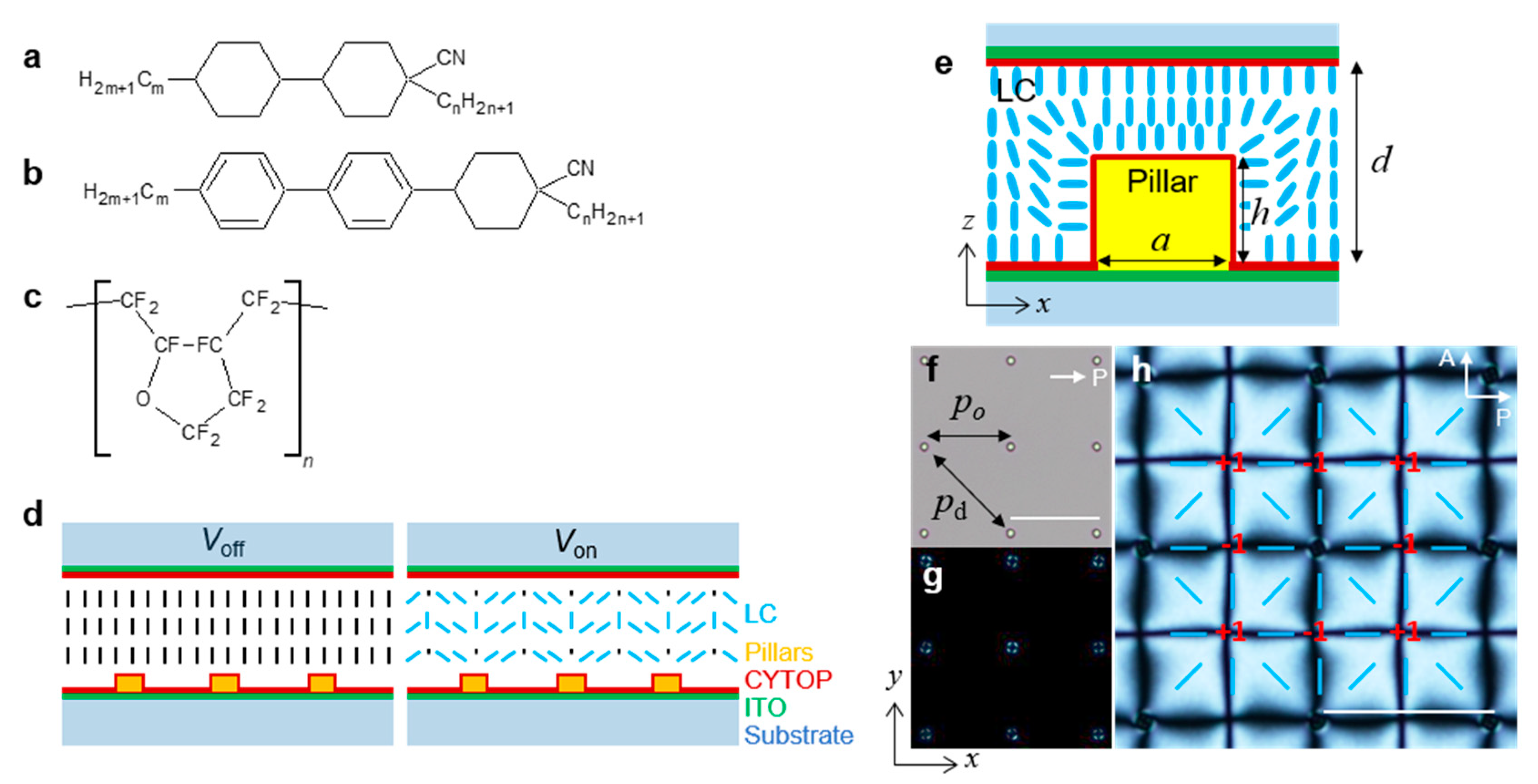
We confined LCs between one transparent indium tin oxide (ITO) electrode and a second ITO electrode patterned with UV-curable polymer (SU-8, MicroChem Corp., Westborough, MA, USA) micropillars, fabricated via photolithography. The cylindrical shape of the pillars was observed with optical microscopy by tilting them. To ensure the high conductivity of LC necessary for the formation of the defect pattern, we added a small amount (<1 wt%) of tetra butyl ammonium benzoate (TBABE) into the LC. We spin-coated a fluorinated polymer, CYTOP (Figure 1c), which gives the homeotropic alignment to both the pillars and the ITO, following the procedure outlined in [22,24]. A CCN-mn (Δn = 0.03) mixture consisted of CCN-47 and CCN-55 (Nematel GmbH & Co. KG, Mainz, Germany), nematic at room temperature (Figure 1a). The LCs were reoriented in a 2D array of umbilical defects by applying a sinusoidal waveform via a function generator (DS345, SRS Inc., Sunnyvale, CA, USA). The properties of the defect array were first characterized by Sasaki et al. [22] and during our previous work [25]. The characteristic distance between the defects is a function of the electric field properties, the material elastic and dielectric properties and the geometry of the system. The first important control on this characteristic distance is given by the cell thickness: the smaller the cell gap, the shorter is the distance [22]. Given a certain cell thickness, adjusting the voltage and frequency of the applied signal changes the spacing between two extremes, lmin and lmax. The defect array state only exists within a limited range of applied voltage and frequency, and these two parameters are not independent. At a certain given voltage, increasing the frequency causes the Freedericksz transition. Similarly, increasing voltage at a fixed frequency leads to the Freedericksz transition, and consequently the formation of the array. Above the threshold, fixing one of the two parameters and adjusting the other allows only for tunability within a few microns. A larger effect is achieved if voltage and frequency are tuned simultaneously. Frequency, voltage, and defect spacing are in this relation: l ∝ Varray/farray, where Varray and farray are above the threshold, as detailed in [22,25].
We note that it is possible to adjust the birefringence of the LC mixture by adding NCB-53 (Δn = 0.149) (Figure 1b) to the CCN-mn mixture to optimize the optical property [24]. Here, for the diffraction experiments we used a mixture with 25% CCN-47, 25% CCN-55, and 50% NCB-53. The average refractive index of the mixture is 1.523, which can be compared to the refractive index of the polymer SU-8 1.596. The birefringence of the mixture is Δn = 0.09. We used a He-Ne laser (633 nm) as a probe for electro-optic measurements. The incident laser beam travels through the sample cell and is detected by an optical power and energy meter (PM100D, Thorlabs Inc., Newton, NJ, USA).
3. Results and Discussion
A LC mixture (Figure 1a,b) was incorporated into a cell with patterned micropillars coated with CYTOP (Figure 1c) for homeotropic anchoring, as shown in Figure 1d. There is a slight distortion of LCs around the pillars owing to the homeotropic alignment at the pillar wall (Figure 1e–g). This initial distortion acts as a cue to orient the LC when the defect array is created by applying an alternating field above the threshold voltage at a certain frequency. Thus, we create +1 and −1 umbilical defects alternatingly in the array, where a fraction of the umbilical defects with charge +1 is effectively replaced by the radial director field around the pillars, as observed by polarizing optical microscopy (POM) as in Figure 1h. In this work, we focus on the specific role of the micropillars on the formation and properties of the defect patterns. In Section 3.1, we explore the effect of the pillar diameter at fixed height by POM when switching. Here, we need to specify that we use the same term “switching” to describe two different events: (1) the switching between different orientations of the defect pattern, which happens when adjusting the voltage and frequency simultaneously; and (2) the switching between the voltage-on and voltage-off states of the defect array when we characterize thethe response time, an important parameter for applications. In Section 3.2, we show how the static responses (transmittance, diffraction efficiency) and the dynamic responses (response time) are influenced by both pillar diameter and height. In Section 3.3 we demonstrate how square-shaped pillars affect the defect array formation.
3.1. Effect of the Diameter in Cylindrical Pillars on the Switching Between Patterns
The switching of the defect array relies on the elastic deformation of the LC director in the presence of the pillars. There are two main rules: (i) LC director profile around the pillars has a radial symmetry as +1 defects, while −1 defects must be accommodated in between pillars; and (ii) the scale of the intrinsic defect spacing l and the pillar spacing p must satisfy the relation p ~ ml (m = even integers). We note that l is the only parameter we can actively control. The defect spacing l strongly depends on the cell thickness d. Once d is fixed, l is tunable within a certain range by changing the voltage V and frequency f of an applied waveform V = V0 cos(2πft), as detailed in the original paper by Sasaki et al. [22] and in our previous work [24,25]. In the square array of cylindrical pillars, we can consider two different separations between micropillars, either along the orthogonal direction po or along the diagonal direction pd (Figure 1f). When l changes, it may be better accommodated either by po or by pd. Depending on how well po ~ ml and pd ~ ml are satisfied, the direction of the array changes from orthogonal to diagonal. However, this would be exactly true if the pillar diameter were very small compared to l. In reality, the pillars’ finite diameter shortens the available space to accommodate defects in the array and subsequently it affects the behavior of the system.
We reduced l by changing the field frequency and voltage from 60 Hz and 11 V to 120 Hz and 6 V, as shown in Figure 2. When l becomes shorter, po ~ 2l changes to pd ~ 4l. The transition between patterns I and II occurs at f (V) ~ 80 Hz (8 V), 90 Hz (7.5 V), 100 Hz (7 V), and 120 Hz (6 V) for pillar diameters a = 2, 4, 6, 8 μm, respectively, as shown in Figure 2a–d (the height of pillars is fixed at h = 3 μm). We define p as the distance between the centers of the pillars. Thus, the actual space available for the LC in between pillars changes as a changes. For instance, varying the pillar diameter a = 2, 4, 6, 8 μm, the actual pillar spacing is 48, 46, 44, 42 μm, respectively. The shorter pd requires shorter l to satisfy pd ~ 4l, thus the transition occurs at shorter l. The last row of Figure 2 also shows how the choice of large pillars can entirely suppress the pattern switching. The pillar diameter thus provides a further “knob” of this system to control the transition point between the two array orientations.
3.2. Electro-Optic Properties Depending on the Diameter and Height of Cylindrical Pillars
The defect patterns we create work as good 2D transmission diffraction gratings thanks to the spontaneous modulation of the refractive index [24]. A He-Ne laser beam (λ ~ 633 nm) travels through the sample cells and the diffraction patterns are observed on a dark screen. The images in Figure 3a show the diffraction pattern from defect arrays formed with small (4 μm) or large (8 μm) pillars. Here, the diffraction patterns correspond to arrays shown in Figure 2b,d. As expected, the primitive unit of the lattice rotates by 45 degrees when a higher frequency and lower voltage field is applied. For the4 μm pillars, this effect is very evident in the diffraction pattern, which shows a change in both azimuthal and polar angle, following the relation pd ~ 4l. The same effect is also visible in the pattern generated with 8 μm pillars.
The frequency-dependent transmittance of the probe laser beam traveling through the sample cell at a fixed voltage shows how much light is scattered only by the pillars (with homeotropic LC alignment) and by the created defect patterns. Considering the voltage-off state, the pillars distort the homeotropic alignment of LC in the ground state (Figure 1e,g). If the height of the pillars is much shorter than the cell thickness, the light scattering from the pillars is negligible. For our choice of LC mixture, we have not detected any scattering by pillars shorter than 2 μm. However, bigger pillars scatter light more, which gives rise to low transmittance of the probe laser light at the voltage-off state. The green dotted lines in Figure 3b indicate the difference of optical intensity. This can also be seen in the voltage-off state in Figure 3a. For diameters up to 4 μm, the scattering from the pillar array is almost negligible, but it becomes significant for 8 μm pillars. We observed that the threshold frequency needed to induce the pattern decreases as the pillar diameter a increases (Figure 3b). A larger a implies a larger surface area of the pillars, hence a bigger total surface energy and a spontaneous alignment of the LC on the surface of the pillars. The distorted LC configuration is closer to radial around the +1 defects, also without an applied field. Thus, the required energy to reorient the LC director upon applying the electric field becomes smaller.
We also measured the rising and falling response times switching between the voltage-on and voltage-off states with respect to various h and a at a fixed cell thickness d = 9.3 μm (Figure 3c–e and Table 1). Both the lateral surface area and the volume of the LC on top of the pillars contribute to determining the response time. As the lateral surface area of the pillars increases, more LCs are already aligned on the xy-plane and therefore the response time is faster. However, if the pillars become too large, other effects come into play, such as those visible in Figure 3f. The image shows pillars with a = 4, 6, 8 μm when the same electric field is applied (the field is stronger than that applied in Figure 2). When a = 4 μm, it is possible to see that the +1 defect is not exactly localized at the pillar, and the pillar itself has defects. When a = 8 μm, we observe a large twist around the pillar. This occurs because of the high free energy cost of the bend/splay elastic deformations along the z-axis caused by the large pillar diameter. The bend is partly converted into twist deformation, which has a smaller energy cost.
3.3. Effect of Square-Shaped Pillars on the Defect Array Formation
In the previous results, one of the key features was that the pillars acted as small perturbations to some nodes of the array. The switch between the orthogonal and the diagonal direction was seamless because the LCs were free to explore all the surrounding space. In fact, the switching between the two configurations was not previously observed, when the arrays were created within square confinement imposed by patterned electrodes [22,25]. We wanted to investigate what happens if certain parts of the arrays are confined only by nodes and others are confined by edges. For this, we used micropillars with a square cross-section. The square-shaped pillars were created so that the lateral size of the pillars w equals the spacing p between them along the square lattice. We explored the range w = p = 5–40 μm (Figure 4). The first difference emerges before the field is applied.
We analyzed the LC director configuration under crossed polarizers and with an inserted full-wave plate. In the case of cylindrical pillars, we mostly observed 4-brushes (e.g., in Figure 1h), as expected for the radial alignment around the pillars. From square-shaped pillars, we often observed 6-brushes, as the schematic shown in Figure 4(d2). The likely reason is the sharpness of the pillars’ edges, which causes the formation and the pinning of defect lines, as shown also by Beller et al. in sharp colloids [26]. This LC distortion in the array with the shorter w and p (for instance, when w = p = 5 μm in Figure 4(a2)) propagates to the neighboring regions around the pillars. The slight light leakage in the POM image under crossed polarizers shows that the LC deformation between pillars influences the director field of the neighboring pillars.
Upon applying electric fields with frequencies ranging f = 150–1000 Hz, and voltages ranging V = 53.3–8.4 V, we observed no regular defect array when w = p = 5 μm (Figure 5a), but defect arrays are visible in the arrays of square-shaped pillars with w = p = 10 and 20 μm (Figure 5b,c). In the pillar array with the smallest spacing, defect lines are pinned at the pillars and the umbilical defect pattern is suppressed entirely. In the array with w = p = 10, 20 μm, the pattern of umbilical defects appears, but it does not switch to another orientation over the range of frequency and voltage applied. In this configuration, we observe that the areas in between four pillars have one defect in the center and that the areas in between two pillar walls also have one defect each.
In the case of w = p = 40 μm, the defect array is able to transition between field-induced stable states. At f = 150 Hz, V = 53.3 V (Figure 6a), the defect pattern is arranged in a square array, with one defect at the intersection, similar to the array with w = p = 10, 20 μm (Figure 5b,c). The configuration obtained at a higher frequency, however, is hybrid. The areas between two pillars maintain the previous orthogonal configuration with only one defect, albeit slightly distorted as can be seen, for example, comparing that region in Figure 6(a3,c3). The areas between four pillars, instead, are occupied by defects arranged along a diagonal lattice. At intermediate frequencies and voltages, it is possible to see a clear transition region between the two states, characterized by a progressive switch from orthogonal to diagonal lattice alignment in the region between four pillars (Figure 6b). A complete switch to a square lattice with diagonal alignment would be possible by changing the pillar array lattice to a hexagonal lattice, as demonstrated by Kim et al. [27].
The formation of defect arrays is highly dependent on the ratio of the cell thickness d to the pillar spacing p. When p > 2d, the relation p ~ ml can be satisfied in certain ranges of voltages and frequencies. However, when p is similar to or smaller than d, no patterns are created as in the case of w = p = 5 μm in Figure 7a. With similar pillar arrays, but greater cell thicknesses, the defects do not appear. Instead, upon applying the electric field, we observed a uniform homogeneous LC alignment as d = 11 μm in Figure 7a,b, which is approximately twice as large as the cell thickness in Figure 6. In this region, although the defect array formation is suppressed, we can still see modulation of the refractive index/birefringence, with a smaller amplitude of the modulation. As expected, the LCs are uniformly aligned along the diagonal direction with respect to the pillar arrays, as also reported in other LC systems [28].
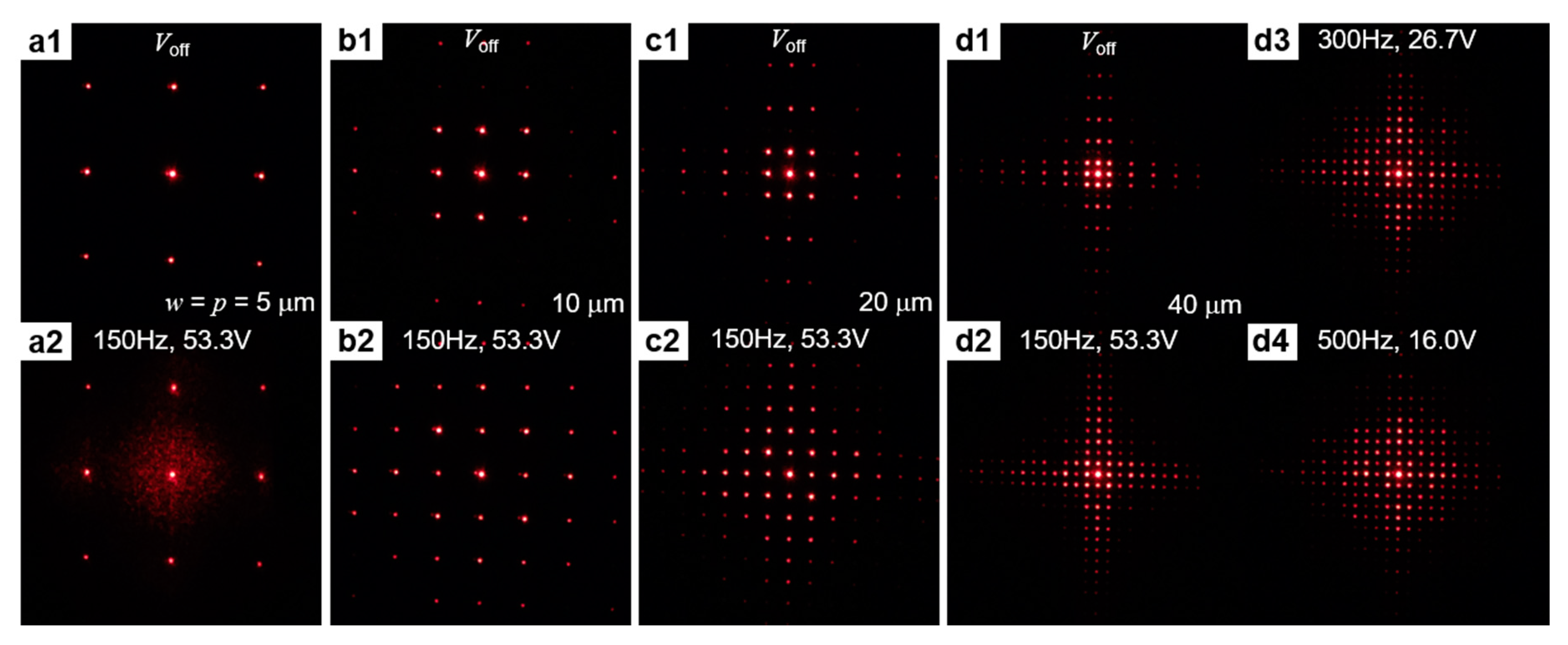
Finally, we observed the diffraction patterns created by the samples with square-shaped pillars (Figure 8). In the voltage-off state, the diffraction patterns are created only by pillars. The diffraction angle in these patterns becomes smaller as the width w and spacing p of the pillar array are increased (Figure 8(a1–d1)). The diffraction patterns in Figure 8(a1–d1) correspond to the POM images of the pillar arrays in Figure 4a–d. Similarly, the diffraction patterns in Figure 8(a2–c2,d2–d4) correspond to Figure 5a–c and Figure 6(a–c). In the case w = p = 5 μm, the pattern does not change upon applying voltage, but some cloud-like scattering occurs due to the random LC director distribution and the presence of defect lines. The situation is different for larger pillars with w = 10, 20 μm, and the differences are more striking with w = 40 μm. One single defect appears in the areas adjacent to four pillars with w = 10, 20 μm (Figure 5b,c) and the corresponding diffraction spots do not change by tuning the electric field (Figure 8(b2,c2)). When w = p = 40 μm, the field at f = 300 Hz, V = 26.70 V (Figure 6b and Figure 8(d3)) drives the appearance of more diffraction spots in the diagonal direction due to the three defects in the areas adjacent to four pillars. As the defects are more closely spaced than the pillars, the diffraction intensity increases at large angles and decreases at small angles. Upon applying the field at f = 500 Hz, V = 16.0 V, five defects are arranged in the diagonal direction (Figure 6c), on a lattice with a shorter primitive unit, which corresponds to an even larger diffraction angle (Figure 8(d4)).
4. Conclusions
We investigated the effect of the size of pillars in the formation and optical properties of the defect arrays. The pillars are necessary for the creation of regular, large-scale, and switchable domains. We found that pillars smaller than 4 μm in diameter, do not greatly alter the optical properties of the diffraction grating formed with the defect array, while larger pillars do. Large pillars, however, lower the threshold voltage for the formation of the array. The voltage/frequency required to switch between two orientations of the defect array is also affected by the pillars’ diameter, so that larger pillars create a larger metastable, disordered region between the two stable states, or suppress the switching entirely. The response time is affected by the total surface area of the micropillars.
We explored the effect of pillars with square cross-section that divide the array in connected pixels. Small squares completely suppress the array formation and instead promote, depending on the ratio between the height of the pillars and that of the cell, either a highly defected state or a uniform alignment of the liquid crystals when the electric field is applied. Larger features show the same switchable two-state behavior in the regions between four adjacent squares as the one observed with the individual small pillars, while different configurations are not admitted in the more confined regions between two square walls. Using square-shaped pillars, it is possible to create systems where only certain regions respond to the external field, while maintaining a regular background array.
The control of defect arrays with a combination of topographic features and external fields is a powerful tool that can be used for switchable LC-based optical components. This work shows that the geometry of the features is key in determining the behavior of the systems and allows for a fine tuning of parameters such as threshold voltage, response time, transition field between different states, and fraction of switchable regions of the array.
Author Contributions
Conceptualization, M.K. and F.S; Methodology, M.K. and F.S.; Investigation, M.K.; writing, M.K. and F.S.; and funding acquisition, F.S. All authors have read and agreed to the published version of the manuscript.
Funding
This research was funded by Johns Hopkins University and by ACS PRF 59931-DNI10.
Acknowledgments
We would like to thank Alvin Modin for the helpful suggestions.
Conflicts of Interest
The authors declare no conflict of interest.
References
- Blanc, C.; Coursault, D.; Lacaze, E. Ordering nano- and microparticles assemblies with liquid crystals. Liq. Cryst. Rev. 2013, 1, 83–109. [Google Scholar] [CrossRef]
- Muševič, I. Integrated and topological liquid crystal photonics. Liq. Cryst. 2014, 41, 418–429. [Google Scholar] [CrossRef]
- Bukusoglu, E.; Bedolla Pantoja, M.; Mushenheim, P.C.; Wang, X.; Abbott, N.L. Design of responsive and active (soft) materials using liquid crystals. Annu. Rev. Chem. Biomol. Eng. 2016, 7, 163–196. [Google Scholar] [CrossRef] [PubMed]
- de Gennes, P.-G.; Prost, J. The Physics of Liquid Crystals, 2nd ed.; Oxford University Press Press: Oxford, UK, 1993; ISBN 0198512856. [Google Scholar]
- Kléman, M. Defects in liquid crystals. Rep. Prog. Phys. 1989, 52, 555–654. [Google Scholar] [CrossRef]
- Poulin, P.; Stark, H.; Lubensky, T.C.; Weitz, D.A. Novel colloidal interactions in anisotropic fluids. Science 1997, 275, 1770–1773. [Google Scholar] [CrossRef] [Green Version]
- Nych, A.; Ognysta, U.; Škarabot, M.; Ravnik, M.; Žumer, S.; Muševič, I. Assembly and control of 3D nematic dipolar colloidal crystals. Nat. Commun. 2013, 4, 1489. [Google Scholar] [CrossRef]
- Luo, Y.; Beller, D.A.; Boniello, G.; Serra, F.; Stebe, K.J. Tunable colloid trajectories in nematic liquid crystals near wavy walls. Nat. Commun. 2018, 9, 1–11. [Google Scholar] [CrossRef] [Green Version]
- Bowick, M.J.; Chandar, L.; Schiff, E.A.; Srivastava, A.M. The cosmological Kibble mechanism in the laboratory: String formation in liquid crystals. Science 1994, 263, 943–945. [Google Scholar] [CrossRef] [Green Version]
- Tkalec, U.; Ravnik, M.; Čopar, S.; Žumer, S.; Muševič, I. Reconfigurable knots and links in chiral nematic colloids. Science 2011, 333, 62–65. [Google Scholar] [CrossRef] [Green Version]
- Senyuk, B.; Liu, Q.; He, S.; Kamien, R.D.; Kusner, R.B.; Lubensky, T.C.; Smalyukh, I.I. Topological colloids. Nature 2013, 493, 200–205. [Google Scholar] [CrossRef] [Green Version]
- Brasselet, E. Tunable optical vortex arrays from a single nematic topological defect. Phys. Rev. Lett. 2012, 108, 087801. [Google Scholar] [CrossRef] [PubMed]
- Serra, F.; Eaton, S.M.; Cerbino, R.; Buscaglia, M.; Cerullo, G.; Osellame, R.; Bellini, T. Nematic liquid crystals embedded in cubic microlattices: Memory effects and bistable pixels. Adv. Funct. Mater. 2013, 23, 3990–3994. [Google Scholar] [CrossRef]
- Lopez-Leon, T.; Bates, M.A.; Fernandez-Nieves, A. Defect coalescence in spherical nematic shells. Phys. Rev. E-Stat. Nonlinear Soft Matter Phys. 2012, 86, 030702. [Google Scholar] [CrossRef] [PubMed]
- Lavrentovich, O.D. Topological defects in dispersed liquid crystals, or words and worlds around liquid crystal drops. Liq. Cryst. 1998, 24, 117–125. [Google Scholar] [CrossRef]
- Kamien, R.D. The geometry of soft materials: A primer. Rev. Mod. Phys. 2002, 74, 953–971. [Google Scholar] [CrossRef] [Green Version]
- Stein, D.L. Topological theorem and its applications to condensed matter systems. Phys. Rev. A 1979, 19, 1708–1711. [Google Scholar] [CrossRef]
- Keber, F.C.; Loiseau, E.; Sanchez, T.; DeCamp, S.J.; Giomi, L.; Bowick, M.J.; Marchetti, M.C.; Dogic, Z.; Bausch, A.R. Topology and dynamics of active nematic vesicles. Science 2014, 345, 1135–1139. [Google Scholar] [CrossRef] [Green Version]
- Serra, F. Curvature and defects in nematic liquid crystals. Liq. Cryst. 2016, 43, 1920–1936. [Google Scholar] [CrossRef]
- Peng, C.; Turiv, T.; Guo, Y.; Wei, Q.H.; Lavrentovich, O.D. Command of active matter by topological defects and patterns. Science 2016, 354, 882–885. [Google Scholar] [CrossRef] [Green Version]
- Murray, B.S.; Pelcovits, R.A.; Rosenblatt, C. Creating arbitrary arrays of two-dimensional topological defects. Phys. Rev. E-Stat. Nonlinear Soft Matter Phys. 2014, 90, 052501. [Google Scholar] [CrossRef] [Green Version]
- Sasaki, Y.; Jampani, V.S.R.; Tanaka, C.; Sakurai, N.; Sakane, S.; Le, K.V.; Araoka, F.; Orihara, H. Large-scale self-organization of reconfigurable topological defect networks in nematic liquid crystals. Nat. Commun. 2016, 7, 13238. [Google Scholar] [CrossRef] [PubMed]
- Migara, L.K.; Song, J.-K. Standing wave-mediated molecular reorientation and spontaneous formation of tunable, concentric defect arrays in liquid crystal cells. NPG Asia Mater. 2018, 10, e459. [Google Scholar] [CrossRef] [Green Version]
- Kim, M.S.; Serra, F. Tunable dynamic topological defect pattern formation in nematic liquid crystals. Adv. Opt. Mater. 2020, 8, 1900991. [Google Scholar] [CrossRef]
- Kim, M.S.; Serra, F. Tunable large-scale regular array of topological defects in nematic liquid crystals. RSC Adv. 2018, 8, 35640–35645. [Google Scholar] [CrossRef] [Green Version]
- Beller, D.A.; Gharbi, M.A.; Liu, I.B. Shape-controlled orientation and assembly of colloids with sharp edges in nematic liquid crystals. Soft Matter 2015, 11, 1078–1086. [Google Scholar] [CrossRef] [Green Version]
- Kim, D.S.; Čopar, S.; Tkalec, U.; Yoon, D.K. Mosaics of topological defects in micropatterned liquid crystal textures. Sci. Adv. 2018, 4, eaau8064. [Google Scholar] [CrossRef] [Green Version]
- Lohr, M.A.; Cavallaro, M., Jr.; Beller, D.A.; Stebe, K.J.; Kamien, R.D.; Collings, P.J.; Yodh, A.G. Elasticity-dependent self-assembly of micro-templated chromonic liquid crystal films. Soft Matter 2014, 10, 3477–3484. [Google Scholar] [CrossRef] [Green Version]
Figure 1.
Molecular structures of materials and schematics of the LC/Pillar system: (a) CCN-mn; (b) NCB-mn; and (c) CYTOP. (d) Schematic of the LC director field at voltage off/on. (e) Schematic of LC director field and substrate structure. (f) Square array of cylindrical pillars. (g) Homeotropic LC configuration: slightly distorted LCs around pillars (brightness and contrast are adjusted for visibility). (h) LC configuration with +1 and -1 umbilical defects. P, polarizer; A, analyzer. Scale bars are 40 μm.

Figure 2.
Defect array formation observed by polarizing optical microscopy with a full-wave plate inserted at 45 degrees between the crossed polarizers (used to distinguish +1 from −1 defects), when varying the pillar diameter a: (a) a = 2 μm; (b) a = 4 μm; (c) a = 6 μm; and (d) a = 8 μm. Pillar height is h = 3 μm, cell thickness is d = 5.4 μm, and po = 50 μm. P, polarizer; A, analyzer; λ, full-wave plate. The red dots and white-dotted line indicate a broken-square domain surrounded by six defects. Scale bar is 50 μm.

Figure 3.
The electro-optical measurement when varying the diameter a and height h of pillars. (a) Diffraction patterns with cylindrical pillars. The height of pillars is h = 2 μm, the cell thickness is d = 3.8 μm, and the LC mixture consists of NCB-53/CCN-47/CCN-55 (50/25/25). (b) The frequency-dependent transmittance curves at h = 3 μm. The green dotted lines indicated by the green arrows show the difference of optical intensity. (c–e) The rising time τon and falling time τoff. The values of the response time and applied frequency are shown in Table 1. Cell thickness is d = 9.3 μm and V = 10 V in (b–h). (f) Chirality shown in POM images of LC with a = 4, 6, 8 μm with the same applied field.

Figure 4.
The array of square-shaped pillars with pillar width w and pillar spacing p observed by polarizing optical microscopy (POM): (a) w = p = 5 μm; (b) w = p = 10 μm; (c) w = p = 20 μm; and (d) w = p = 40 μm. POM images: (a1–d1) under crossed polarizers with brightness adjusted for visibility; and (a2–d2) under crossed polarizers with a full-wave plate. Pillar height is h = 2 μm and cell thickness is 5.6 μm. P, polarizer; A, analyzer; λ, full-wave plate. The schematic in (d2) represents LC director near a pillar.

Figure 5.
Defect array formation in square-shaped pillars with width w and spacing p of pillars observed by polarizing optical microscopy: (a) w = p = 5 μm; (b) w = p = 10 μm; and (c) w = p = 20 μm. (a1–c1) Under crossed polarizers in the orthogonal direction; (a2–c2) with a full-wave plate; and (a3–c3) in the diagonal direction. Pillar height is h = 2 μm and cell thickness is d = 5.6 μm. P, polarizer; A, analyzer; λ, full-wave plate. The red dots are umbilical defects; the blue square represents pillars.

Figure 6.
Defect array formation and transition in square-shaped pillars of w = p = 40 μm observed by polarizing optical microscopy: (a) f = 150 Hz, V = 53.3 V; (b) f = 300 Hz, V = 26.70 V; and (c) f = 500 Hz, V = 16.0 V. (a1–c1) Under crossed polarizers in the orthogonal direction; (a2–c2) with a full-wave plate; and (a3–c3) at 45 degrees, as indicated in the inset. Pillar height is h = 2 μm and cell thickness is d = 5.6 μm. P, polarizer; A, analyzer; λ, full-wave plate. The red dots are umbilical defects; the blue square is the central pillar; and the yellow lines indicate the lattice at 0 or 45 degrees and are a guide for the eye.

Figure 7.
Effect of cell thickness on the defect formation with respect to pillar width w and pillar spacing p: (a) w = p = 5 μm; and (b) w = p = 10 μm. Cell thickness d = 11 μm, pillar height h = 2 μm. P, polarizer; A, analyzer; λ, full-wave plate.
Figure 7.
Effect of cell thickness on the defect formation with respect to pillar width w and pillar spacing p: (a) w = p = 5 μm; and (b) w = p = 10 μm. Cell thickness d = 11 μm, pillar height h = 2 μm. P, polarizer; A, analyzer; λ, full-wave plate.

Figure 8.
Diffraction patterns with square-shaped pillars: (a) w = p = 5; (b) w = p = 10; (c) w = p = 20; and (d) w = p = 40 μm. (a1–d1) Voltage-off state; (a2–d2) f = 150 Hz, V = 53.3 V; (d3) f = 300 Hz, V = 26.70 V; and (d4) f = 500 Hz, V = 16.0 V. Cell thickness is d = 5.6 μm and pillar height is h = 2 μm.


Table 1.
The measured response times in Figure 3a–g.
Table 1.
The measured response times in Figure 3a–g.
| a1 (μm) | 4 | 6 | 8 | ||||||
| h2 (μm) | 2 | 3 | 5 | 2 | 3 | 5 | 2 | 3 | 5 |
| f3 (Hz) | 220 | 240 | 240 | 210 | 220 | 220 | 200 | 200 | 180 |
| V4 (V) | 10 | 10 | 10 | 10 | 10 | 10 | 10 | 10 | 10 |
| τon5 (s) | 0.49 | 0.34 | 0.26 | 0.44 | 0.27 | 0.28 | 0.28 | 0.28 | 0.37 |
| τoff6 (s) | 0.24 | 0.19 | 0.14 | 0.17 | 0.16 | 0.16 | 0.19 | 0.20 | 0.19 |
| τon error | 0.03 | 0.03 | 0.03 | 0.04 | 0.04 | 0.04 | 0.03 | 0.03 | 0.04 |
| τoff error | 0.03 | 0.03 | 0.03 | 0.04 | 0.03 | 0.03 | 0.03 | 0.03 | 0.03 |
1 Diameter of pillars; 2 height of pillars; 3 frequency; 4 voltage; 5 rising time; 6 falling time.
© 2020 by the authors. Licensee MDPI, Basel, Switzerland. This article is an open access article distributed under the terms and conditions of the Creative Commons Attribution (CC BY) license (http://creativecommons.org/licenses/by/4.0/).
Share and Cite
MDPI and ACS Style
Kim, M.; Serra, F. Topological Defect Arrays in Nematic Liquid Crystals Assisted by Polymeric Pillar Arrays: Effect of the Geometry of Pillars. Crystals 2020, 10, 314. https://0-doi-org.brum.beds.ac.uk/10.3390/cryst10040314
AMA Style
Kim M, Serra F. Topological Defect Arrays in Nematic Liquid Crystals Assisted by Polymeric Pillar Arrays: Effect of the Geometry of Pillars. Crystals. 2020; 10(4):314. https://0-doi-org.brum.beds.ac.uk/10.3390/cryst10040314
Chicago/Turabian StyleKim, MinSu, and Francesca Serra. 2020. "Topological Defect Arrays in Nematic Liquid Crystals Assisted by Polymeric Pillar Arrays: Effect of the Geometry of Pillars" Crystals 10, no. 4: 314. https://0-doi-org.brum.beds.ac.uk/10.3390/cryst10040314
Note that from the first issue of 2016, this journal uses article numbers instead of page numbers. See further details here.