Carbon Nanotube Detectors and Spectrometers for the Terahertz Range


1
Department of Electrical, Computer, and Systems Engineering, Rensselaer Polytechnic Institute, Troy, NY 12180, USA
2
Department of Electronic Systems, Norwegian University of Science and Technology, O.S. Bragstads plass 2a, 7034 Trondheim, Norway
3
Electronics of the Future, Inc., Vienna, VA 22181, USA
*
Author to whom correspondence should be addressed.
Crystals 2020, 10(7), 601; https://0-doi-org.brum.beds.ac.uk/10.3390/cryst10070601
Submission received: 28 May 2020
/
Revised: 7 July 2020
/
Accepted: 8 July 2020
/
Published: 10 July 2020
(This article belongs to the Special Issue Plasmonic Nanostructures)
Abstract
:We present the compact unified charge control model (UCCM) for carbon nanotube field-effect transistors (CNTFETs) to enable the accurate simulation of the DC characteristics and plasmonic terahertz (THz) response in the CNTFETs. Accounting for the ambipolar nature of the carrier transport (n-type and p-type conductivity at positive and negative gate biases, respectively), we use n-type and p-type CNTFET non-linear equivalent circuits connected in parallel, representing the ambipolar conduction in the CNTFETs. This allows us to present a realistic non-linear model that is valid across the entire voltage range and is therefore suitable for the CNTFET design. The important feature of the model is that explicit equations for gate bias, current, mobility, and capacitance with smoothing parameters accurately describe the device operation near the transition from above- to below-threshold regimes, with scalability in device geometry. The DC performance in the proposed compact CNTFET model is validated by the comparison between the SPICE simulation and the experimental DC characteristics. The simulated THz response resulted from the validated CNTFET model is found to be in good agreement with the analytically calculated response and also reveals the bias and power dependent sub-THz response and relatively wide dynamic range for detection that could be suitable for THz detectors. The operation of CNTFET spectrometers in the THz frequency range is further demonstrated using the present model. The simulation exhibits that the CNT-based spectrometers can cover a broad THz frequency band from 0.1 to 3.08 THz. The model that has been incorporated into the circuit simulators enables the accurate assessment of DC performance and THz operation. Therefore, it can be used for the design and performance estimation of the CNTFETs and their integrated circuits operating in the THz regime.
1. Introduction
Recent breakthrough in fabricating a carbon nanotube (CNT) microprocessor highlights the potential for CNT applications [1]. CNTs have unique electrical properties, particularly quasi-ballistic transport and high carrier mobility, making them potential candidates for high-frequency applications, including applications in the terahertz range of frequencies. A compact design CNT model implemented in a standard computer-aided design (CAD) environment, such as CADENCE or ADS [2], is a prerequisite for the development of the CNT-based THz detectors, mixers, frequency multipliers, and sources operating in a circuit environment. Analytical models to represent a ballistic and an ambipolar carbon nanotube field-effect transistor (CNTFET) were developed [3,4,5], and circuit compatible models for CNTFETs based on the fundamental properties of CNTs were reported [6,7,8,9,10]. In this paper, we propose a compact unified charge control model (UCCM) for CNT-based FETs that are valid for THz frequencies. This model offers accurate descriptions of the ambipolar DC characteristics of the CNTFET and the device operation in the THz regime under both positive and negative gate biases.
2. Unified Charge Control Model for Ambipolar CNTFETs
2.1. Model Description
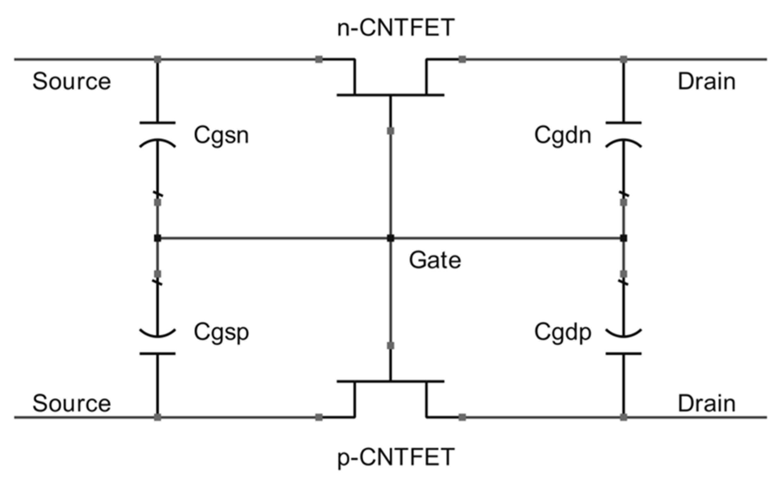
Ambipolar conduction has been demonstrated as a transfer characteristic of CNTFETs and is explained by the dominance of electrons or holes in the channel due to the thermionic emission and tunneling mechanisms at the source-sided and drain-sided Schottky barriers under different gate and drain biases [3,5,11]. To model this behavior, we introduce an n-type CNTFET and a p-type CNTFET (n-CNTFET and p-CNTFET) connected in parallel to represent the intrinsic elements for channel conduction. When the applied gate bias changes from negative to positive voltage or vice versa, the CNTFET channel will change from one type to the other. Figure 1 depicts the equivalent circuit representing the proposed CNTFET SPICE model without including extrinsic elements. The intrinsic gate-to-source capacitance () and the gate-to-drain capacitance ( of the CNTFET are also implemented in the model to account for the intrinsic charge distribution.
The equations for the CNTFET model are based on the UCCM, which has been used for MOSFET, MESFET, and HFET modeling [12,13,14,15]. This universality of UCCM is due to the fact that the model treats an FET as a charge controlling device and a potential barrier device in the above- and below-threshold regimes, respectively, using the unified and continuous equations which are suitable for circuit simulations and are also scalable with geometry and bias [14,15].
The current–voltage characteristics of the intrinsic CNTFET are expressed by the universal interpolation equation as follows:
where is the parameter for channel length modulation; is the extrinsic drain-to-source bias; is the adjustable exponent determining the saturation transition of the output conductance; is the effective, extrinsic saturation voltage, ; is the saturation current; is the extrinsic channel conductance, ; and are the source and drain series resistance, respectively; and is the intrinsic channel conductance.
Equation (1) describes a continuous and smooth transition between the linear and the saturation region. The drain current in the linear region is given by . The output characteristics in the saturation region can be described by the factor and hence the output conductance in well-above saturation is dependent on [14,15].
At large drain-to-source voltages, the drain current saturates when the charge carrier velocity becomes equal to the effective saturation velocity, To express the drain saturation current , the basic saturation current equation used in Refs. [14,15] is adopted as follows:
where is the characteristic voltage of velocity saturation, is the channel mobility, is the channel length, and is the effective gate voltage swing accounting for both above and below threshold values:
where is the sub-threshold ideality factor, is the parameter controlling the transition width between above and below threshold, is the gate voltage swing, and is the thermal voltage.
The intrinsic channel conductance can be written as , where is the elementary charge and is the empirical expression of the charge carrier density accounting for the transition between the linear and saturation regime sin the CNTFET, which is given by
where is the maximum charge carrier density, is the transition parameter determining the steepness of the carrier density saturation, and is the unified charge carrier density in the channel describing a continuous transition between the above- and below-threshold regimes [14,15],
where is the gate-to-source voltage swing and is the threshold voltage.
The factor indicates the gate-to-channel capacitance per unit length comprised of the series-connected gate dielectric capacitance and CNT quantum capacitance.
Here, is the quantum capacitance expressed as , where is the adjustable quantum capacitance factor. is the gate insulator capacitance adopted from the capacitance equation between an one-dimensional wire and a plane substrate, which is given as follows [16]:
where is the gate oxide thickness, is the diameter of CNT, is the vacuum permittivity, and is the dielectric permittivity,
The channel mobility equation is developed for describing the mobility behavior in the CNTFET experimentally demonstrated in [17]
where is the above threshold mobility, is the mobility degradation parameter, is the mobility degradation exponent, is the adjustable mobility parameter, and is the adjustable mobility exponent.
To evaluate the gate-to-source capacitance ) and the gate-to-drain capacitance (), the unified equations based on the Meyer’s model [18] are implemented in the present CNTFET model.
where is the differential gate-to-channel capacitance, and is the effective, extrinsic drain-to-source bias.
2.2. Model Validation
We compared the simulated results with experimental data previously reported in [19] to validate the present CNTFET compact model. The CNTFET used in [19] is composed of a 50-nm-long single-walled nanotube (SWNT), an 8-nm-thick HfO2 gate dielectric, a top aluminum gate electrode, and palladium (Pd) source and drain contacts. The measured current–voltage characteristics show quasi-ballistic transport because of the Schottky barrier lowering at the Pd contact to p-channel SWNT, small diameter of the CNT, and thin and high- gate dielectric [19,20]. For device modeling, a series resistance (1700 ) [19] and a quantum capacitance () [21] were included.
To simulate CNTFET performance using the SPICE simulator, the model parameters for a p-CNTFET and a nominal n-CNTFET must be determined on the basis of the experimental data. We used the standard parameter extraction method [14] to approximate the parameters and in Equation (1) and the threshold voltage. In the deep saturation regime, the output conductance can be expressed as , and it is defined as the slope of the measured output characteristics at large drain bias. Likewise, the output conductance in the linear regime can be defined as a slope at small drain voltages. These two linear pieces yield an intersection point that corresponds to the saturation current, and therefore, can be estimated from the ratio of to . At the saturation voltage, the drain current can be reduced to so that parameter can be determined with the estimated . The threshold voltage can be estimated by defining the voltage point where the current begins to flow in the transfer characteristics. We finally adjusted those estimated values and determined other parameters included only in the CNTFET model via numerical optimization using the interpolation strategy to obtain the best fit of referenced data.
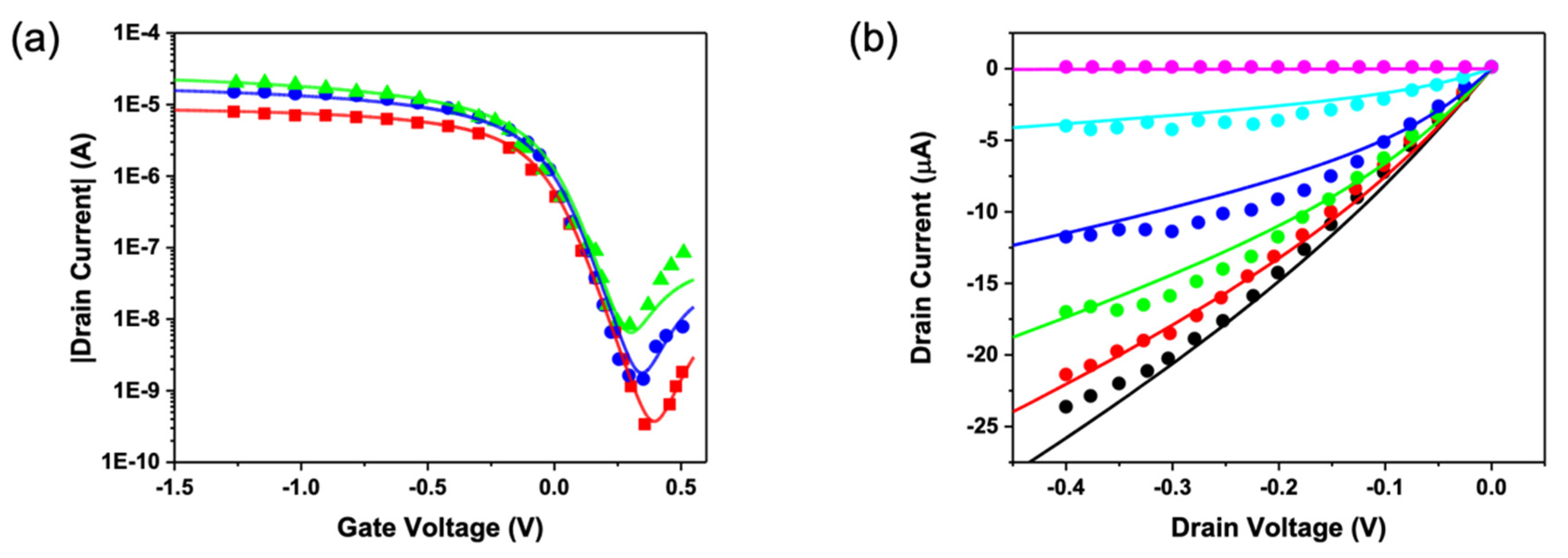
The compact CNTFET model was implemented in Verilog-A, and current–voltage characteristics were estimated through ADS simulation with the determined parameters. As shown in Figure 2, the good agreement between the simulated results and experimental data confirms that the model is valid for simulating the electrical characteristics of the CNTFETs. The channel carrier mobility for p-CNTFET and n-CNTFET was theoretically estimated based on Equation (8) and Equation (9). The n-CNTFET exhibits electron mobility that is two orders of magnitude lower than the hole mobility of the p-CNTFET due to the suppressed electron conduction, as identified in Figure 2a. The differential gate-to-channel capacitance, , which represents the variation in the charge carrier density with respect to the gate voltage, was also estimated. The maximum value of of p- and n-CNTFET was achieved in the above threshold regime corresponding to the negative and positive gate bias region, respectively. This reveals that the present CNTFET model can properly describe dominant carrier type in drain currents, and consequently, the parallel-connected CNTFETs can describe the ambipolar carrier transport characteristics.
3. THz Response in CNTFETs
The CNTFET model with the parameters determined above was used in the THz simulation in order to investigate the THz response dependence of the CNTFET on the gate voltage and the THz amplitude. Considering the ballistic characteristics of the CNTFET, the motion of charge carriers in the CNT channel can be modeled by the equations of the hydrodynamic model [22,23] as follows:
where is the charge carrier velocity, is the charge carrier concentration, is the elementary charge, is the charge carrier mass, is the gate-to-channel voltage, and is the momentum relaxation time of the carriers in the channel.
An incident THz radiation excites plasma oscillations in the channel region, and the nonlinearity of such plasma waves results in a finite DC component of source-to-drain voltage response. If an AC voltage with a frequency () is induced by the incident THz beam between the gate and the source and the amplitude of the AC voltage ( is sufficiently small, the drain voltage response ) with the open-drain boundary condition is given as follows [22,23,24]:
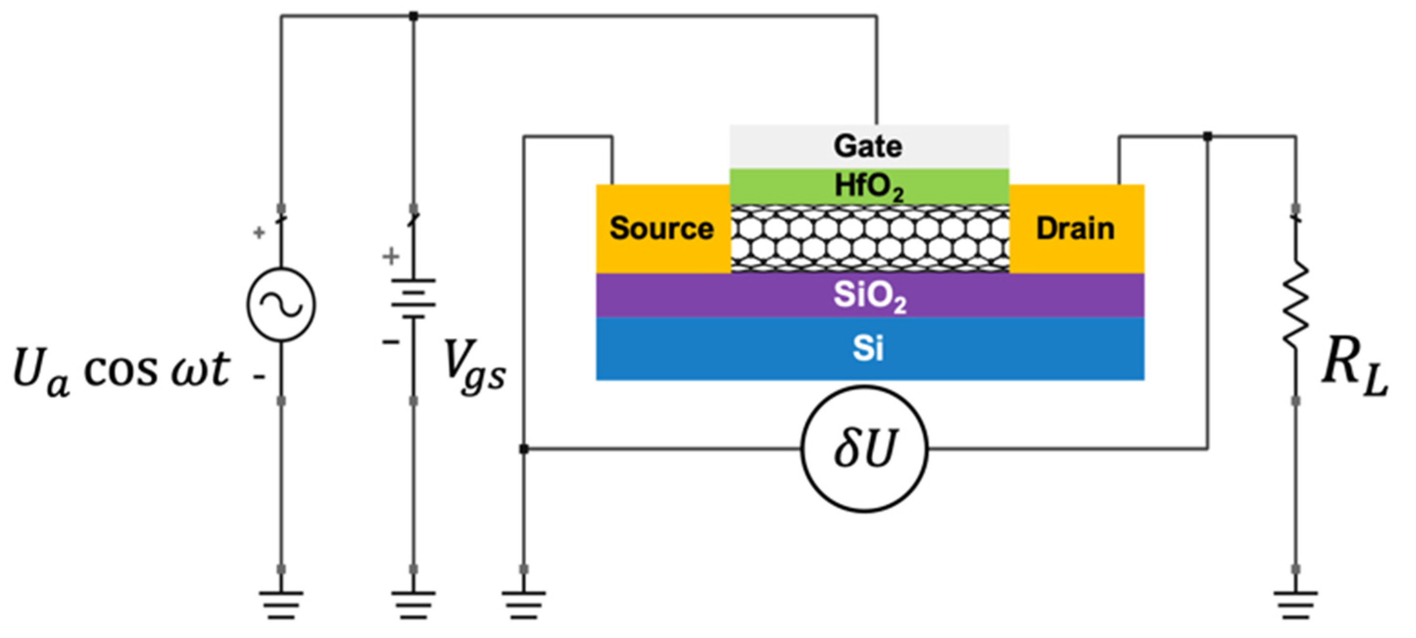
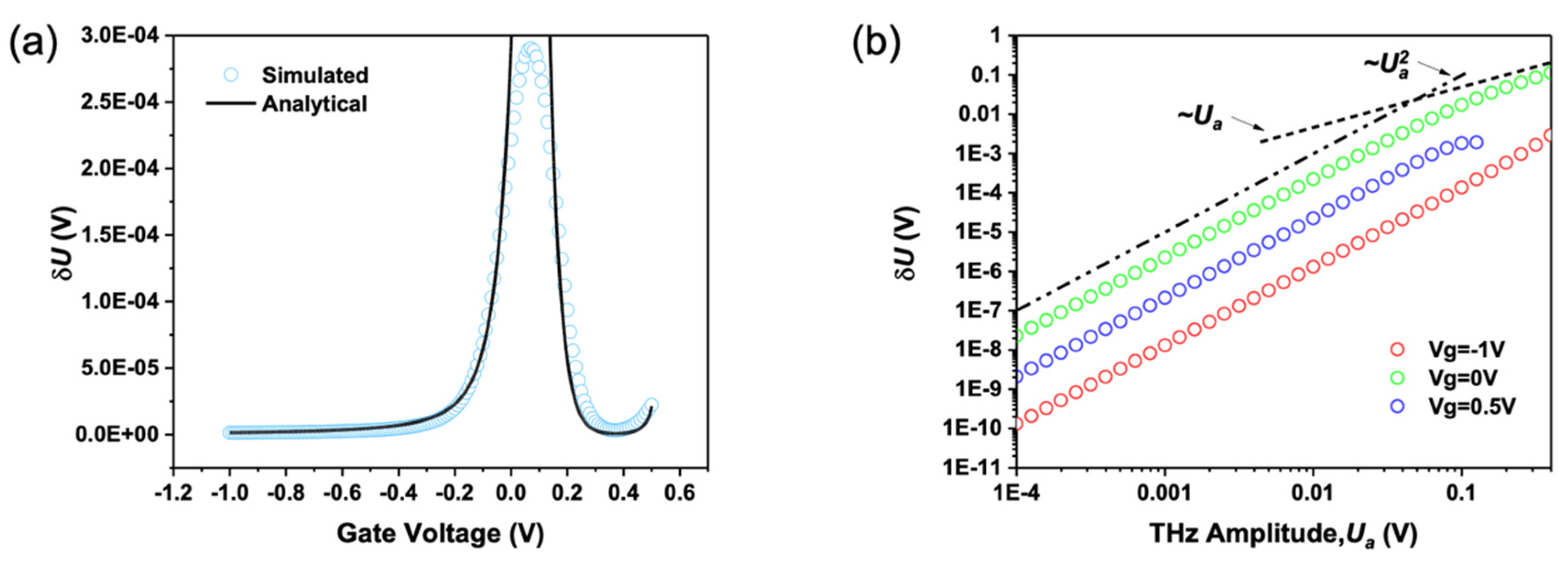
Figure 3 shows a schematic of the SPICE simulation circuit used for THz detection in the CNTFET with the load resistance of 2 at the drain. The load resistance effect can be described as where is the channel resistance and is the load resistance [24]. The induced AC signal between gate and source was modeled as the AC voltage source, and the THz response of the CNTFET was estimated by extracting the DC component of the drain response. The effect of the substrate was implicitly accounted for via the fitted current–voltage characteristics. The response was also analytically estimated on the basis of the broadband detector model [22,23,24]. Firstly, the drain response to 0.3 THz signaled as a function of the gate voltage with and the optimized external capacitances at 300 K was estimated. Figure 4a shows a good match between the analytical model and the simulated results in the above threshold regime, thus confirming that the proposed CNTFET model is valid for simulating THz detection. The drain response as a function of at different gate voltages was also simulated, as shown in Figure 4b. The quadratic response (~) corresponding to the non-resonant plasmon oscillations to the incident 0.3-THz signal was identified at positive, negative, and zero gate biases. Since at 0.3 THz in the tested gate voltage region, the non-resonant drain response was theoretically estimated [23,24]. The plasmonic response in the broad range of the gate voltages results from the ambipolar characteristics of the CNTFET. At a zero gate voltage, the quadratic response at small and the non-quadratic response at large were distinctly observed, as predicted by the analytical theory [25]. At a positive gate voltage, the response became saturated, and a relatively narrow range was shown. At a negative gate voltage, the broad dynamic range was identified, but response saturation was not observed in the tested range of . The simulated response at different gate voltages commonly increases quadratically as increases up to ~0.03 V, and this sufficiently wide dynamic range allows CNT THz detection.
4. CNTFET THz Spectrometer
Using the unified charge control CNTFET model with the optimized parameters above, we simulated the operation of the p-CNTFET spectrometer at the THz frequencies. A multisegment approach [26] was adopted in the present simulation to consider the current crowding effect. Fifty channel segments were used, allowing response simulation at high frequencies (up to 10 THz). The THz spectrometer response of p-diamond, GaN, InGaAs, and Si FET with asymmetry induced by the phase difference between the applied THz signals at the source and at the drain (Figure 5), was demonstrated in the earlier studies [26]. The response is given as follows [27]:
where is the phase difference; is the plasma wave vector; is the inverse momentum relaxation time; , the plasma wave velocity for the gated wire [28]; and is the effective mass of the charge carrier.
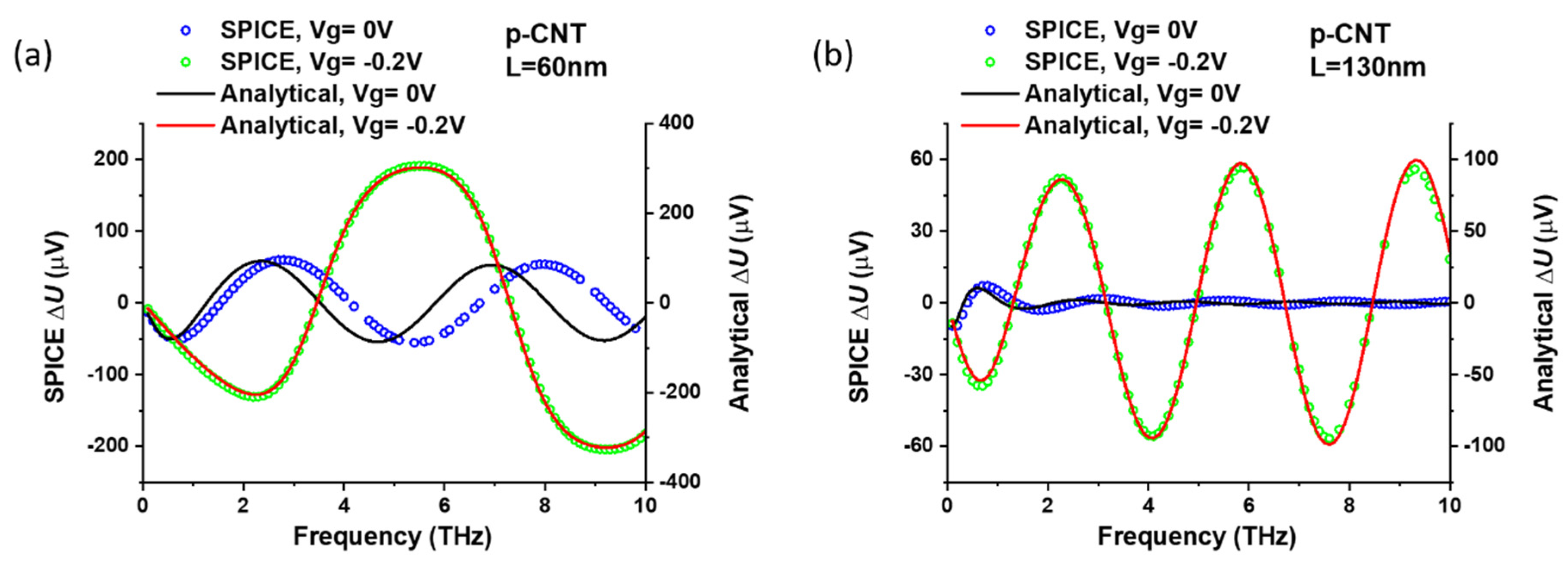
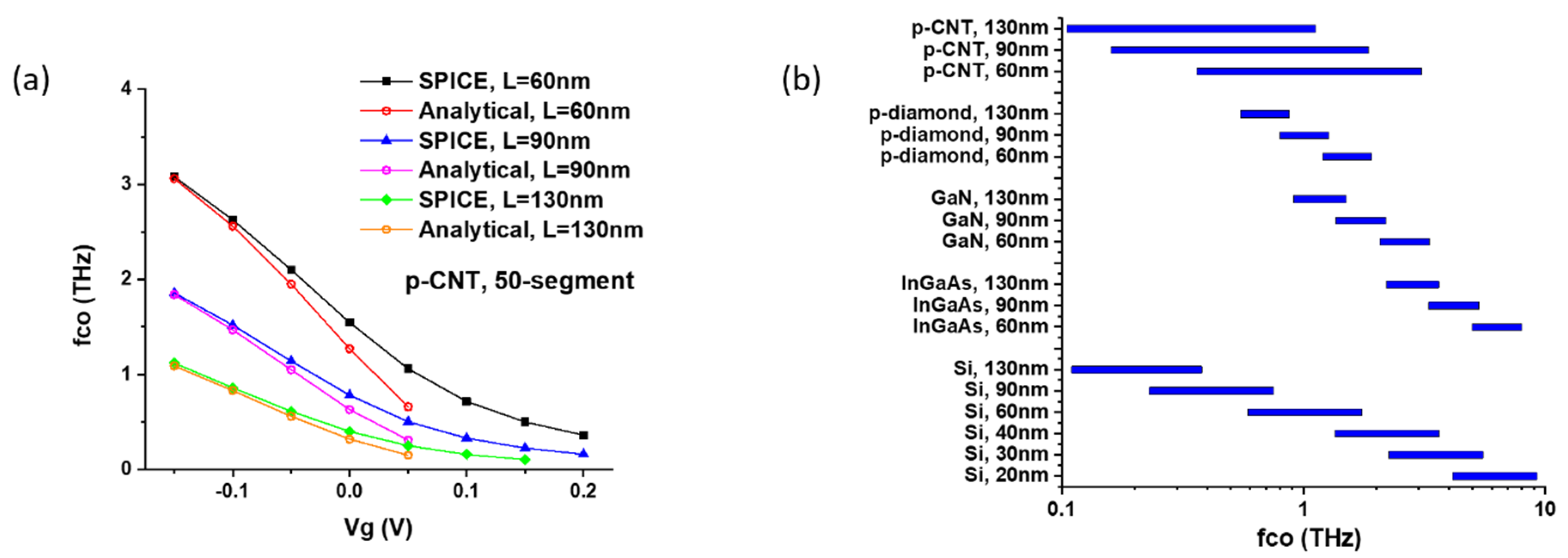
Figure 6a,b show the comparison between the analytical and simulated responses as a function of the frequency in the above threshold regime, and good agreement can be observed between them. The results demonstrate that the response of the spectrometer is periodic with the frequency even in the nonresonant condition, and it can be modulated by adjusting the gate bias and the channel length. An important feature of the spectrometer response is the characteristic frequencies, corresponding to the zero response, which are called cross-over frequencies [26,27]. Under incident radiation with a specific frequency, the lowest value of the cross-over frequencies, , can be tuned by the gate bias for each degree of the phase shift, and the range of with the specific phase shift is the critical parameter for the operation of the spectrometer [26].
Figure 7a shows comparison of the dependence of on the gate voltage between the analytical and simulated results for different CNT channel lengths. Figure 7b represents the ranges of in the p-CNTFET spectrometers with different channel lengths, which are compared with those in electronic devices based on different materials [26]. The p-CNTFET spectrometer shows the broad range of , and its operational frequency band covers a broad range from 0.1 to 3.08 THz.
5. Conclusions
In this report, we have proposed the compact unified charge control CNTFET model that consists of p-CNTFET and n-CNTFET connected in parallel to accurately estimate the performance of the ambipolar CNTFETs and investigated THz response behavior in the CNTFET using this compact model. The model has been validated by comparison between the SPICE simulations and measurements, confirming that the present model can describe the DC characteristics of the CNTFETs for the hole and electron conduction regime. The simulated drain voltage THz response depending on the gate bias closely agrees with the analytical results, thus demonstrating that our CNTFET model is valid for simulating the THz detection. Further simulation results confirm that the CNTFET detectors can operate in a wide range of incident beam power and gate bias. We have also demonstrated the operation of the CNTFET spectrometer in the THz frequency range using the proposed compact model with the multisegment approach. The results show that the gate voltage-tunable response of the CNTFET spectrometer covers wide range of frequencies from 0.1 to 3.08 THz. With increasing demand for high-speed wireless communications, the THz frequency range has become an essential bandwidth, also increasing the necessity for development of novel THz detectors. Carbon Nanotubes are a promising material for THz sensing, and our compact CNTFET model could be employed for investigating and developing the CNT-based THz devices.
Author Contributions
Conceptualization, M.S.; methodology, J.P. and T.Y.; software and validation, J.P. and X.L.; writing—original draft preparation, J.P.; writing—review and editing, X.L., T.Y. and M.S.; supervision, M.S. All authors have read and agreed to the published version of the manuscript.
Funding
This work at RPI was supported by the U.S. Army Research Laboratory under the Cooperative Research Agreement (Project Monitor Dr. Meredith Reed) and by the US ONR (Project Monitor Dr. Paul Maki).
Conflicts of Interest
The authors declare no conflict of interest.
References
- Hills, G.; Lau, C.; Wright, A.; Fuller, S.; Bishop, M.D.; Srimani, T.; Kanhaiya, P.; Ho, R.; Amer, A.; Stein, Y.; et al. Modern microprocessor built from complementary carbon nanotube transistors. Nature 2019, 572, 595–602. [Google Scholar] [CrossRef]
- Landauer, G.M.; González, J.L. Radio-frequency performance of carbon nanotube-based devices and circuits considering noise and process variation. IEEE Trans. Nanotechnol. 2014, 13, 228–237. [Google Scholar] [CrossRef]
- Guo, J.; Datta, S.; Lundstrom, M.; Brink, M.; McEuen, P.; Javey, A.; Dai, H.; Kim, H.; McIntyre, P. Assessment of silicon MOS and carbon nanotube FET performance limits using a general theory of ballistic transistors. In Proceedings of the Digest. International Electron Devices Meeting, San Francisco, CA, USA, 8–11 December 2002. [Google Scholar] [CrossRef]
- Natori, K.; Kimura, Y.; Shimizu, T. Characteristics of a carbon nanotube field-effect transistor analyzed as a ballistic nanowire field-effect transistor. J. Appl. Phys. 2005, 97, 034306. [Google Scholar] [CrossRef] [Green Version]
- Guo, J.; Datta, S.; Lundstrom, M. A numerical study of scaling issues for Schottky-barrier carbon nanotube transistors. IEEE Trans. Electron Devices 2004, 51, 172–177. [Google Scholar] [CrossRef] [Green Version]
- Raychowdhury, A.; Mukhopadhyay, S.; Roy, K. A circuit-compatible model of ballistic carbon nanotube field-effect transistors. IEEE Trans. Comput. Aided Design Integr. Circuits Syst. 2004, 23, 1411–1420. [Google Scholar] [CrossRef]
- Deng, J.; Wong, H.S.P. A compact SPICE model for carbon-nanotube field-effect transistors including nonidealities and its application—Part I: Model of the intrinsic channel region. IEEE Trans. Electron Devices 2007, 54, 3186–3194. [Google Scholar] [CrossRef]
- Deng, J.; Wong, H.S.P. A compact SPICE model for carbon-nanotube field-effect transistors including nonidealities and its application—Part II: Full device model and circuit performance benchmarking. IEEE Trans. Electron Devices 2007, 54, 3195–3205. [Google Scholar] [CrossRef]
- O’Connor, I.; Liu, J.; Gaffiot, F.; Prégaldiny, F.; Lallement, C.; Maneux, C.; Goguet, J.; Frégonèse, S.; Zimmer, T.; Anghel, L.; et al. CNTFET modeling and reconfigurable logic-circuit design. IEEE Trans. Circuits Syst. I 2007, 54, 2365–2379. [Google Scholar] [CrossRef]
- Frégonèse, S.; d’Honincthun, H.C.; Goguet, J.; Maneux, C.; Zimmer, T.; Bourgoin, J.-P.; Dollfus, P.; Galdin-Retailleau, S. Computationally efficient physics-based compact CNTFET model for circuit design. IEEE Trans. Electron Devices 2008, 55, 1317–1327. [Google Scholar] [CrossRef]
- Yang, X.; Mohanram, K. Modeling and performance investigation of the double-gate carbon nanotube transistor. IEEE Electron Device Lett. 2011, 32, 231–233. [Google Scholar] [CrossRef]
- Moon, B.-J.; Byun, Y.H.; Lee, K.; Shur, M. New continuous heterostructure field-effect-transistor model and unified parameter extraction technique. IEEE Trans. Electron Devices 1990, 37, 908–919. [Google Scholar] [CrossRef]
- Park, C.K.; Lee, C.Y.; Lee, K.; Moon, B.J.; Byun, Y.H.; Shur, M. A Unified Charge Control Model for Long Channel n-MOSFETs. IEEE Trans. Electron Devices 1991, 38, 399–406. [Google Scholar] [CrossRef]
- Lee, K.; Shur, M.S.; Fjeldly, T.A.; Ytterdal, T. Semiconductor Device Modeling for VLSI.; Prentice Hall: Englewood Cliffs, NJ, USA, 1993. [Google Scholar]
- Fjeldly, T.; Ytterdal, T.; Shur, M.S. Introduction to Device Modeling and Circuit Simulation for VLSI.; John Wiley and Sons: New York, NY, USA, 1998. [Google Scholar]
- Burke, P.J. An RF circuit model for carbon nanotubes. IEEE Trans. Nanotechnol. 2003, 2, 55–58. [Google Scholar] [CrossRef] [Green Version]
- Dürkop, T.; Getty, S.A.; Cobas, E.; Fuhrer, M.S. Extraordinary Mobility in Semiconducting Carbon Nanotubes. Nano Lett. 2004, 4, 35–39. [Google Scholar] [CrossRef]
- Meyer, J.E. MOS models and circuit simulation. RCA Rev. 1971, 32, 42–63. [Google Scholar]
- Javey, A.; Guo, J.; Farmer, D.B.; Wang, Q.; Yenilmez, E.; Gordon, R.G.; Lundstrom, M.; Dai, H. Self-Aligned Ballistic Molecular Transistors and Electrically Parallel Nanotube Arrays. Nano Lett. 2004, 4, 1319–1322. [Google Scholar] [CrossRef] [Green Version]
- Javey, A.; Guo, J.; Wang, Q.; Lundstrom, M.; Dai, H. Ballistic carbon nanotube field-effect transistors. Nature 2003, 424, 654–657. [Google Scholar] [CrossRef]
- Rosenblatt, S.; Yaish, Y.; Park, J.; Gore, J.; Sazonova, V.; McEuen, P.L. High performance electrolyte gated carbon nanotube transistors. Nano Lett. 2002, 2, 869–872. [Google Scholar] [CrossRef]
- Dyakonov, M.; Shur, M. Shallow water analogy for a ballistic field effect transistor: New mechanism of plasma wave generation by dc current. Phys. Rev. Lett. 1993, 71, 2465–2468. [Google Scholar] [CrossRef] [PubMed]
- Dyakonov, M.; Shur, M. Detection, mixing, and frequency multiplication of terahertz radiation by two-dimensional electronic fluid. IEEE Trans. Electron Devices 1996, 43, 380–387. [Google Scholar] [CrossRef]
- Liu, X.; Dovidenko, K.; Park, J.; Ytterdal, T.; Shur, M.S. Compact terahertz SPICE model: Effects of Drude inductance and leakage. IEEE Trans. Electron Devices 2018, 65, 5350–5356. [Google Scholar] [CrossRef]
- Gutin, A.; Kachorovskii, V.; Muraviev, A.; Shur, M. Plasmonic terahertz detector response at high intensities. J. Appl. Phys. 2012, 112, 014508. [Google Scholar] [CrossRef]
- Liu, X.; Ytterdal, T.; Shur, M. Plasmonic FET Terahertz Spectrometer. IEEE Access 2020, 8, 56039–56044. [Google Scholar] [CrossRef]
- Gorbenko, I.V.; Kachorovskii, V.Y.; Shur, M. Terahertz plasmonic detector controlled by phase asymmetry. Opt. Express 2019, 27, 4004–4013. [Google Scholar] [CrossRef] [Green Version]
- Shur, M.S.; Ryzhii, V. Plasma wave electronics. Int. J. High Speed Electron. Syst. 2003, 13, 575–600. [Google Scholar] [CrossRef]
Figure 1.
The equivalent circuit of the carbon nanotube field-effect transistor (CNTFET) SPICE model. The CNTFET can be modeled as parallel-connected n-type and p-type CNTFETs. and indicate the intrinsic gate-source capacitance and the gate-drain capacitance of the n-CNTFET (p-CNTFET), respectively.

Figure 2.
Measured [19] (symbols) and simulated (lines) drain currents for the CNTFET compact model. (a) Transfer characteristics at drain voltage, = −0.1, −0.2, and −0.3 V. (b) Output characteristics at the gate voltage, from −1.3 to 0.2 V in 0.3 steps.
Figure 2.
Measured [19] (symbols) and simulated (lines) drain currents for the CNTFET compact model. (a) Transfer characteristics at drain voltage, = −0.1, −0.2, and −0.3 V. (b) Output characteristics at the gate voltage, from −1.3 to 0.2 V in 0.3 steps.

Figure 3.
Schematic illustration of the simulation circuit for the CNTFET THz detection with the open boundary condition at the drain.
Figure 3.
Schematic illustration of the simulation circuit for the CNTFET THz detection with the open boundary condition at the drain.

Figure 4.
(a) Analytical (symbols) and simulated (solid line) THz responses to the 0.3 THz signal as a function of the gate voltage with a small amplitude (), (b) Simulated THz response versus the amplitude of radiation at and .
Figure 4.
(a) Analytical (symbols) and simulated (solid line) THz responses to the 0.3 THz signal as a function of the gate voltage with a small amplitude (), (b) Simulated THz response versus the amplitude of radiation at and .

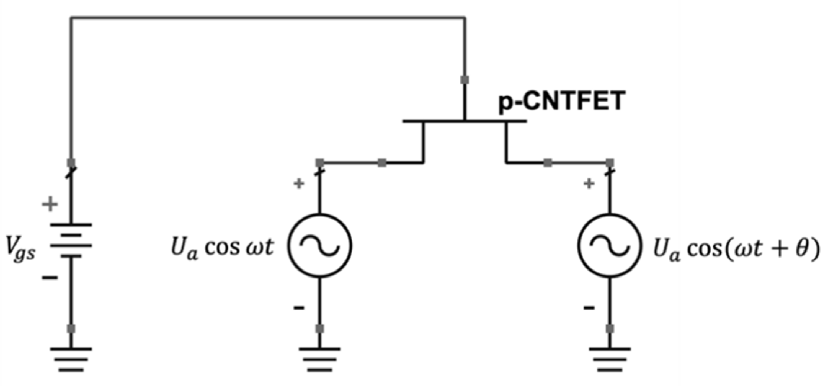
Figure 5.
Schematic simulation circuit for the p-CNTFET spectrometer. The THz rectification voltage response is generated due to the asymmetric boundary conditions induced by the phase shift, , between two THz signals applied to the source and drain at the gate bias, .
Figure 5.
Schematic simulation circuit for the p-CNTFET spectrometer. The THz rectification voltage response is generated due to the asymmetric boundary conditions induced by the phase shift, , between two THz signals applied to the source and drain at the gate bias, .

Figure 6.
Frequency dependent spectrometer response in the above threshold regime () for the p-CNTFET with (a) = 60 nm, and (b) = 130 nm.
Figure 6.
Frequency dependent spectrometer response in the above threshold regime () for the p-CNTFET with (a) = 60 nm, and (b) = 130 nm.

Figure 7.
(a) Gate-voltage dependent cross-over frequencies estimated from the simulated results and analytical model with different channel lengths of the p-CNTFET. (b) Cross-over frequency ranges in different material-based devices [26].
Figure 7.
(a) Gate-voltage dependent cross-over frequencies estimated from the simulated results and analytical model with different channel lengths of the p-CNTFET. (b) Cross-over frequency ranges in different material-based devices [26].

© 2020 by the authors. Licensee MDPI, Basel, Switzerland. This article is an open access article distributed under the terms and conditions of the Creative Commons Attribution (CC BY) license (http://creativecommons.org/licenses/by/4.0/).
Share and Cite
MDPI and ACS Style
Park, J.; Liu, X.; Ytterdal, T.; Shur, M. Carbon Nanotube Detectors and Spectrometers for the Terahertz Range. Crystals 2020, 10, 601. https://0-doi-org.brum.beds.ac.uk/10.3390/cryst10070601
AMA Style
Park J, Liu X, Ytterdal T, Shur M. Carbon Nanotube Detectors and Spectrometers for the Terahertz Range. Crystals. 2020; 10(7):601. https://0-doi-org.brum.beds.ac.uk/10.3390/cryst10070601
Chicago/Turabian StylePark, Junsung, Xueqing Liu, Trond Ytterdal, and Michael Shur. 2020. "Carbon Nanotube Detectors and Spectrometers for the Terahertz Range" Crystals 10, no. 7: 601. https://0-doi-org.brum.beds.ac.uk/10.3390/cryst10070601
Note that from the first issue of 2016, this journal uses article numbers instead of page numbers. See further details here.