Article

Light Output Enhancement of GaN-Based Light-Emitting Diodes Based on AlN/GaN Distributed Bragg Reflectors Grown on Si (111) Substrates

1
School of Materials and Energy, Guangdong University of Technology, Guangzhou 510006, China
2
College of Mechanical Engineering and Photoelectric Physics, Huaihua University, Huaihua 418000, China
*
Authors to whom correspondence should be addressed.
Submission received: 8 August 2020 / Revised: 27 August 2020 / Accepted: 31 August 2020 / Published: 1 September 2020
(This article belongs to the Special Issue Nitride Compound Light Emitting Diodes)

Abstract

:
Due to the absorption of opaque Si substrates, the luminous efficiency of GaN-based light-emitting diodes (LEDs) on Si substrates is not high. So, in this work, we insert AlN/GaN distributed Bragg reflectors (DBRs) to improve the light output of GaN-based LEDs on Si (111) substrates grown via metal organic chemical vapor deposition (MOCVD). In order to obtain the highest reflectivity of the AlN/GaN DBR stop band, the growth parameters of AlN/GaN DBRs are optimized, including the growth temperature, the V/III ratio and the growth pressure. As a consequence, the interfaces of the optimal 9-pair AlN/GaN DBRs become abrupt, and the reflectivity of the DBR stop band is as high as 85.2%, near to the calculated value (92.5%). Finally, crack-free GaN-based LEDs with 5-pair AlN/GaN DBRs are grown on Si (111) substrates. The light output of the DBR-based LED is evidently enhanced by 41.8% at the injection current of 350 mA, compared with the conventional DBR-based LED without DBRs. These results pave the way for the luminous efficiency improvement of future green and red GaN-based LEDs grown on Si substrates.

Graphical Abstract

1. Introduction

In the past two decades, III-Nitride DBRs have been applied in LEDs to improve the light output [1,2,3,4] or even in vertical-cavity surface-emitting lasers as resonant cavities [5]. Due to the important advantage in that III-Nitride DBRs can be fabricated by in situ epitaxy, many approaches have been adopted such as AlN/GaN [6,7,8,9,10], AlGaN/GaN [11,12], AlGaN/AlN [13,14,15,16], AlInN/GaN [17,18,19], AlInN/AlGaN [20,21] and so on. Among these III-Nitride DBRs, the AlN/GaN DBR structure has attracted most attention, because of the largest refractive index contrast between AlN (2.1) and GaN (2.4). Ive et al. deposited 20.5 periods of AlN/GaN DBRs on SiC substrates, which had a stop band width of 40~50 nm and a maximum measured reflectance of 99% [22]. Cai et al. deposited 25-pair AlN/GaN DBRs on sapphire with the reflectivity exceeding 90%, and the DBR-based LED showed a super-linear increase up to a current density of 135 A/cm2 and the relative external quantum efficiency (EQE) kept monotonously increasing with the increase in injection current density [3]. Mastro et al. grew 5-pair AlN/GaN DBRs with the peak reflectivity of 69.8% on Si substrates, while the LED structure was not deposited [23]. Among these substrates (SiC, sapphire and Si) for III-Nitrides heteroepitaxy, it is most difficult to deposit III-Nitride DBRs and GaN-based LEDs on Si, due to the tensile stress caused by the large mismatch of the thermal expansion coefficient between GaN and Si. On the other hand, Si substrates are the lowest cost and they provide opportunities for optoelectronic integration. Thus, it is very important to insert III-Nitride DBRs in situ between the LED active layer and the Si substrate, since the light emitted downwards would be reflected by the DBR and prevented from being absorbed by the opaque Si substrate [24]. Then, the luminous efficiency of LEDs on Si substrates can be improved. However, there are very few reports about GaN-based LEDs on Si substrates with III-Nitride DBRs. Ishikawa et al. achieved crack-free DBR-based LEDs on Si with only 3-pair AlGaN/AlN DBR structures, resulting in an improvement of light output power [25]. However, the light output decreased when increasing DBRs to five pairs because of a crack formation.
In this work, in order to obtain the highest reflectivity of DBRs, the AlN/GaN DBRs with the largest refractive index contrast are grown on Si (111) substrates, and the growth parameters of AlN/GaN DBRs are optimized, including the growth temperature, the V/III ratio and the growth pressure. It is found that the optimal growth conditions for AlN/GaN DBRs are growth temperature of 1020 °C, V/III ratio of 2500 and growth pressure of 70 mbar. As a result, the interfaces of the optimized 9-pair AlN/GaN DBRs become abrupt and the maximum reflectivity reaches 85.2%, near to the calculated value (92.5%). Finally, crack-free GaN-based LEDs with 5-pair AlN/GaN DBRs are grown on Si (111) substrates. In comparison with those conventional LEDs without DBRs, the AlN/GaN DBR-based LEDs show a light output enhancement of 41.8%, at the injection current of 350 mA.

2. Materials and Methods

Epitaxial layers on 2″ Si (111) substrates were deposited in the MOCVD system (Aixtron, Thomas Swan 3x2FT system, Herzogenrath, Germany). In order to eliminate the desorption of AlN or GaN layers during the growth of AlN/GaN DBRs and control their thickness precisely, AlN and GaN of these DBRs were grown at the same condition during each growth and their interval time was as short as 10 s. The thickness of AlN and GaN was 55 and 48 nm, corresponding to the stop band center of 460 nm. The epitaxial structure of these 9-pair AlN/GaN DBRs with a 300-nm GaN cap layer is shown in Figure 1a. There are three series of the 9-pair AlN/GaN DBRs, named series A, B and C. For series A, the growth pressure and the V/III ratio of AlN/GaN DBRs remained at 100 mbar and 2500, while the growth temperature was varied at 1000 °C (sample A1), 1020 °C (sample A2), 1040 °C (sample A3) and 1060 °C (sample A4). For series B, the growth temperature and pressure of AlN/GaN DBRs remained at 1060 °C and 100 mbar, while the V/III ratio was varied at 500 (sample B1), 1000 (sample B2), 1500 (sample B3) and 2500 (sample B4). For series C, the growth temperature and the V/III ratio of AlN/GaN DBRs remained at 1060 °C and 2500, while the growth pressure was varied at 70 mbar (sample C1), 100 mbar (sample C2), 130 mbar (sample C3) and 160 mbar (sample C4). Finally, owing to the stress compensation of the 660-nm compositionally graded AlGaN buffer layer [26], crack-free GaN-based LEDs with 5-pair AlN/GaN DBRs were grown on Si (111) substrates, consisting of 800 nm n-GaN, 6-pair InGaN/GaN multiple quantum wells and 240 nm p-GaN, as shown in Figure 1b. As a reference, non DBR-based LEDs on Si were also fabricated, and these two types of LED samples are classified into series D. Reflectivity, SEM images, TEM images and EL spetrum were measured by the spectrophotometer (Shimadzu, UV-3600Plus, Kyoto, Japan), the SEM (Hitachi, SU8220, Tokyo, Japan), the TEM (FEI, Talos F200S, Hillsboro, OR, USA) and the optical spectrum analyzer (Yokogawa, AQ6373, Tokyo, Japan), respectively.

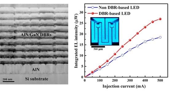
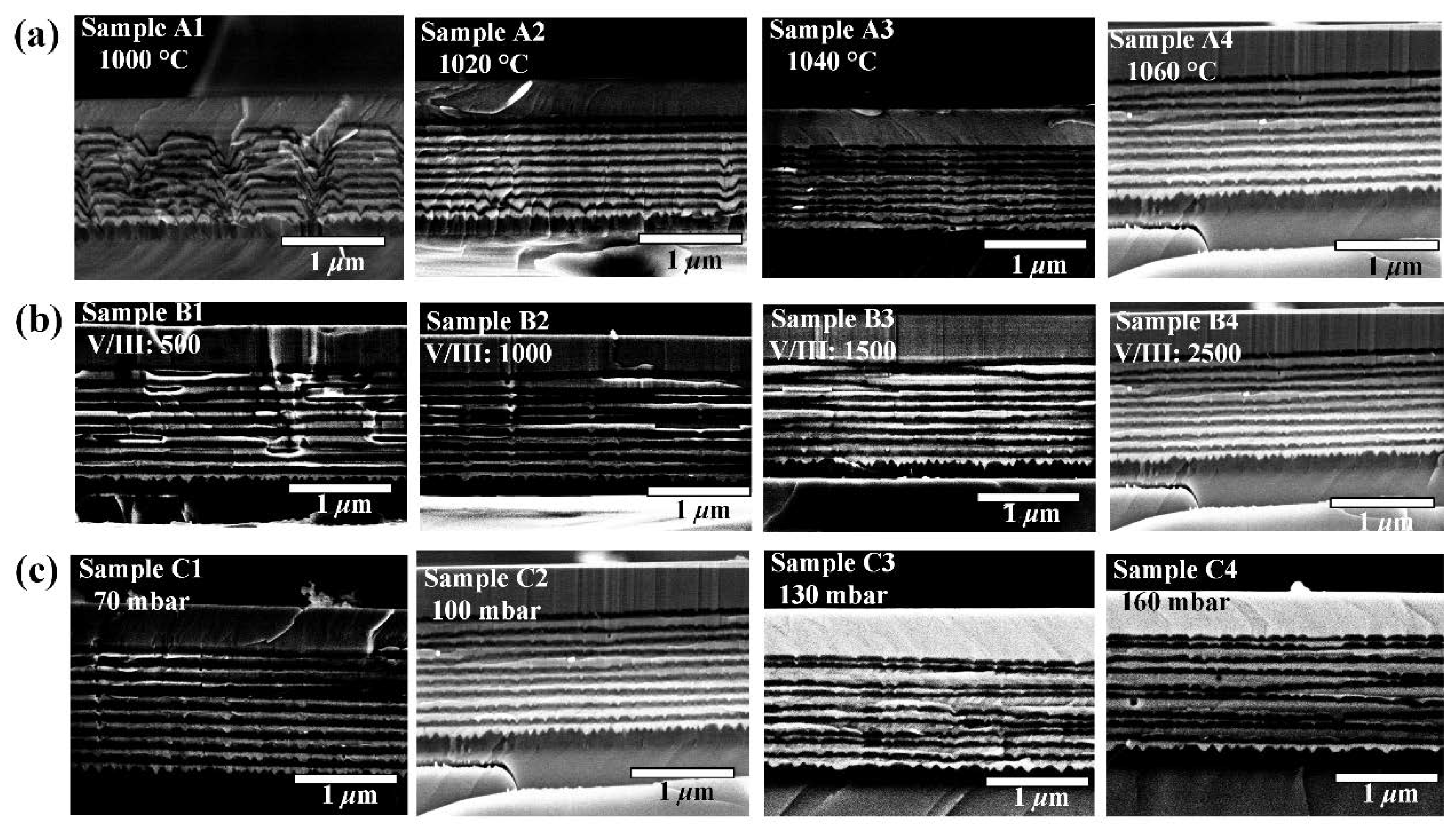
3. Results and Discussion

The temperature-dependent reflectivity of the AlN/GaN DBR stop band of series A is exhibited in Figure 2a. It is clear that the reflectivity is the lowest at the growth temperature of 1000 °C. Then, the reflectivity reaches the highest when the growth temperature rises to 1020 °C. However, when the growth temperature continues to increase to 1040 and 1060 °C, the reflectivity decreases. In order to find the reasons, cross-sectional SEM images of AlN/GaN DBR interfaces are illustrated in Figure 3a. It is found that the AlN/GaN DBR interfaces are very rough and many big V-type defects appear at the growth temperature of 1000 °C. When the growth temperature increases to 1020 °C, the interfaces become much smoother. When further increasing the growth temperature to 1040 and 1060 °C, the smoothness of the interfaces is a little degraded. These SEM results confirm the reflectivity measurement. The reason is that a too low growth temperature would result in the 3D growth of AlN and GaN, which causes rough interfaces [27,28]. On the other hand, a too high growth temperature would lead to the desorption of GaN, which degrades the smoothness of AlN/GaN interfaces [28,29].
The reflectivity versus V/III ratio of series B is depicted in Figure 2b. It is obvious that the reflectivity increases with the increase in the V/III ratio of AlN/GaN DBRs, while it tends to be saturated at the value of 2500. Figure 3b displays the corresponding cross-sectional SEM images of the AlN/GaN DBR interfaces of series B. It can be seen that the interfaces are very rough at the V/III ratio of 500 while they become quite flat at the V/III ratio of 2500, which indicates that the smoothness of AlN/GaN interfaces is improved with the increase in V/III ratio. These results agree with the measurement of reflectivity. This is because the higher V/III ratio improves the surface mobility of Ga (Al) atoms, which promotes the two-dimensional (2D) growth of GaN (AlN) films [30,31,32], whereas the lower V/III ratio reduces the surface mobility of Ga (Al) atoms, which results in the three-dimensional (3D) growth of GaN (AlN) films and rough interfaces of AlN/GaN DBRs.
Figure 2c exhibits the reflectivity as a function of growth pressure of series B. It is obviously seen that the reflectivity decreases distinctly when increasing the growth pressure of AlN/GaN DBRs from 70 to 160 mbar. The reason can be found in the cross-sectional SEM images of AlN/GaN interfaces, as shown in Figure 3c. When the growth pressure is 70 mbar, the thickness of GaN (AlN) films is uniform and the interfaces are very sharp. However, when the growth pressure is 130 or 160 mbar, the thickness of GaN (AlN) films fluctuates visibly, which leads to the roughness of AlN/GaN interfaces and the low reflectivity. Therefore, this indicates that the lower growth pressure facilitates the 2D growth of GaN (AlN) films and thereby results in sharp interfaces of AlN/GaN DBRs and higher reflectivity, and vice versa [27].
Therefore, the optimized growth parameters of AlN/GaN DBRs are a growth temperature of 1020 °C, V/III ratio of 2500 and growth pressure of 70 mbar. The experimental and calculated reflectivity of the optimized 9-pair AlN/GaN DBRs are exhibited in Figure 4a. It can be seen that the experimental curve fits the calculated one quite well. The reflectivity of the DBR stop band is 85.2%, which is close to the calculated value (92.5%). Cross-sectional TEM images of AlN/GaN DBRs are shown in Figure 4b. It is observed that the interface occurs abruptly when GaN is grown on AlN, but gradually in reverse order. This is caused by the compositional pulling effect when AlN is grown on compressed GaN [33]. Ga atoms move into AlN during the growth, which results in a graded AlGaN layer. Meanwhile, it can be seen that V-type pits occur in the AlN layer, which may result from the lower mobility of Al atoms or microcracks of AlN caused by tensile stress. All these factors would degrade the interfaces of AlN/GaN DBRs and reduce the reflectivity.
Figure 5 shows the calculated and experimental reflectivity of 9-pair AlN/GaN DBRs under different incident angles. The experimental results are in good agreement with the calculated results. With the increase in incident angles, the DBR stop band shows a blue shift and the reflectivity has a slight decrease, which is due to the reduction of the optical path. On the other hand, the critical angle of GaN-based LEDs is arcsin (1/nGaN) = 24.6°, where nGaN is the refractive index of GaN (2.4). Since the critical angle is quite small, the DBRs still have the ability to significantly improve the light output of LEDs in the light output direction.
Finally, LED samples in series D are fabricated, with the LED chip size of 1 mm × 1 mm. Figure 6a,b illustrate the electroluminescence (EL) spectrum of the non-DBR-based and the DBR-based LEDs at different injection currents, which is measured by an optical spectrum analyzer through an optical fiber at the near-top of the LED chip. This indicates that the EL intensity of the DBR-based LED is evidently improved at each injection current, compared with the non-DBR-based LED. To further quantify the enhancement of the light output, the integrated EL intensity is carried out, as shown in Figure 6c. The light output (integrated EL intensity) of the DBR-based LED is enhanced by 41.8% at the injection current of 350 mA (operating current).

4. Conclusions

In summary, we insert AlN/GaN DBRs to enhance the light output of GaN-based LEDs on Si (111) substrates by MOCVD. The growth parameters of AlN/GaN DBRs are optimized, including the growth temperature, the V/III ratio and the growth pressure. As a consequence, the reflectivity of the DBR stop band of the optimal 9-pair AlN/GaN DBRs is as high as 85.2%, near to the calculated value (92.5%). Finally, crack-free GaN-based LEDs with 5-pair AlN/GaN DBRs are grown on Si (111) substrates. The light output of the DBR-based LED is evidently improved, and it is enhanced by 41.8% at the injection current of 350 mA, in comparison with the conventional non-DBR-based LED. These results pave the way for the luminous efficiency improvement of future green and red GaN-based LEDs grown on Si substrates.

Author Contributions

Conceptualization, Y.Y.; data curation, Y.Y. and L.Z.; formal analysis, L.Z. and Y.Z.; funding acquisition, L.Z. and Y.Z.; investigation, Y.Y. and L.Z.; methodology, Y.Y. and L.Z.; writing—original draft, Y.Y.; writing—review and editing, L.Z. and Y.Z. All authors have read and agreed to the published version of the manuscript.

Funding

This research was funded by the National Natural Science Foundation of China (Grant No. 61975036) and the Science Research Foundation of Education Department of Hunan Province (No. 17C1264).

Acknowledgments

The authors would like to acknowledge the guidance of Baijun Zhang.

Conflicts of Interest

The authors declare no conflict of interest.

References

  1. Byrne, D.; Natali, F.; Damilano, B.; Dussaigne, A.; Grandjean, N.; Massies, J. Blue Resonant Cavity Light Emitting Diodes with a High-Al-Content GaN/AlGaN Distributed Bragg Reflector. Jpn. J. Appl. Phys. 2003, 42, L1509–L1511. [Google Scholar] [CrossRef]
  2. Ishikawa, H.; Zhang, B.; Asano, K.; Egawa, T.; Jimbo, T. Characterization of GaInN light-emitting diodes with distributed Bragg reflector grown on Si. J. Cryst. Growth 2004, 272, 322–326. [Google Scholar] [CrossRef]
  3. Cai, L.-E.; Zhang, B.-P.; Zhang, J.-Y.; Wu, C.-M.; Jiang, F.; Hu, X.-L.; Chen, M.; Wang, Q.-M. Improvement of efficiency droop of GaN-based light-emitting devices by a rear nitride reflector. Phys. E 2010, 43, 289–292. [Google Scholar] [CrossRef]
  4. Wen, F.; Huang, L.; Jiang, B.; Tong, L.; Xu, W.; Liu, D. Near white light emission from GaN based light emitting diode with GaN/AlGaN distributed Bragg reflector. Mater. Sci. Semicond. Process. 2010, 13, 147–150. [Google Scholar] [CrossRef]
  5. Sari, E.; Nizamoglu, S.; Ozel, T.; Demir, H.V. Blue quantum electroabsorption modulators based on reversed quantum confined Stark effect with blueshift. Appl. Phys. Lett. 2007, 90, 011101. [Google Scholar] [CrossRef]
  6. Yao, H.H.; Lin, C.F.; Kuo, H.C.; Wang, S.C. MOCVD growth of AlN/GaN DBR structures under various ambient conditions. J. Cryst. Growth 2004, 262, 151–156. [Google Scholar] [CrossRef]
  7. Ive, T.; Brandt, O.; Ploog, K.H. Conductive and crack-free AlN/GaN:Si distributed Bragg reflectors grown on 6H-SiC(0001). J. Cryst. Growth 2005, 278, 355–360. [Google Scholar] [CrossRef]
  8. Mastro, M.A.; Holm, R.T.; Bassim, N.D.; Gaskill, D.K.; Culbertson, J.C.; Fatemi, M.; Eddy, C.R.; Henry, R.L.; Twigg, M.E. Metal-organic chemical-vapor deposition of high-reflectance III-nitride distributed Bragg reflectors on Si substrates. J. Vac. Sci. Technol. A 2006, 24, 1631. [Google Scholar] [CrossRef]
  9. Wu, C.M.; Zhang, B.P.; Shang, J.Z.; Cai, L.E.; Zhang, J.Y.; Yu, J.Z.; Wang, Q.M. High-reflectivity AlN/GaN distributed Bragg reflectors grown on sapphire substrates by MOCVD. Semicond. Sci. Technol. 2011, 26, 055013. [Google Scholar] [CrossRef]
  10. Gačević, Z.; Eljarrat, A.; Peiró, F.; Calleja, E. Insight into high-reflectivity AlN/GaN Bragg reflectors with spontaneously formed (Al,Ga)N transient layers at the interfaces. J. Appl. Phys. 2013, 113, 183106. [Google Scholar] [CrossRef]
  11. Dartsch, H.; Figge, S.; Aschenbrenner, T.; Pretorius, A.; Rosenauer, A.; Hommel, D. Strain compensated AlGaN/GaN-Bragg-reflectors with high Al content grown by MOVPE. J. Cryst. Growth 2008, 310, 4923–4926. [Google Scholar] [CrossRef]
  12. Wang, D.; Liang, H.; Tao, P.; Zhang, K.; Song, S.; Liu, Y.; Xia, X.; Shen, R.; Du, G. Crack-free ultraviolet AlGaN/GaN distributed Bragg reflectors grown by MOVPE on 6H-SiC(0001). Superlattices Microstruct. 2014, 70, 54–60. [Google Scholar] [CrossRef]
  13. Xie, Z.L.; Zhang, R.; Liu, B.; Ji, X.L.; Li, L.; Liu, C.X.; Jiang, R.L.; Gong, H.M.; Zhao, H.; Han, P.; et al. High reflectivity AlGaN/AlN DBR mirrors grown by MOCVD. J. Cryst. Growth 2007, 298, 691–694. [Google Scholar] [CrossRef]
  14. Chen, J.; Ling, S.; Hung, C.; Ko, T.; Lu, T.; Kuo, H.; Wang, S. High-reflectivity ultraviolet AlN/AlGaN distributed Bragg reflectors grown by metalorganic chemical vapor deposition. J. Cryst. Growth 2008, 310, 4871–4875. [Google Scholar] [CrossRef]
  15. Ji, X.L.; Jiang, R.L.; Liu, B.; Xie, Z.L.; Zhou, J.J.; Li, L.; Han, P.; Zhang, R.; Zheng, Y.D.; Zheng, J.G. Structural characterization of AlGaN/AlN Bragg reflector grown by metalorganic chemical vapor deposition. Phys. Status Solidi A 2008, 205, 1572–1574. [Google Scholar] [CrossRef]
  16. Liu, B.; Zhang, R.; Zheng, J.G.; Ji, X.L.; Fu, D.Y.; Xie, Z.L.; Chen, D.J.; Chen, P.; Jiang, R.L.; Zheng, Y.D. Composition pulling effect and strain relief mechanism in AlGaN/AlN distributed Bragg reflectors. Appl. Phys. Lett. 2011, 98, 261916. [Google Scholar] [CrossRef]
  17. Ishikawa, H.; Jimbo, T.; Egawa, T. GaInN light emitting diodes with AlInN/GaN distributed Bragg reflector on Si. Phys. Status Solidi C 2008, 5, 2086–2088. [Google Scholar] [CrossRef]
  18. Krost, A.; Berger, C.; Bläsing, J.; Franke, A.; Hempel, T.; Dadgar, A.; Christen, J. Strain evaluation in AlInN/GaN Bragg mirrors by in situ curvature measurements and ex situ x-ray grazing incidence and transmission scattering. Appl. Phys. Lett. 2010, 97, 181105. [Google Scholar] [CrossRef]
  19. Cosendey, G.; Carlin, J.-F.; Kaufmann, N.A.K.; Butté, R.l.; Grandjean, N. Strain compensation in AlInN/GaN multilayers on GaN substrates: Application to the realization of defect-free Bragg reflectors. Appl. Phys. Lett. 2011, 98, 181111. [Google Scholar] [CrossRef]
  20. Feltin, E.; Carlin, J.F.; Dorsaz, J.; Christmann, G.; Butté, R.; Laügt, M.; Ilegems, M.; Grandjean, N. Crack-free highly reflective AlInN/AlGaN Bragg mirrors for UV applications. Appl. Phys. Lett. 2006, 88, 051108. [Google Scholar] [CrossRef]
  21. Berger, C.; Dadgar, A.; Bläsing, J.; Krost, A. In-situ growth monitoring of AlInN/AlGaN distributed Bragg reflectors for the UV-spectral range. J. Cryst. Growth 2013, 370, 87–91. [Google Scholar] [CrossRef]
  22. Ive, T.; Brandt, O.; Kostial, H.; Hesjedal, T.; Ramsteiner, M.; Ploog, K.H. Crack-free and conductive Si-doped AlN/GaN distributed Bragg reflectors grown on 6H-SiC(0001). Appl. Phys. Lett. 2004, 85, 1970. [Google Scholar] [CrossRef] [Green Version]
  23. Mastro, M.A.; Holm, R.T.; Bassim, N.D.; Eddy, C.R.; Henry, R.L.; Twigg, M.E.; Rosenberg, A. Wurtzite III-Nitride Distributed Bragg Reflectors on Si(100) Substrates. Jpn. J. Appl. Phys. 2006, 45, L814–L816. [Google Scholar] [CrossRef]
  24. Lei, Y.; Wan, H.; Tang, B.; Lan, S.; Miao, J.; Wan, Z.; Liu, Y.; Zhou, S. Optical Characterization of GaN-Based Vertical Blue Light-Emitting Diodes on P-Type Silicon Substrate. Crystals 2020, 10, 621. [Google Scholar] [CrossRef]
  25. Ishikawa, H.; Asano, K.; Zhang, B.; Egawa, T.; Jimbo, T. Improved characteristics of GaN-based light-emitting diodes by distributed Bragg reflector grown on Si. Phys. Status Solidi A 2004, 201, 2653–2657. [Google Scholar] [CrossRef]
  26. Yang, Y.; Xiang, P.; Liu, M.; Chen, W.; He, Z.; Han, X.; Ni, Y.; Yang, F.; Yao, Y.; Wu, Z.; et al. Effect of compositionally graded AlGaN buffer layer grown by different functions of trimethylaluminum flow rates on the properties of GaN on Si (111) substrates. J. Cryst. Growth 2013, 376, 23–27. [Google Scholar] [CrossRef]
  27. Hiramatsu, K.; Nishiyama, K.; Onishi, M.; Mizutani, H.; Narukawa, M.; Motogaito, A.; Miyake, H.; Iyechika, Y.; Maeda, T. Fabrication and characterization of low defect density GaN using facet-controlled epitaxial lateral overgrowth (FACELO). J. Cryst. Growth 2000, 221, 316–326. [Google Scholar] [CrossRef]
  28. Koukitu, A.; Kumagai, Y. Thermodynamic analysis of group III nitrides grown by metal-organic vapour-phase epitaxy (MOVPE), hydride (or halide) vapour-phase epitaxy (HVPE) and molecular beam epitaxy (MBE). J. Phys. Condens. Matter 2001, 13, 6907–6934. [Google Scholar] [CrossRef]
  29. Koukitu, A.; Mayumi, M.; Kumagai, Y. Surface polarity dependence of decomposition and growth of GaN studied using in situ gravimetric monitoring. J. Cryst. Growth 2002, 246, 230–236. [Google Scholar] [CrossRef]
  30. Eddy, C.R.; Holm, R.T.; Henry, R.L.; Culbertson, J.C.; Twigg, M.E. Investigation of three-step epilayer growth approach of GaN films to minimize compensation. J. Electron. Mater. 2005, 34, 1187–1192. [Google Scholar] [CrossRef]
  31. Sengupta, D.; Mazumder, S.; Kuykendall, W.; Lowry, S.A. Combined ab initio quantum chemistry and computational fluid dynamics calculations for prediction of gallium nitride growth. J. Cryst. Growth 2005, 279, 369–382. [Google Scholar] [CrossRef]
  32. Yang, T.; Uchida, K.; Mishima, T.; Kasai, J.; Gotoh, J. Control of Initial Nucleation by Reducing the V/III Ratio during the Early Stages of GaN Growth. Phys. Status Solidi A 2000, 180, 45–50. [Google Scholar] [CrossRef]
  33. Chen, Z.; Pei, Y.; Newman, S.; Brown, D.; Chung, R.; Keller, S.; DenBaars, S.P.; Nakamura, S.; Mishra, U.K. Growth of AlGaN/GaN/AlGaN double heterojunction field-effect transistors and the observation of a compositional pulling effect. Appl. Phys. Lett. 2009, 94, 171117. [Google Scholar] [CrossRef]
Figure 1. Structures of (a) samples with 9-pair AlN/GaN distributed Bragg reflectors (DBRs) and (b) LEDs with 5-pair AlN/GaN DBRs.
Crystals 10 00772 g001
Figure 2. The reflectivity of the AlN/GaN DBR stop band of (a) series A, (b) series B and (c) series C.
Crystals 10 00772 g002
Figure 3. Cross-sectional SEM images of (a) series A, (b) series B and (c) series C.
Crystals 10 00772 g003
Figure 4. (a) The experimental and calculated reflectivity and (b) cross-sectional TEM images of the optimized 9-pair AlN/GaN DBRs.
Crystals 10 00772 g004
Figure 5. (a) The calculated and (b) experimental reflectivity of 9-pair AlN/GaN DBRs under different incident angles.
Crystals 10 00772 g005
Figure 6. Electroluminescence (EL) spectrum of (a) the non-DBR-based and (b) the DBR-based LEDs at different injection currents. (c) Integrated EL intensity (light output) of the DBR-based and the non-DBR-based LEDs, with an insert of a DBR-based LED chip with the size of 1 mm × 1 mm.
Crystals 10 00772 g006

