Development of Catalytic-CVD SiNx Passivation Process for AlGaN/GaN-on-Si HEMTs


1
Department of Electrical and Computer Engineering, Seoul National University, Seoul 08826, Korea
2
School of Electronic and Electrical Engineering, Hongik University, Seoul 04066, Korea
*
Author to whom correspondence should be addressed.
Crystals 2020, 10(9), 842; https://0-doi-org.brum.beds.ac.uk/10.3390/cryst10090842
Submission received: 23 August 2020
/
Revised: 16 September 2020
/
Accepted: 19 September 2020
/
Published: 21 September 2020
(This article belongs to the Special Issue Nano/Micro and Bio-Inspired Materials on Wide-Bandgap-Semiconductor-Based Optoelectronic/Power Devices)
Abstract
:We optimized a silicon nitride (SiNx) passivation process using a catalytic-chemical vapor deposition (Cat-CVD) system to suppress the current collapse phenomenon of AlGaN/GaN-on-Si high electron mobility transistors (HEMTs). The optimized Cat-CVD SiNx film exhibited a high film density of 2.7 g/cm3 with a low wet etch rate (buffered oxide etchant (BOE) 10:1) of 2 nm/min and a breakdown field of 8.2 MV/cm. The AlGaN/GaN-on-Si HEMT fabricated by the optimized Cat-CVD SiNx passivation process, which had a gate length of 1.5 μm and a source-to-drain distance of 6 μm, exhibited the maximum drain current density of 670 mA/mm and the maximum transconductance of 162 mS/mm with negligible hysteresis. We found that the optimized SiNx film had positive charges, which were responsible for suppressing the current collapse phenomenon.
1. Introduction
AlGaN/GaN high electron mobility transistors (HEMTs) are promising candidates for microwave power amplification and power switching applications owing to their excellent characteristics, such as wide energy bandgap, as well as high breakdown field, mobility, and saturation velocity [1,2]. Although significant progress has been achieved in the past decades, surface trapping and its related current collapse phenomena remain critical for device performance and reliability. The current collapse phenomenon that degrades the dynamic characteristics of the device contributes significantly to performance instability and reliability of the device. The current collapse phenomenon can be mitigated by surface passivation along with a field plate where the dielectric passivation process is carefully optimized [3]. Among the various dielectric materials, including SiO2, silicon nitride (SiNx), SiON, Al2O3, and AlN [4,5,6,7], SiNx films have been used frequently for the passivation layer of GaN FETs and have been reported to be effective for suppressing the current collapse phenomenon [8,9]. Various deposition systems have been utilized for SiNx film deposition, including plasma-enhanced chemical vapor deposition (PECVD), inductively coupled plasma CVD (ICP-CVD), and low-pressure CVD (LPCVD). These systems employ high-power plasma and/or a high deposition temperature causing plasma damage at the surface and thermal budget problems. Therefore, a catalytic CVD (Cat-CVD) process was proposed to solve these problems. The molecules of the source gases are decomposed in a vacuum chamber by catalytic cracking reaction using heated catalyzers without plasma reaction and then the cracked species are transported to the substrates to form a film [10,11,12,13].
In this study, we determined high-quality SiNx deposition process conditions using a Cat-CVD system. It was found that the optimized SiNx passivation process was very effective in reducing the interface trap density and, thus, successfully suppressed the current collapse phenomenon, thereby improving the device performance.
2. Experimental Details
2.1. Optimization of Cat-CVD SiNx Deposition Process
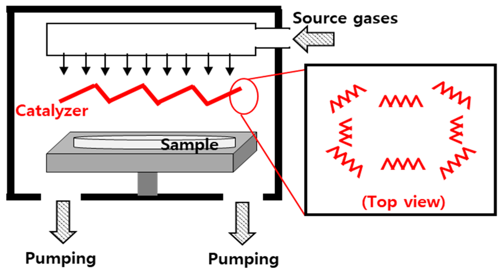
The Cat-CVD system used in this work is illustrated in Figure 1 where a tungsten wire with a diameter of 0.7 mm was used as a catalyzer located at a distance of ~70 mm apart from the substrate. Catalyzers were placed in an octagon between the gas injection and the substrate, and the full length was ~2.9 m. The catalyzer temperature was monitored by the resistance of the tungsten wire.
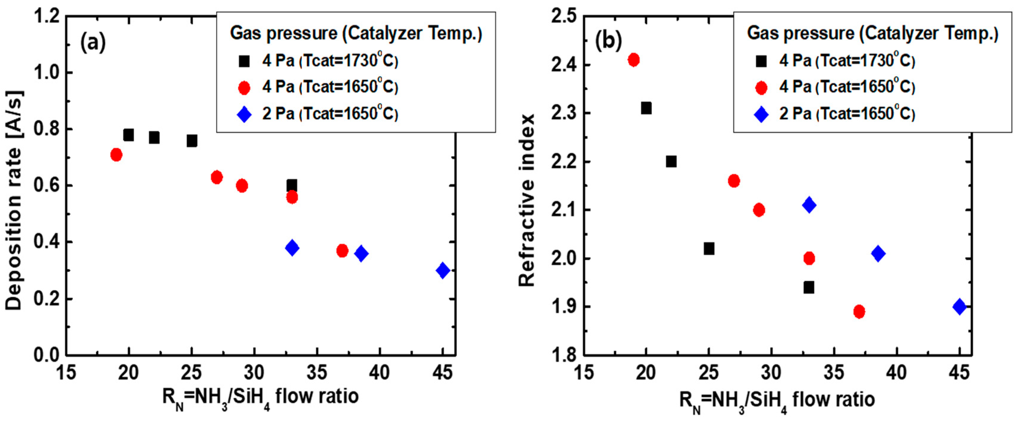
To optimize the SiNx deposition process, the films were deposited on Si wafers using a Cat-CVD system with SiH4 and NH3 gas mixtures, during which the gas pressure, flow rate, and catalyzer temperature were varied as the process parameters. The deposition rate, refractive index, and buffered oxide etchant (BOE) etch rate of each film were measured to evaluate the film quality. Detailed process conditions and measurement results are summarized in Table 1.
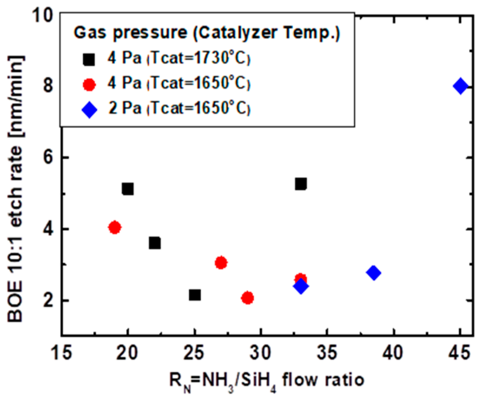
The deposition rate and refractive index of SiNx films obtained under different process conditions are plotted in Figure 2a,b, respectively. The deposition rate for the gas pressure of 2 Pa is <0.4 Å/s, which takes a significant period to deposit conventional passivation layers whose thicknesses are typically at least tens of nanometers. The sample with a refractive index of 1.9 was considered as a reference sample. The wet etch rate is a simple indicator to evaluate the dielectric film quality. It was reported that the wet etch rate had a strong function of the hydrogen content that is known to degrade the film quality and stability characteristics [14,15,16]. The wet etching tests were carried out at room temperature using a 10:1 buffered oxide etchant (BOE), and the results are plotted in Figure 3. The film with a refractive index of 2.12 exhibited the lowest wet etch rate of 2 nm/min, whereas the reference film exhibited a wet etch rate of 7.1 nm/min.
For a detailed analysis of the films, four different films were selected, which had a refractive index of 1.90, 2.02, 2.12, and 2.43. The surface roughness and breakdown field of each sample were measured. Moreover, X-ray reflection (XRR) and Fourier-transform infrared (FT-IR) measurements were carried out to evaluate the density and hydrogen content of the films, respectively. Table 2 presents the surface roughness, breakdown field, film density, and hydrogen content of the selected films.
The surface roughness of the film with a refractive index of 2.12 was 0.28 nm, which is significantly lower than that of the reference film with a refractive index of 1.90. The film density of the sample with a refractive index of 2.12 was 2.7 g/cm3, which was the highest among the samples investigated. The high film density suggested that the film contained relatively less impurities. Indeed, the film density had the same tendency as the BOE wet etch rate.
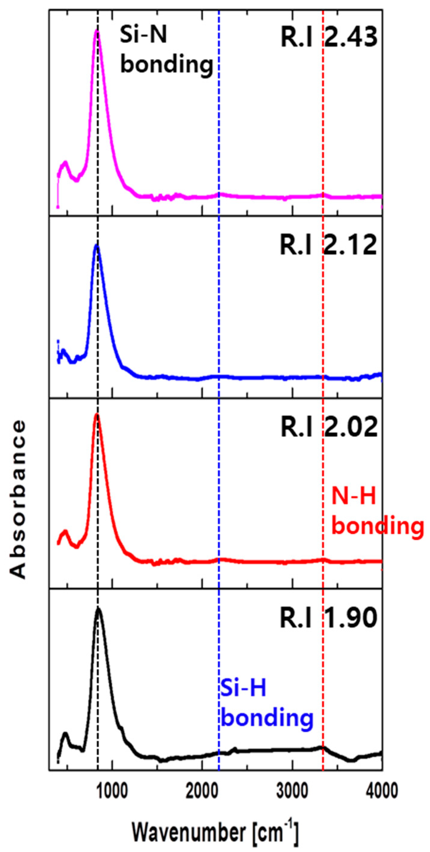
Figure 4 shows the FT-IR absorption spectra of the selected films. The IR absorption spectra exhibited peaks at 830 cm−1, 2100 cm−1, and 3350 cm−1, corresponding to Si–N, Si–H, and N–H bonding, respectively [15]. The relative hydrogen concentration in atomic % was determined from the bond concentrations calculated from the FT-IR spectra. The hydrogen content of the film with a refractive index of 2.12 was 6%, which was significantly lower than that of the reference sample.
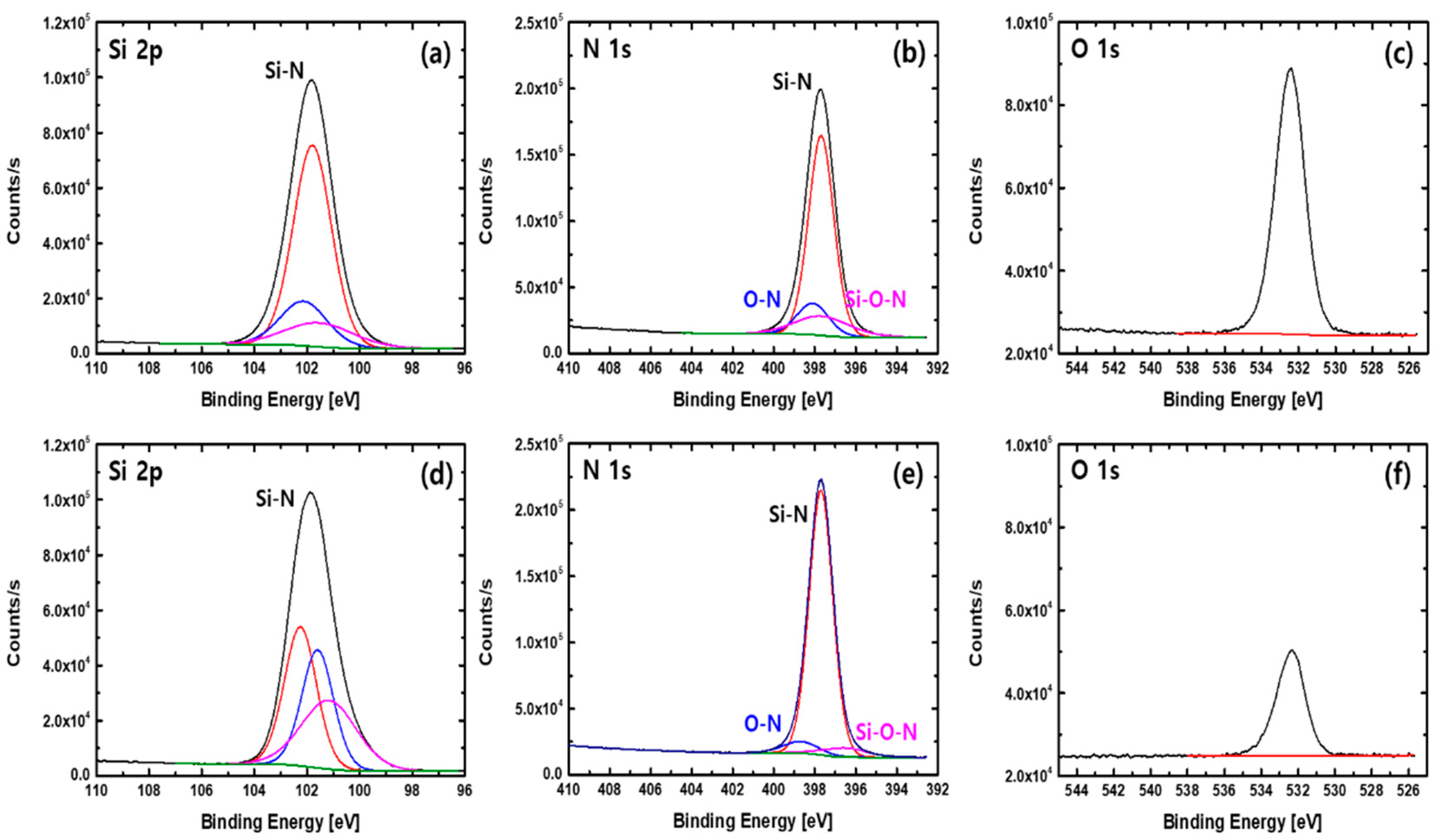
In order to investigate the chemical composition of the film, X-ray photoelectron spectroscopy (XPS) analysis was carried on the reference film with a refractive index of 1.90 and a film with a refractive index of 2.12. Spectra of the core levels of Si, N, O, and C were collected and analyzed. Figure 5 shows the chemical compositions of the two films. Si 2p and N 1s are the main species in the SiNx films. From Figure 5f, the oxygen impurity concentration for the film with a refractive index of 2.12 was significantly lower than that for the reference film. The oxygen impurities were reduced from 11.5% to 4.7%. Furthermore, the carbon impurity concentration decreased from 1.5% to 0.9%. As indicated in Figure 5e, the N 1s peak for the film with a refractive index of 2.12 is ascribed to the Si–N, N–O, and Si–O–N bonds whose respective binding energies are 397.7 eV, 398.1 eV, and 397.6 eV. The atomic concentrations of Si–N, N–O, and Si–O bonds in the film with a refractive index of 2.12 were 88.63%, 5.8%, and 5.58% [17], whereas those for the reference film were 70.9%, 14.13%, and 14.97%, respectively. The O 1s and Si 2p peaks were in agreement with the peaks reported in References [17,18,19]. The total amounts of Si and N peak intensity of the optimized film were 46.74% and 47.51%, respectively, while those of the reference film were 41.99% and 45%, respectively.
Based on film analysis, the deposition conditions for the film with a refractive index of 2.12 were determined to be optimum; a NH3/SiH4 flow ratio of 29, a gas pressure of 4 Pa, and a chuck temperature of 250 °C with a catalyzer temperature of 1650 °C. The deposition rate of the optimized SiNx passivation process was ~0.6 Å/s with a thickness variation of 1.16% across a 4-inch wafer. The optimized film exhibited a film density of 2.7 g/cm3, a BOE etch rate of ~2 nm/min, and a breakdown field of 8.2 MV/cm.
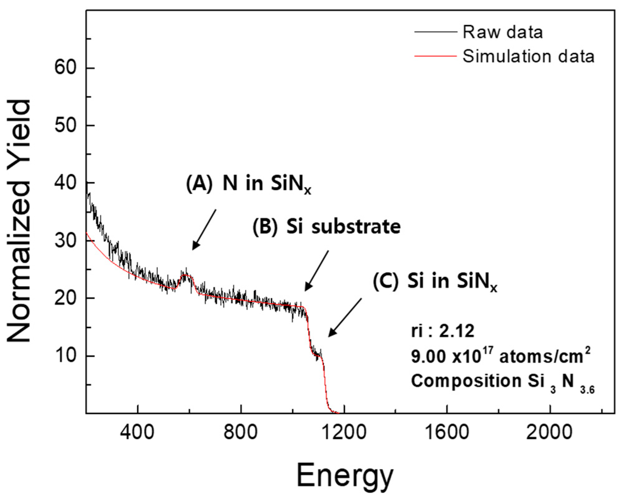
As shown in Figure 6, a Rutherford Backscattering Spectrometry (RBS) analysis was carried out to investigate the stoichiometry of the film with a refractive index of 2.12 where a 115 nm thick film was used to obtain reliable analysis data. The stoichiometry of SiNx film defined by x = [N]/[Si] was 1.2, which was lower than the standard stoichiometric Si3N4 film of 1.33 [20,21]. The smaller x value indicates a Si-rich thin film compared to the stoichiometric Si3N4 film, which is associated with positive charges in the film.
2.2. Device Fabrication
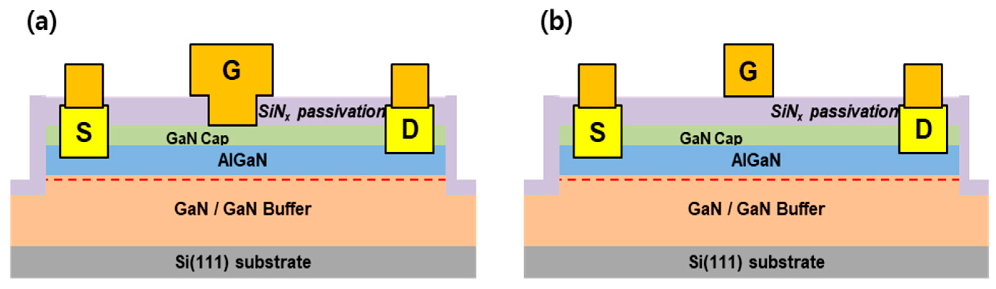
The epitaxial layers consisted of a 2 nm GaN capping layer, 20 nm AlGaN barrier layer, 300 nm undoped GaN layer, and 1.6 μm GaN buffer layer grown on a Si (111) substrate. After solvent cleaning, 40 nm thick SiNx film was deposited using a Cat-CVD system to protect the GaN surface during high-temperature ohmic annealing. Ohmic contacts with a source-to-drain distance of 6 μm were formed by low-damage recess etching using a BCl3/Cl2-based plasma process prior to Si/Ti/Al/Mo/Au (=5/20/80/35/50 nm) metallization [22]. The ohmic contacts were annealed by a rapid thermal annealing process at 800 °C for 1 min in N2 ambient. Mesa isolation was then performed by a BCl3/Cl2 plasma etching process with a relatively higher plasma power. The SiNx protection layer was removed by an SF6-based low-damage plasma etching process in order to eliminate any surface damage during ohmic annealing. A new SiNx film with a thickness of 30 nm was deposited again as a passivation layer using the same Cat-CVD system. SiNx films with three different refractive index values (1.9, 2.12, and 2.43) were deposited for comparison. The deposition conditions for each refractive index value were identical to those shown in Table 1. Post-deposition annealing was conducted at 500 °C for 10 min in N2 ambient. Finally, a gate foot length of 1.5 μm was defined by photolithography, under which the SiNx layer was etched by an SF6 plasma etching process. A Ni/Mo/Au (=40/15/400 nm) metal stack was used for the Schottky gate contact with a gate overhang length of 0.5 μm toward the source and drain contacts. Metal-insulator-semiconductor (MIS) gate devices with the same gate process on the SiNx passivation layer were fabricated without etching for analyzing the interface quality. The cross-sectional schematics of the Schottky and MIS gate HEMTs are presented in Figure 7.
3. Results
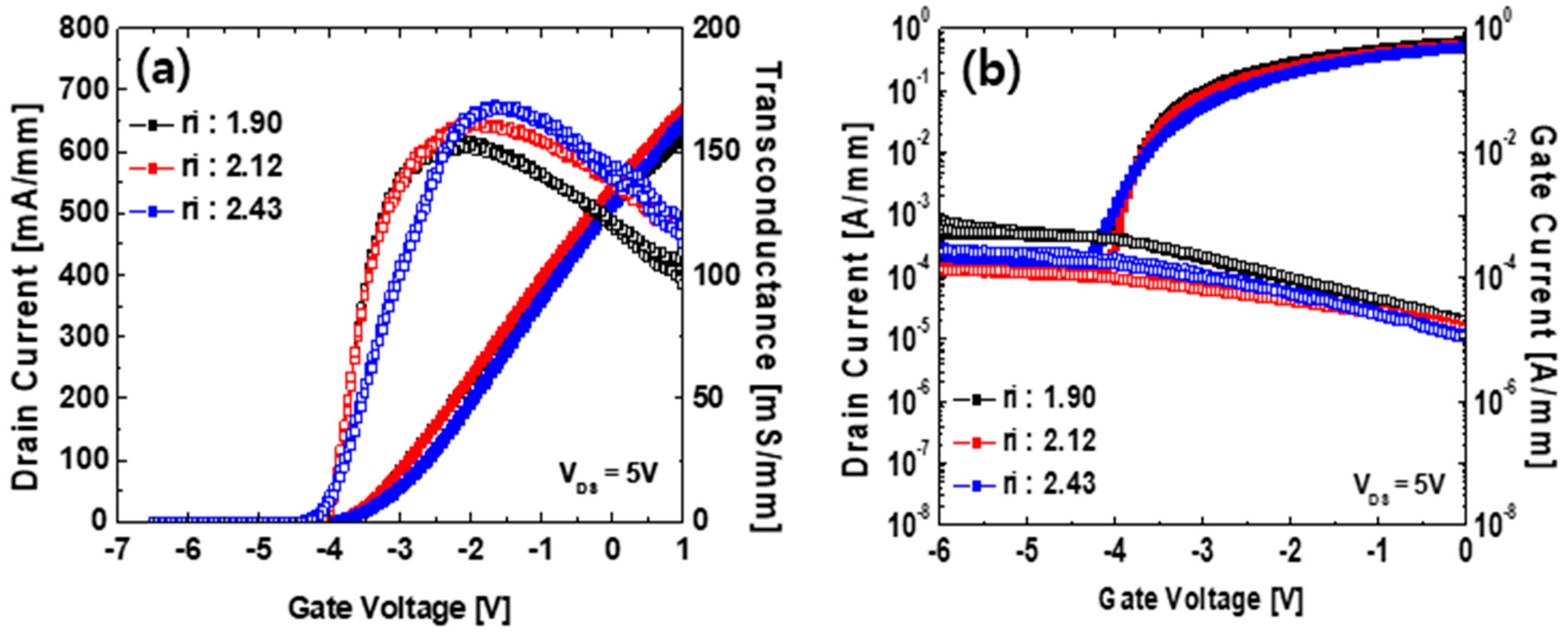
It was observed that the maximum drain current and transconductance were enhanced along with the off-state drain current reduction as the refractive index of the passivation layer increased. As revealed in Figure 8, the maximum drain current density and transconductance of the device for the optimized passivation process condition with a refractive index of 2.12 are 670 mA/mm and 162 mS/mm, respectively.
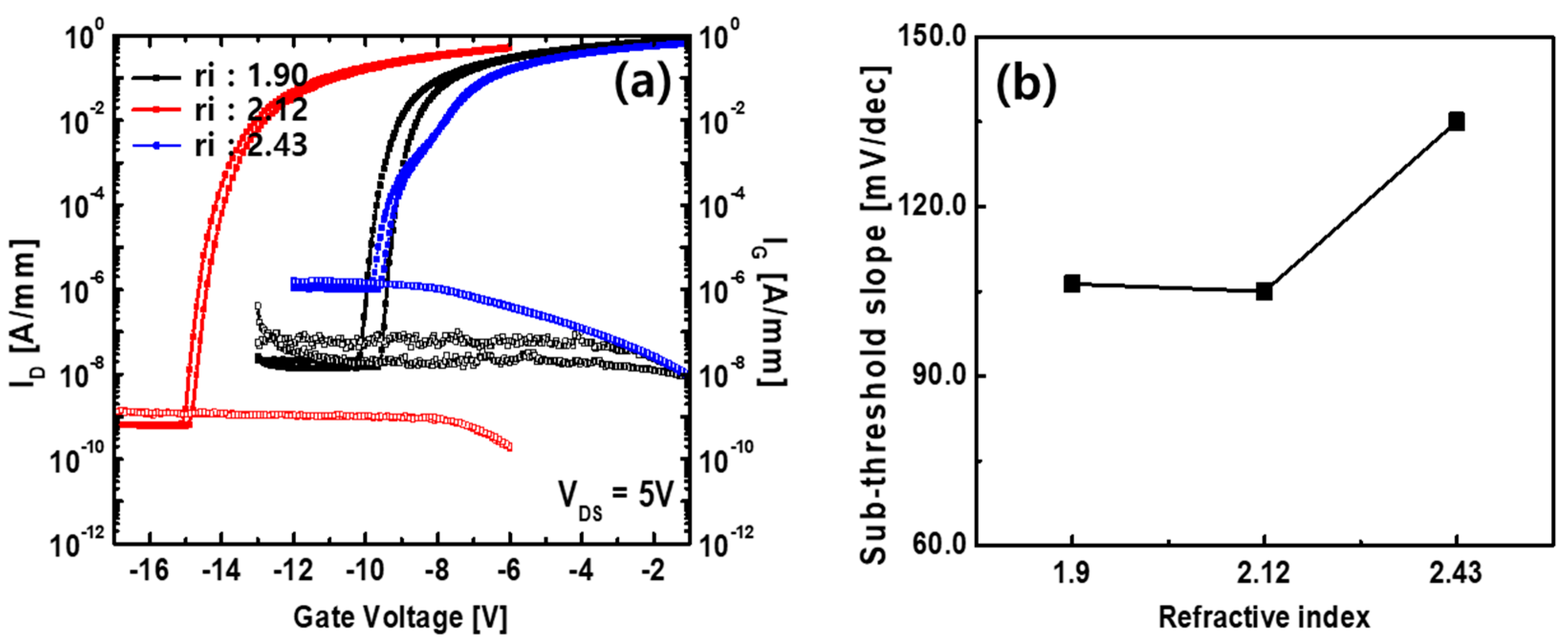
The transfer and sub-threshold slope characteristics of MIS AlGaN/GaN-on-Si HEMTs with 30 nm SiNx layers with different refractive indices are compared in Figure 9. It should be noted that the device with a refractive index of 2.12 exhibited significant negative shift in threshold voltage with the lowest leakage current density, which is 1.3 × 10⁻⁹ A/mm, along with a small sub-threshold slope of 105 mV/dec. The negative shift in threshold voltage can be explained by positive charges in the SiNx film in conjunction with the low H content. As compared in Table 2, the film with a refractive index of 2.12 had the lowest H content and the films with refractive indices of 1.90 and 2.43 had relatively higher H contents. The interface fixed charges and bulk charges of the film with a refractive index of 2.12 are discussed later with capacitance-voltage (C-V) measurements.
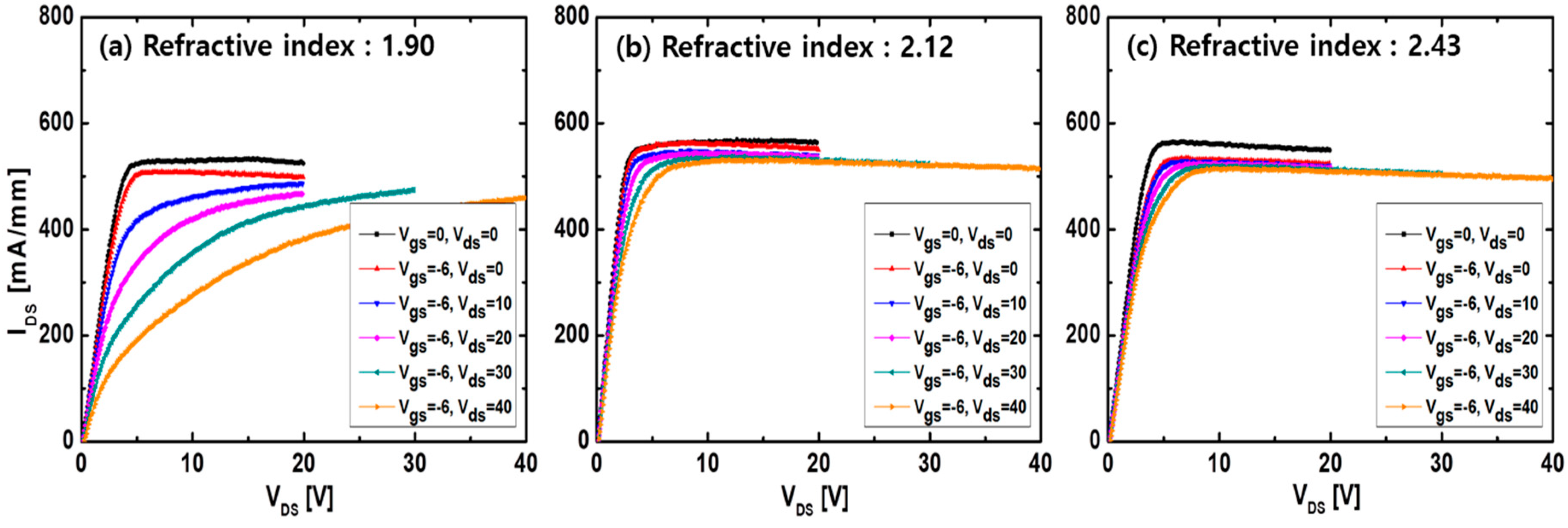
In order to investigate the current collapse phenomenon, the devices were measured under pulse mode operation with a pulse width of 200 ns and a pulse period of 1 ms where the quiescent bias conditions were varied by VGSQ = 0/−6 V and VDSQ = 0/10/20/30/40 V. We observed that the pulsed current-voltage characteristics were significantly improved by employing the optimized passivation process. The current collapse phenomenon was defined by the reduction of drain current density from a drain voltage of 5 V with VDSQ = 0 V to a drain voltage of 10 V with VDSQ = 40 V [8,9]. The current collapse reduction of the Schottky gate HEMT with the passivation film with a refractive index of 2.12 exhibited superior characteristics to others in Figure 10. The current collapse reduction was only 6.5%.
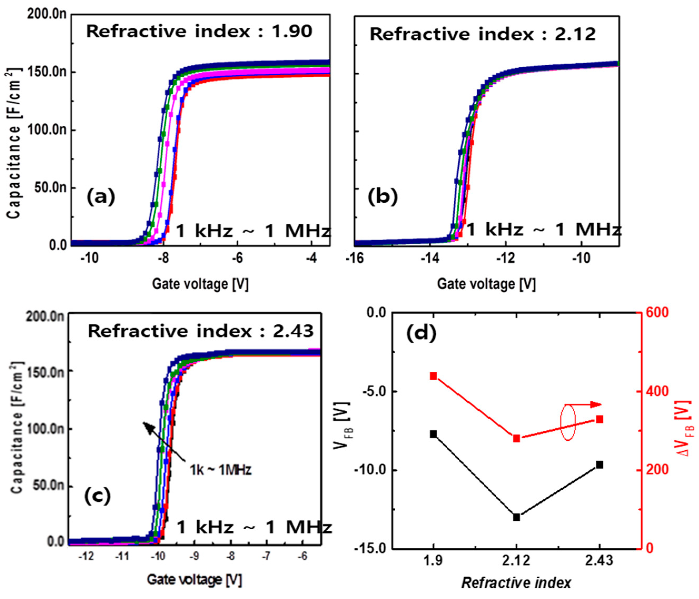
Trapping effects at the surface states are responsible for the current collapse phenomenon of AlGaN/GaN HEMTs. In order to suppress the electron trapping effects, the passivation film must have positive charges to attract the trapped electrons [23,24,25,26,27]. The net charges of the SiNx film can be modified under the deposition conditions that alter the stoichiometry of SiNx. To investigate the fixed charges of the passivation films, the frequency-dependent C-V characteristics of MIS gate devices were measured from 1 kHz to 1 MHz, from which the flat-band voltage and hysteresis characteristics could be determined. The MIS gate device had a circular MIS gate with a diameter of 100 μm, which was surrounded by an ohmic electrode. In Figure 10a,c, the threshold voltage is negatively shifted with increasing refractive index [24,28,29], which indicates that a high-refractive-index film has more positive fixed charges in the MIS gate than the films with lower refractive indices. In comparison with the reference film with a refractive index of 1.90, the flat-band voltage of the device with the film having a refractive index of 2.12 was negatively shifted from −7.7 V to −13 V with smaller flat band voltage hysteresis (Figure 11d). The flat-band voltage hysteresis was reduced from 440 mV for a refractive index of 1.90 to 280 mV for a refractive index of 2.12.
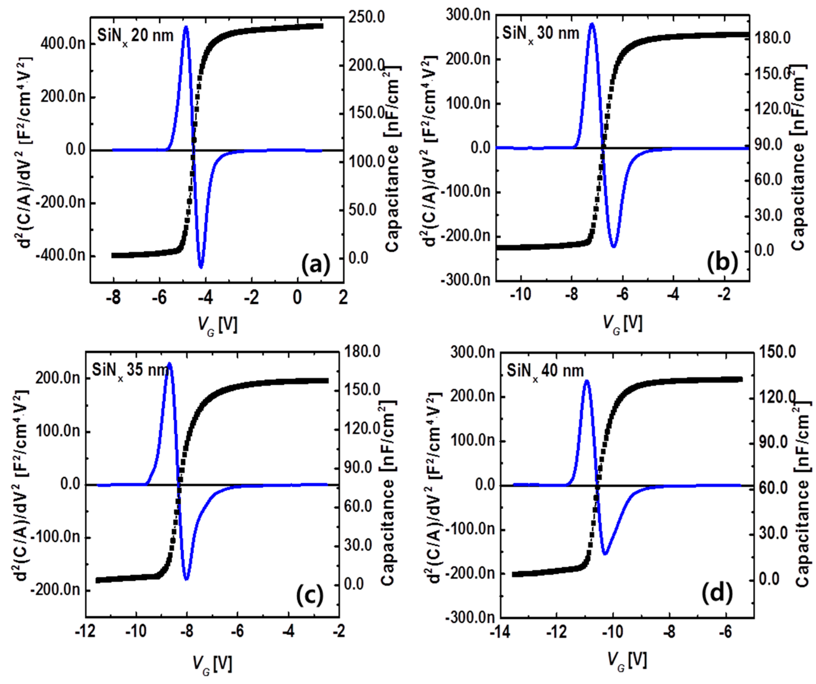
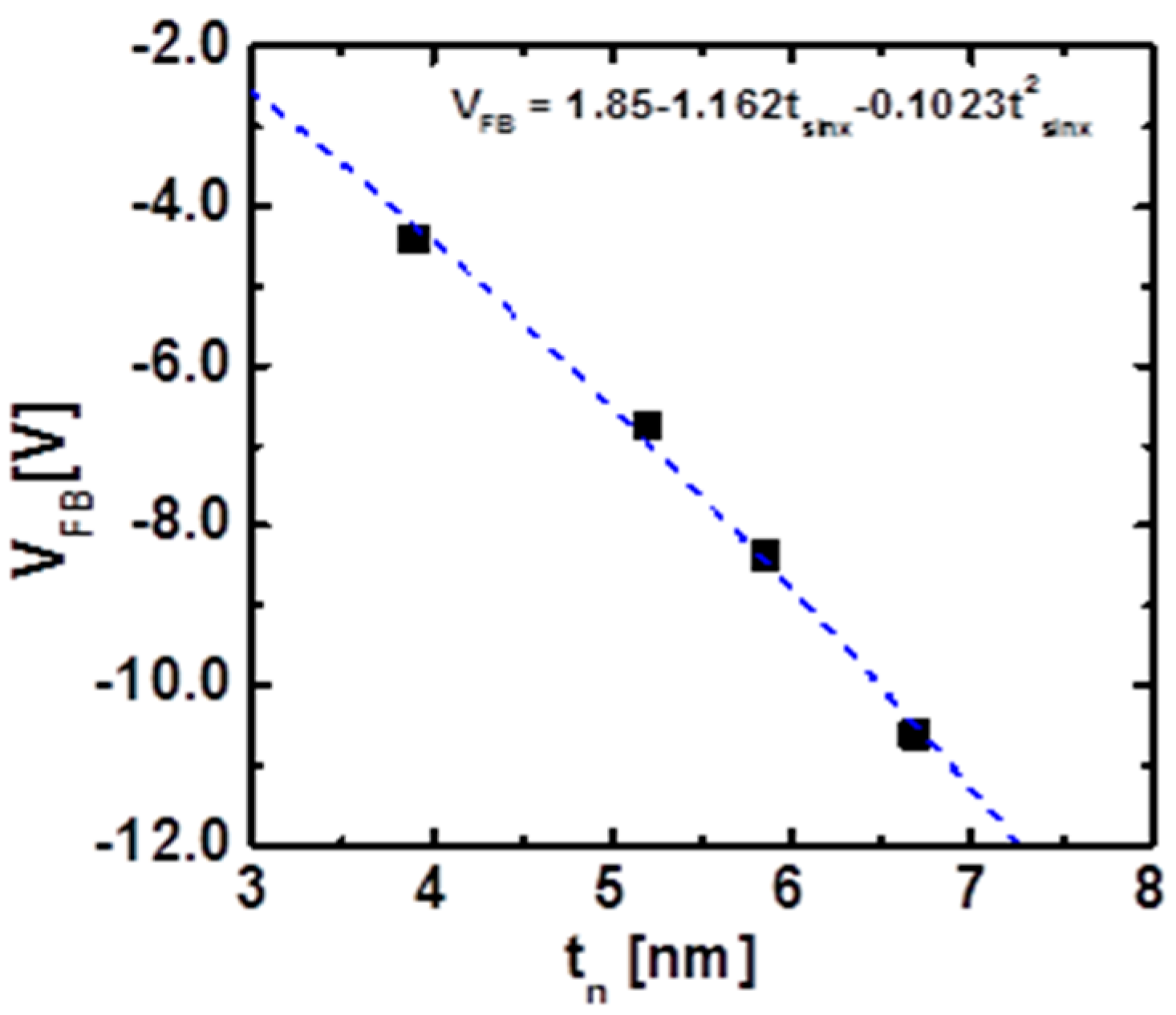
In order to extract the fixed charge density of the optimized film, four samples were prepared with different SiNx thicknesses: 20, 30, 35, and 40 nm. It should be noted that the AlGaN barrier layer used for the experiments was 9 nm, which was relatively thinner than that used for device fabrication. The density of fixed charges at the SiNx on the surface was extracted by Vth-thickness dependency. A second derivative method [29] was used to obtain a flat-band voltage from the C-V characteristics as a function of SiNx thickness. The flat-band voltage was plotted against the normalized total cap thickness (tn = tn (SiNx) + tn (AlGaN) = tsinx/εsinx + tAlGaN/εAlGaN) [30]. The flat-band voltages extracted for SiNx thicknesses of 20, 30, 35, and 40 nm were −4.4, −6.8, −8.4, and −10.6 V, respectively. Figure 12 and Figure 13 present the extracted flat-band voltages of the AlGaN/GaN MIS FETs with SiNx dielectric films as a function of film thickness. The interface fixed charge density and bulk charge density can be extracted by [31]
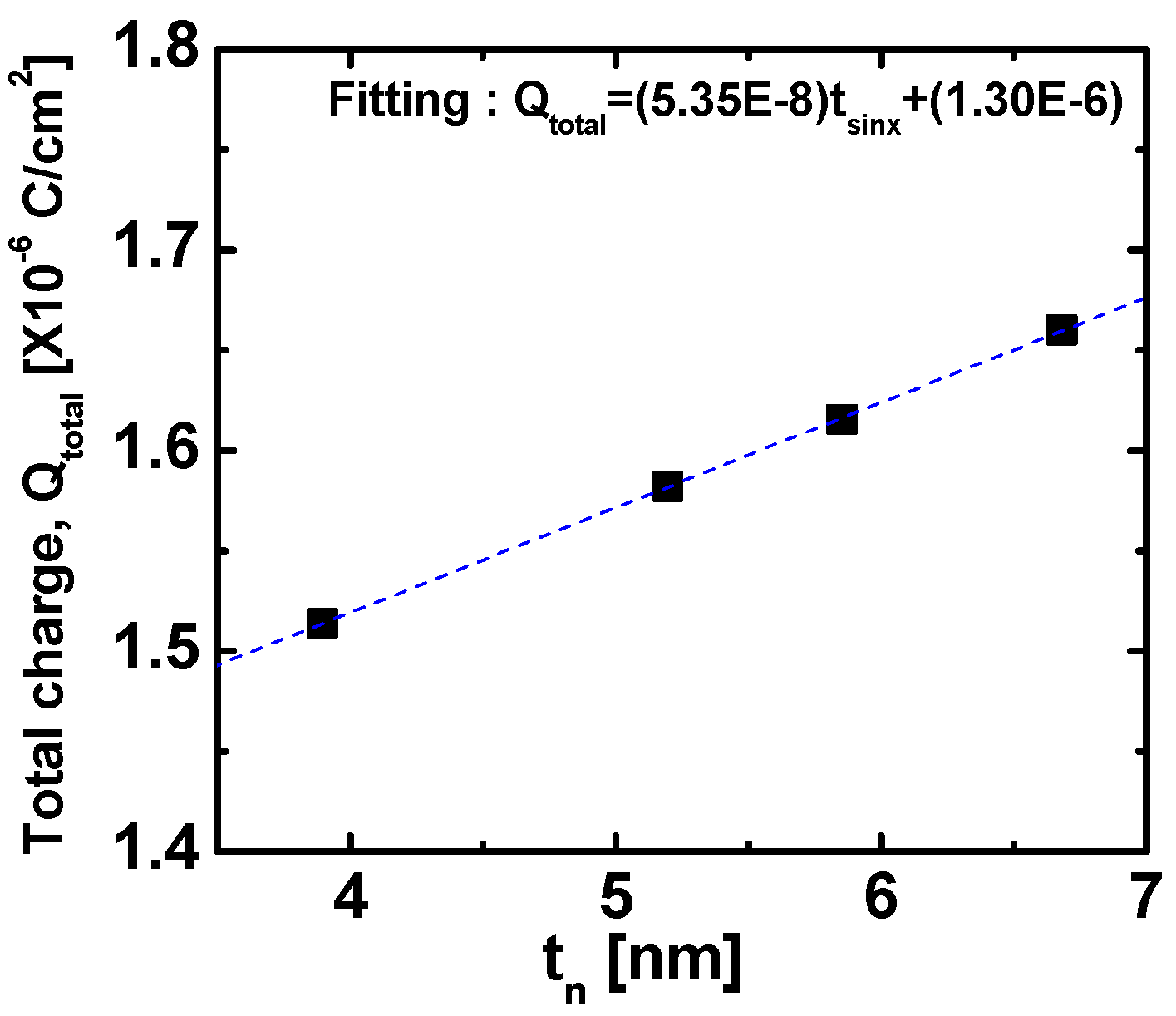
where VFB is the flat-band voltage, WMS is the work function difference between the metal and semiconductor, Qint is the total charge, Qbulk is the bulk charge, and tox is the dielectric thickness. The total charge densities as a function of the SiNx film thickness are indicated in Figure 14.
Assuming that the AlGaN polarization charge for an Al mole fraction of 0.2 and a barrier thickness of 9 nm was 1.5 × 1012 cm−2 [32], the extracted interface fixed charge density and the bulk charge density were estimated to be 6.63 × 1012 cm−2 and 3.3 × 1018 cm−3, respectively. It is suggested that the large amounts of positive interface and bulk charges of the SiNx passivation film were responsible for the significant negative shift of Vth of the MIS HEMT as shown in Figure 9. The positive charges in the MIS gate acted as a virtual gate that required more negative voltage to deplete the 2DEG channel.
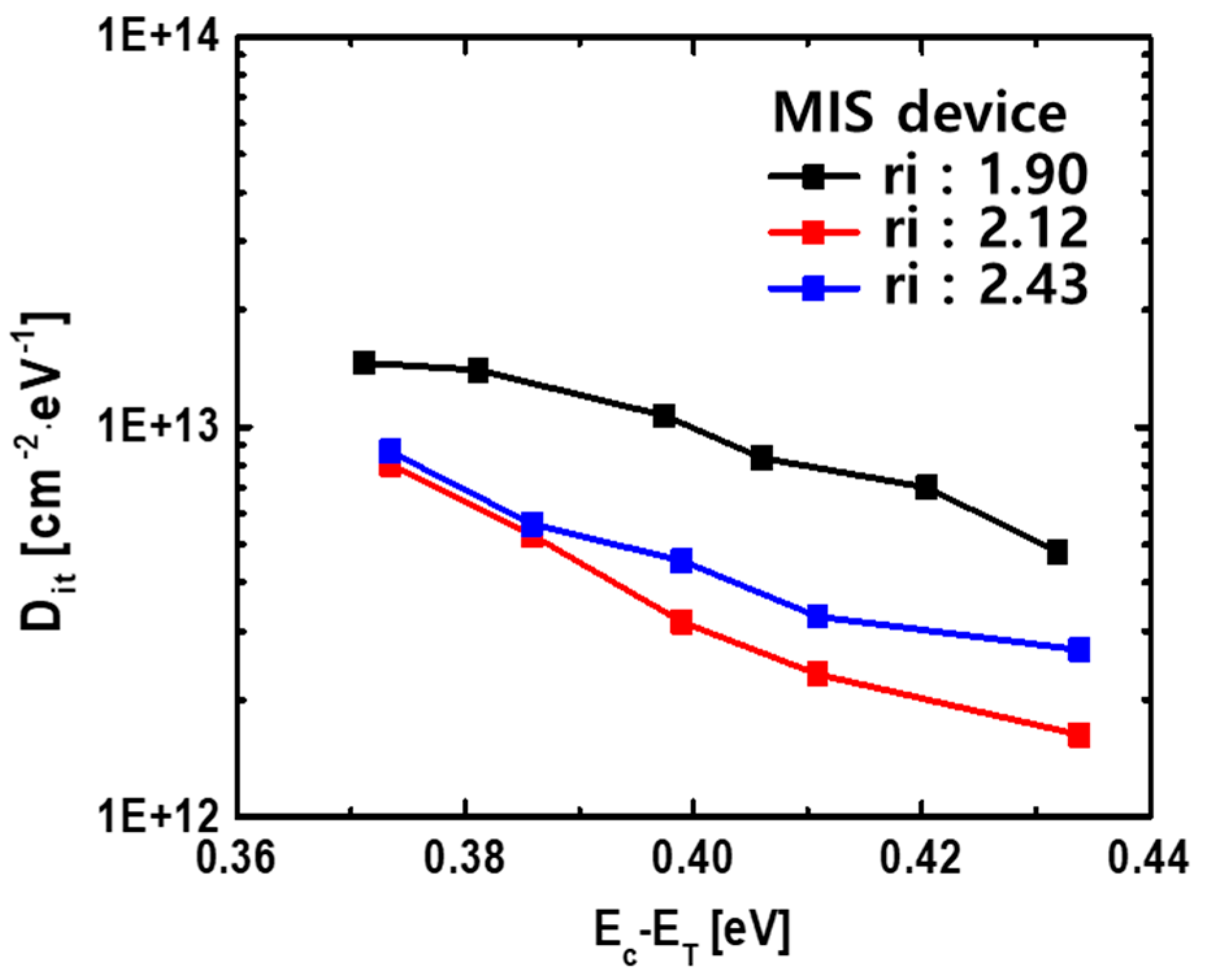
The interface trap density (Dit) for MIS gates was investigated using a conductance method [33]. The extracted Dit characteristics are plotted in Figure 15. The lowest Dit level was achieved by a refractive index of 2.12, which was 2 × 1012 cm−2 eV−1 at a trap energy level of 0.43 eV. The low Dit level can further explain the improved current collapse phenomenon observed in the Schottky device. The current collapse characteristics observed in this work are compared with those reported in previous studies [33,34,35,36,37,38] in Table 3. We suggest that the Cat-CVD SiNx passivation process developed in this work is very promising for suppressing the current collapse phenomenon of GaN devices.
4. Conclusions
We have developed a high-quality SiNx film deposition process using a Cat-CVD system for the passivation layer of AlGaN/GaN HEMTs. A Cat-CVD SiNx dielectric layer has been optimized to reduce the trapping phenomenon originating from the surface states. Modification of the SiNx film stoichiometry can result in positive net charges that can effectively suppress the trapping phenomenon. The optimized passivation process conditions were a NH3/SiH4 gas flow ratio of 29, gas pressure of 4 Pa, and chuck temperature of 250 °C with a catalyzer temperature of 1650 °C, which resulted in a refractive index of 2.1. The device fabricated under the optimized passivation process conditions exhibited excellent electrical characteristics. The high film density and low interface trap density of the optimized passivation film were responsible for the improved current–voltage characteristics and caused the suppression of the current collapse phenomenon. Therefore, the Cat-CVD SiNx film is a promising passivation layer for AlGaN/GaN HEMTs.
Author Contributions
Conceptualization, M.-J.K., H.-Y.C. and K.-S.S.; Data curation, M.-J.K. and K.-S.S.; Formal analysis, M.-J.K.; Funding acquisition, H.-Y.C. and K.-S.S.; Investigation, M.-J.K. and H.-S.K.; Methodology, M.-J.K. and H.-S.K.; Supervision, H.-Y.C. and K.-S.S.; Validation, M.-J.K. and H.-S.K.; Visualization, M.-J.K.; Writing—original draft, M.-J.K.; Writing—review & editing, H.-Y.C. and K.-S.S. All authors have read and agreed to the published version of the manuscript.
Funding
This work was supported by BK21 plus Project in 2019, Ministry of Trade, Industry and Energy (10067636), Basic Science Research Programs (2015R1A6A1A03031833 and 2019R1A2C1008894), and Civil-Military Technology Cooperation Program (No. 17-CM-MA-03).
Acknowledgments
Myoung-Jin Kang currently works at the future technology R&D center, SK Hynix Co. Ltd., KOREA.
Conflicts of Interest
The authors declare no conflict of interest.
References
- Mishra, U.K.; Parikh, P.; Wu, Y.-F. AlGaN/GaN HEMTs-an overview of device operation and applications. Proc. IEEE 2002, 90, 1022–1031. [Google Scholar] [CrossRef] [Green Version]
- Kang, M.J.; Lee, M.S.; Choi, G.H.; Hwang, I.H.; Cha, H.Y.; Seo, K.S. High-performance normally off AlGaN/GaN-on-Si HEMTs with partially recessed SiNx MIS structure. Phys. Status Solidi A 2017, 214, 1600726. [Google Scholar] [CrossRef]
- Joh, J.W.; Tipirneni, N.; Pendharkar, S.; Krishnan, S. Current collapse in GaN heterojunction field effect transistors for hihg-voltage switching applications. In Proceedings of the IEEE International Reliability Physics Symposium, Waikolia, HI, USA, 1–5 June 2014. [Google Scholar]
- Javorka, P.; Bernat, J.; Fox, A.; Marso, M.; Lüth, H.; Kordoš, P. Influence of SiO2 and Si3N4 passivation on AlGaN/GaN/Si HEMT performance. Electron. Lett. 2003, 39, 1155–1157. [Google Scholar] [CrossRef]
- Xu, D.; Chu, K.; Diaz, J.; Zhu, W.; Roy, R.; Pleasant, L.M.; Nichols, K.; Chao, P.-C.; Xu, M.; Peide, D.Y. 0.2 um AlGaN/GaN high electron mobility transistors with atomic layer deposition Al2O3 passivation. IEEE Electron. Device Lett. 2013, 36, 744–746. [Google Scholar] [CrossRef]
- Huang, S.; Jiang, Q.; Yang, S.; Zhou, C.; Chen, K.J. Effective passivation of AlGaN/GaN HEMTs by ALD-grown AlN thin film. IEEE Electron. Device Lett. 2012, 33, 516–518. [Google Scholar] [CrossRef]
- Arulkumaran, S.; Egawa, T.; Ishikawa, H.; Jimbo, T.; Sano, Y. Surface passivation effects on AlGaN/GaN high-electron-mobility transistors with SiO2, Si3N4, and silicon oxynitride. Appl. Phys. Lett. 2004, 84, 613–615. [Google Scholar] [CrossRef]
- Ling, Y.; Gui-Zhou, H.; Yue, H.; Xiao-Hua, M.; Si, Q.; Li-Yuan, Y.; Shou-Gao, J. Electric-stress reliability and current collapse of different thickness SiNx passivated AlGaN/GaN high electron mobility transistors. Chin. Phys. B 2010, 19, 047301. [Google Scholar] [CrossRef]
- Wang, X.; Huang, S.; Zheng, Y.; Wei, K.; Chen, X.; Liu, G.; Yuan, T.; Luo, W.; Pang, L.; Jiang, H. Robust SiNx/AlGaN interface in GaN HEMTs passivated by thick LPCVD-grown SiNx layer. IEEE Electron. Device Lett. 2015, 36, 666–668. [Google Scholar] [CrossRef]
- Okada, S.; Matsumura, H. Improved properties of silicon nitride films prepared by the catalytic chemical vapor deposition method. Jpn. J. Appl. Phys. 1997, 36, 7035. [Google Scholar] [CrossRef]
- Higashiwaki, M.; Mimura, T.; Matsui, T. AlN/GaN insulated-gate HFETs using cat-CVD SiN. IEEE Electron. Device Lett. 2006, 27, 719–721. [Google Scholar] [CrossRef]
- Matsumura, H. Formation of silicon-based thin films prepared by catalytic chemical vapor deposition (Cat-CVD) method. Jpn. J. Appl. Phys. 1998, 37, 3175. [Google Scholar] [CrossRef]
- Matsumura, H.; Umemoto, H.; Masuda, A. Cat-CVD (hot-wire CVD): How different from PECVD in preparing amorphous silicon. J. Non-Cryst. Solids 2004, 338, 19–26. [Google Scholar] [CrossRef]
- Verlaan, V.; Verkerk, A.; Arnoldbik, W.; van der Werf, C.; Bakker, R.; Houweling, Z.; Romijn, I.; Borsa, D.; Weeber, A.; Luxembourg, S. The effect of composition on the bond structure and refractive index of silicon nitride deposited by HWCVD and PECVD. Thin Solid Films 2009, 517, 3499–3502. [Google Scholar] [CrossRef] [Green Version]
- Masuda, A.; Totsuka, M.; Oku, T.; Hattori, R.; Matsumura, H. Highly moisture-resistive silicon nitride films prepared by catalytic chemical vapor deposition and application to gallium arsenide field-effect transistors. J. Vac. 2004, 74, 525–529. [Google Scholar] [CrossRef]
- Masuda, A.; Izumi, A.; Umemoto, H.; Matsumura, H. What is the difference between catalytic CVD and plasma-enhanced CVD? Gas-phase kinetics and film properties. J. Vac. 2002, 66, 293–297. [Google Scholar] [CrossRef]
- Kim, S.; Chang, Y.-F.; Park, B.-G. Understanding rectifying and nonlinear bipolar resistive switching characteristics in Ni/SiNx/p-Si memory devices. RCS Adv. 2017, 7, 17882. [Google Scholar] [CrossRef] [Green Version]
- Ma, H.-P.; Lu, H.-L.; Yang, J.-H.; Li, X.-X.; Wang, T.; Huang, W.; Yuan, G.-J.; Kamarov, F.F.; Zhang, D.W. Measurements of Microstructural, Chemical, Optical, and Electrical Properties of Silicon-Oxygen-Nitrogen Films Prepared by Plasma-Enhanced Atomic Layer Deposition. Nanomaterials 2018, 8, 1008. [Google Scholar] [CrossRef] [Green Version]
- Kitao, A.; Imakita, K.; Kawamura, I.; Fujii, M. An investigation into second harmonic generation by Si-rich SiNx thin films deposited by RF sputtering over a wide range of Si concentrations. J. Phys. D Appl. Phys. 2014, 47, 215101. [Google Scholar] [CrossRef]
- Meziani, S.; Moussi, A.; Mahiou, L.; Outemzabet, R. Compositional analysis of silicon oxide/silicon nitride thin films. Mater. Sci. Pol. 2016, 34, 315–321. [Google Scholar] [CrossRef] [Green Version]
- Tiour, F.; Benyahia, B.; Brihi, N.; Sari, A.; Mahmoudi, B.; Manseri, A.; Guenda, A. Opto-structural properties of Si-rich SiNx with diferent stoichiometry. Appl. Phys. A 2020, 126, 59. [Google Scholar] [CrossRef]
- Kang, M.J.; Eom, S.K.; Kim, H.S.; Lee, C.H.; Cha, H.Y.; Seo, K.S. Normally-off recessed-gate AlGaN/GaN MOS-HFETs with plasma enhanced atomic layer deposited AlOxNy gate insulator. Semicond. Sci. Technol. 2019, 34, 055018. [Google Scholar] [CrossRef]
- Warren, W.L.; Kanicki, J.; Robertson, J.; Lenahan, P.M. Energy level of the nitrogen dangling bond in amorphous silicon nitride. Appl. Phys. Lett. 1991, 59, 1699–1701. [Google Scholar] [CrossRef]
- Waller, W.M.; Gajda, M.; Pandey, S.; Donkers, J.J.; Calton, D.; Croon, J.; Karboyan, S.; Sonsky, J.; Uren, M.J.; Kuball, M. Impact of Silicon Nitride Stoichiometry on the Effectiveness of AlGaN/GaN HEMT Field Plates. IEEE Trans. Elec. Devices 2017, 64, 1197–1202. [Google Scholar] [CrossRef] [Green Version]
- Liu, S.; Huang, C.; Chang, C.; Lin, Y.; Chen, B.; Tsai, S.; Yeop, B.; Dee, C.; Chang, E.Y. Effective Passivation with High-Density Positive Fixed Charges for GaN MIS-HEMTs. J. Electr. Devices Soc. 2017, 5, 170–174. [Google Scholar] [CrossRef]
- Thi, T.C.; Koyama, K.; Ohdaira, K.E.; Matsumura, H. Effect of hydrogen on passivation quality of SiNx/Si-rich SiNx stacked layers deposited by catalytic chemical vapor deposition on c-Si wafers. Thin Solid Films 2015, 575, 60–63. [Google Scholar] [CrossRef] [Green Version]
- Waller, W.M.; Gajda, M.; Pandey, S.; Donkers, J.J.T.M.; Calton, D.; Croon, J.; Sonsky, J.; Uren, M.J.; Kuball, M. Control of Buffer-Induced Current Collapse in AlGaN/GaN HEMTs Using SiNx Deposition. IEEE Trans. Elec. Devices 2017, 64, 4044–4049. [Google Scholar] [CrossRef] [Green Version]
- Huang, T.; Jiang, H.; Bergsten, J.; Lau, K.M.; Rorsman, N. Enhanced gate stack stability in GaN transistors with gate dielectric of bilayer SiNx by low pressure chemical vapor deposition. Appl. Phys. Lett. 2018, 113, 232102. [Google Scholar] [CrossRef] [Green Version]
- Winter, R.; Ahn, J.; McIntyre, P.C.; Eizenberg, M. New method for determining flat-band voltage in high mobility semiconductors. J. Vac. Sci. Technol. B Nanotechnol. Microelectron. Mater. Process. Meas. Phenom. 2013, 31, 030604. [Google Scholar] [CrossRef] [Green Version]
- Capriotti, M.; Alexewicz, A.; Fleury, C.; Gavagnin, M.; Bethge, O.; Visalli, D.; Derluyn, J.; Wanzenböck, H.; Bertagnolli, E.; Pogany, D. Fixed interface charges between AlGaN barrier and gate stack composed of in situ grown SiN and Al2O3 in AlGaN/GaN high electron mobility transistors with normally off capability. Appl. Phys. Lett. 2014, 104, 113502. [Google Scholar] [CrossRef]
- Kim, H.-S.; Eom, S.-K.; Seo, K.-S.; Kim, H.; Cha, H.-Y. Time-dependent dielectric breakdown of recessed AlGaN/GaN-on-Si MOS-HFETs with PECVD SiO2 gate oxide. Vacuum 2018, 155, 428–433. [Google Scholar] [CrossRef]
- Ambacher, O.; Smart, J.; Shealy, J.; Weimann, N.; Chu, K.; Murphy, M.; Schaff, W.; Eastman, L.; Dimitrov, R.; Wittmer, L. Two-dimensional electron gases induced by spontaneous and piezoelectric polarization charges in N-and Ga-face AlGaN/GaN heterostructures. J. Appl. Phys. 1999, 85, 3222–3233. [Google Scholar] [CrossRef] [Green Version]
- Schroder, D.K. Semiconductor Material and Device Characterization; John Wiley & Sons: Hoboken, NJ, USA, 2015. [Google Scholar]
- Geng, K.; Chen, D.; Zhou, Q.; Wang, H. AlGaN/GaN MIS-HEMT with PECVD SiNx, SiON, SiO2 as gate dielectric and passivation layer. Electronics 2018, 7, 416. [Google Scholar] [CrossRef] [Green Version]
- Kim, D.; Jeong, J.; Eom, S.; Lee, J.; Seo, K. Electrical degradation on DC and RF characteristics of short channel AlGaN/GaN-on-Si hemt with highly doped carbon buffer. J. Korean Phys. Soc. 2017, 71, 697–700. [Google Scholar] [CrossRef]
- Tzou, A.; Chu, K.; Lin, I.; Streng, E.; Fang, Y.; Wu, X.; Wu, B.; Shen, C.; Shieh, J.; Yeh, W.; et al. AlN surface passivation of GaN-based high electron mobility transistors by plasma-enhanced atomic layer deposition. Nanoscale Res. Lett. 2017, 12, 315. [Google Scholar] [CrossRef] [PubMed] [Green Version]
- Chakroun, A.; Jaouad, A.; Bouchilaoun, M.; Arenas, O.; Soltani, A.; Maher, H. Normally-off AlGaN/GaN MOS-HEMT using ultra-thin Al0.45Ga0.55N barrier layer. Phys. Status Solidi A 2017, 214, 1600836. [Google Scholar] [CrossRef]
- Zhang, S.; Wei, K.; Ma, X.; Hou, B.; Liu, G.; Zhang, Y.; Wang, X.; Zheng, Y.; Huang, S.; Li, Y.; et al. Reduced reverse gate leakage current for GaN HEMTs with 3 nm Al/40 nm SiN passivation layer. Appl. Phys. Lett. 2019, 114, 013503. [Google Scholar] [CrossRef]
Figure 1.
The schematic diagram of Cat-CVD system.

Figure 2.
(a) Deposition rate and (b) refractive index versus NH3/SiH4 flow ratio as a function of gas pressure.
Figure 2.
(a) Deposition rate and (b) refractive index versus NH3/SiH4 flow ratio as a function of gas pressure.

Figure 3.
Buffered oxide etchant (BOE) (10:1) wet etch rate versus gas flow rate as functions of gas pressure.
Figure 3.
Buffered oxide etchant (BOE) (10:1) wet etch rate versus gas flow rate as functions of gas pressure.

Figure 4.
Fourier-transform infrared (FT-IR) absorption spectra as a function of refractive index under various deposition conditions of Cat-CVD SiNx.
Figure 4.
Fourier-transform infrared (FT-IR) absorption spectra as a function of refractive index under various deposition conditions of Cat-CVD SiNx.

Figure 5.
XPS spectra for Cat-CVD SiNx deposited with reference and optimized conditions with refractive index values of 1.90 and 2.12, respectively; (a–c) reference film and (d–f) optimized film.
Figure 5.
XPS spectra for Cat-CVD SiNx deposited with reference and optimized conditions with refractive index values of 1.90 and 2.12, respectively; (a–c) reference film and (d–f) optimized film.

Figure 6.
Rutherford backscattering spectrometry (RBS) spectrum of the optimized SiNx film deposited on Si wafer.
Figure 6.
Rutherford backscattering spectrometry (RBS) spectrum of the optimized SiNx film deposited on Si wafer.

Figure 7.
Cross-sectional schematics of fabricated (a) Schottky and (b) metal-insulator-semiconductor (MIS) gate AlGaN/GaN-on-Si high electron mobility transistors (HEMTs) with SiNx passivation films.
Figure 7.
Cross-sectional schematics of fabricated (a) Schottky and (b) metal-insulator-semiconductor (MIS) gate AlGaN/GaN-on-Si high electron mobility transistors (HEMTs) with SiNx passivation films.

Figure 8.
Transfer characteristics (a) on a linear scale and (b) log scale of the Schottky gate AlGaN/GaN-on-Si HEMTs with 30 nm SiNx passivation layers with different refractive indices.
Figure 8.
Transfer characteristics (a) on a linear scale and (b) log scale of the Schottky gate AlGaN/GaN-on-Si HEMTs with 30 nm SiNx passivation layers with different refractive indices.

Figure 9.
(a) Transfer and (b) sub-threshold slope characteristics of MIS AlGaN/GaN-on-Si HEMTs with 30 nm SiNx layers with different refractive indices. The measurements were carried out at VD = 5 V.
Figure 9.
(a) Transfer and (b) sub-threshold slope characteristics of MIS AlGaN/GaN-on-Si HEMTs with 30 nm SiNx layers with different refractive indices. The measurements were carried out at VD = 5 V.

Figure 10.
Current collapse characteristics of Schottky gate AlGaN/GaN-on-Si HEMTs with 30 nm SiNx passivation layers with different refractive indexes of (a) 1.90, (b) 2.12, and (c) 2.43.
Figure 10.
Current collapse characteristics of Schottky gate AlGaN/GaN-on-Si HEMTs with 30 nm SiNx passivation layers with different refractive indexes of (a) 1.90, (b) 2.12, and (c) 2.43.

Figure 11.
(a–c) Frequency dispersion characteristics from 1 kHz to 1 MHz of a 30 nm SiNx dielectric layer. (d) Flat-band voltage (VFB) and hysteresis (∆VFB) of the MIS gate AlGaN/GaN-on-Si HEMTs for different refractive indices. The inset of (d) is a schematic view of the C-V measurement pattern.
Figure 11.
(a–c) Frequency dispersion characteristics from 1 kHz to 1 MHz of a 30 nm SiNx dielectric layer. (d) Flat-band voltage (VFB) and hysteresis (∆VFB) of the MIS gate AlGaN/GaN-on-Si HEMTs for different refractive indices. The inset of (d) is a schematic view of the C-V measurement pattern.

Figure 12.
Flat-band voltages extracted by the second derivative method from C-V characteristics: (a) 20 nm, (b) 30 nm, (c) 35 nm, and (d) 40 nm SiNx films.
Figure 12.
Flat-band voltages extracted by the second derivative method from C-V characteristics: (a) 20 nm, (b) 30 nm, (c) 35 nm, and (d) 40 nm SiNx films.

Figure 13.
Flat-band voltage versus SiNx film thickness.

Figure 14.
Total charge densities of Cat-CVD SiNx films versus film thickness.

Figure 15.
Interface trap density (Dit) characteristics of MIS gate AlGaN/GaN-on-Si HEMTs with different SiNx films.
Figure 15.
Interface trap density (Dit) characteristics of MIS gate AlGaN/GaN-on-Si HEMTs with different SiNx films.


Table 1.
Catalytic-chemical vapor deposition (Cat-CVD) silicon nitride (SiNx) properties as function of deposition conditions.
Table 1.
Catalytic-chemical vapor deposition (Cat-CVD) silicon nitride (SiNx) properties as function of deposition conditions.
| Chuck Temp [°C] | Wire Temp [°C] | Pressure [Pa] | NH3/SiH4 | Dep Rate [A/s] | R.I. | BOE (10:1) Etch Rate [nm/min] |
|---|---|---|---|---|---|---|
| 400 | 1730 | 4 | 5 | 0.90 | 1.90 | 7.1 |
| 400 | 1730 | 4 | 50 | 0.88 | 1.94 | 4.80 |
| 350 | 1730 | 4 | 50 | 0.86 | 1.96 | 3.72 |
| 250 | 1730 | 4 | 45 | 0.80 | 1.97 | 2.22 |
| 150 | 1730 | 4 | 45 | 0.81 | 1.99 | 3.57 |
| 250 | 1600 | 4 | 19 | 0.56 | 2.83 | - |
| 250 | 1730 | 4 | 20 | 0.77 | 2.31 | 5.14 |
| 250 | 1730 | 4 | 25 | 0.75 | 2.03 | 2.15 |
| 250 | 1730 | 4 | 33 | 0.60 | 1.94 | 5.28 |
| 250 | 1650 | 2 | 50 | 0.30 | 1.90 | 8.02 |
| 250 | 1650 | 2 | 38.5 | 0.36 | 2.00 | 2.77 |
| 250 | 1650 | 2 | 33.3 | 0.38 | 2.12 | 2.39 |
| 250 | 1650 | 4 | 25 | 0.61 | 2.02 | 2.3 |
| 250 | 1650 | 4 | 29 | 0.60 | 2.12 | 2.0 |
| 250 | 1650 | 4 | 30 | 0.70 | 2.43 | 3.5 |
| 250 | 1650 | 8 | 25 | 0.91 | 1.97 | 5.37 |
| 250 | 1650 | 8 | 20 | 1.08 | 2.01 | 3.17 |
| 250 | 1650 | 8 | 16.7 | 1.20 | 2.12 | 3.78 |
Table 2.
Cat-CVD SiNx characteristics with refractive indices of 1.90, 2.02, 2.12, and 2.43.
| Refractive Index of SiNx Film | Surface Roughness [nm] | Breakdown Field [MV/cm] | Density [g/cm3] | H Contents [%] |
|---|---|---|---|---|
| 1.90 | 0.41 | 9.0 | 2.4 | 13.6 |
| 2.02 | 0.30 | 8.7 | 2.6 | 7.2 |
| 2.12 | 0.28 | 8.2 | 2.7 | 6.0 |
| 2.42 | 0.36 | 5.8 | 2.4 | 9.8 |
© 2020 by the authors. Licensee MDPI, Basel, Switzerland. This article is an open access article distributed under the terms and conditions of the Creative Commons Attribution (CC BY) license (http://creativecommons.org/licenses/by/4.0/).
Share and Cite
MDPI and ACS Style
Kang, M.-J.; Kim, H.-S.; Cha, H.-Y.; Seo, K.-S. Development of Catalytic-CVD SiNx Passivation Process for AlGaN/GaN-on-Si HEMTs. Crystals 2020, 10, 842. https://0-doi-org.brum.beds.ac.uk/10.3390/cryst10090842
AMA Style
Kang M-J, Kim H-S, Cha H-Y, Seo K-S. Development of Catalytic-CVD SiNx Passivation Process for AlGaN/GaN-on-Si HEMTs. Crystals. 2020; 10(9):842. https://0-doi-org.brum.beds.ac.uk/10.3390/cryst10090842
Chicago/Turabian StyleKang, Myoung-Jin, Hyun-Seop Kim, Ho-Young Cha, and Kwang-Seok Seo. 2020. "Development of Catalytic-CVD SiNx Passivation Process for AlGaN/GaN-on-Si HEMTs" Crystals 10, no. 9: 842. https://0-doi-org.brum.beds.ac.uk/10.3390/cryst10090842
Note that from the first issue of 2016, this journal uses article numbers instead of page numbers. See further details here.