Article

Improved Performance of GaN-Based Ultraviolet LEDs with the Stair-like Si-Doping n-GaN Structure

Wide Band-Gap Semiconductor Technology Disciplines State Key Laboratory, School of Microelectronics, Xi’dian University, Xi’an 710071, China
*
Author to whom correspondence should be addressed.
Submission received: 19 August 2021 / Revised: 29 September 2021 / Accepted: 5 October 2021 / Published: 6 October 2021
(This article belongs to the Special Issue Wide Bandgap Semiconductor Materials and Devices)

Abstract

:
A method to improve the performance of ultraviolet light-emitting diodes (UV-LEDs) with stair-like Si-doping GaN layer is investigated. The high-resolution X-ray diffraction shows that the UV-LED with stair-like Si-doping GaN layer possesses better quality and a lower dislocation density. In addition, the experimental results demonstrate that light output power and wall plug efficiency of UV-LED with stair-like Si-doping GaN are significantly improved. Through the analysis of the experimental and simulation results, we can infer that there are two reasons for the improvement of photoelectric characteristics: reduction of dislocation density and alleviating of current crowding of UV-LEDs by introduced stair-like Si-doping GaN.

1. Introduction

GaN-based ultraviolet light-emitting diodes (UV-LEDs) have attracted considerable attention in the last decade as the application in liquid crystal display backlighting and full color displays [1,2,3,4]. However, there are still some issues that limit the improvement of optoelectronic properties of LEDs: polarization induced quantum confined stark effect (QCSE) in quantum wells (QWs) reducing the overlap of electron and hole wave-functions spatially [5], the electrons overflowing from active layers into p-GaN region causing the strong leakage current [6] and an amount of dislocations acting as the non-radiative recombination centers generated by the large lattice mismatch and thermal mismatch [7]. Great efforts have been made to improve the light output power, such as the quantum well engineering [8,9], electronic barrier layer (EBL) engineering [10,11,12,13] and epitaxial growth technique [14,15]. Particularly, the current crowding effect is also an intense focus of research at present. For the conventional LED structures, the injection current has a certain limited lateral spreading distance when the device is on, which causes the uneven current distribution in the chip and thus aggravates the current crowding around the electrodes. To save this problem, a large number of literatures focus their attention on the design of device and epitaxial layer structure. The transparent conductive layer, the current spreading layer, current blocking layer [16,17,18] beneath the p-pad electrode and shapes diversity of electrode [19,20] are used extensively in the fabrication process of device. The short-period superlattice (SLs) [21] as the p-current spreading layers, n-type AlGaN/GaN/InGaN current spreading layer under multiple-quantum-wells (MQWs) active region [22], multi-layer stacked AlGaN/GaN structure [23] and n-GaN/p-GaN/n-GaN/p-GaN/n-GaN built-in junctions [24] in the n-GaN layer have been introduced in the InGaN/GaN LEDs to alleviate the current crowding effect. However, all these methods have improved the current spreading, but also increase the complexity and uncontrollability of the experimental process to a certain extent.
In this work, the high-quality GaN-based UV-LEDs structure with an emission wavelength of 390 nm with stair-like Si-doping n-type GaN layer were fabricated by metal-organic chemical-vapor deposition (MOCVD). This method is not only simple and easy to implement, but also improves the current spreading characteristics. Due to the advantage of stair-like Si-doping GaN layer, UV-LED with better optical-electrical characteristic is obtained.

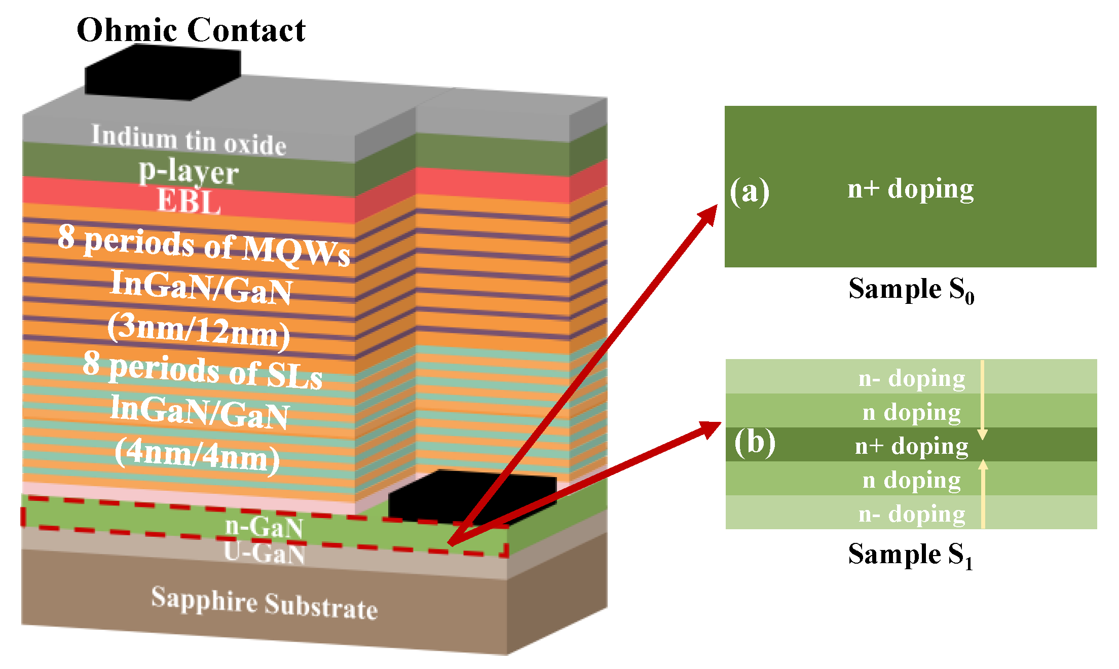
2. Materials and Methods

First of all, 25-nm-thick AlN nucleation layer is deposited on the sapphire substrates with magnetron sputtering on 2-inch (0001) patterned sapphire substrates. Following the nucleation layer, 2.4 μm-thick undoping GaN layer, Si-doping n-type GaN layer, 60 nm-thick Si-doping AlGaN layer as the first barrier, 8 periods of Al0.05Ga0.95N/GaN (4 nm/4 nm) SLs, 8 periods of InGaN/GaN (3 nm/12 nm) MQWs, 10 periods of 60 nm-thick Mg-doping GaN/Al0.15Ga0.85N (2.5 nm/3.5 nm) SLs as electron blocking layer and 200-nm-thick p-GaN layer are deposited by MOCVD successively. For our experiments, UV-LEDs with stair-like Si-doping GaN layers (Sample S1) are numerically investigated over UV-LEDs with heavily Si-doping GaN layers (Sample S0) counterpart. For Sample S0 with heavily Si-doping GaN layer, a 3 μm-thick GaN layer with the Si doping concentrations of 1 × 10 19 cm−3 is grown on the u-GaN layer. As for Sample S1, the stair-like Si-doping n-type GaN layers consists of five parts, namely 160 nm-thick GaN layer with 1.5 × 1018 cm−3 Si doping concentration, 400 nm-thick GaN layer with 3 × 1018 cm−3 Si doping concentration, 2000 nm-thick GaN layer with heavily 1 × 1019 cm−3 Si doping concentration, 400 nm-thick GaN layer with 1.5 × 1018 cm−3 Si doping concentration and 160 nm-thick GaN with 5 × 1017 cm−3 Si doping concentration. In order to demonstrate the effectiveness of the structure, the devices are fabricated (defined as Device S0 and Device S1) with Cr/Ni/Au multiple metal stacks deposited by e-beam evaporation serving as the p-contact and n-contact. Both of these wafers are then diced into individual chips with a dimension of 275 × 300 μm2. Two device structures are shown in Figure 1.
The atomic force microscopy (AFM) and high-resolution X-ray diffraction (HRXRD) are carried out to investigate the surface morphologies, crystalline quality of LEDs. Current-voltage (I-V), light output power (LOP) and wall plug efficiency (WPE) with injection current are also used to evaluate the photoelectric properties of the LEDs. In addition, light emission distribution test of LEDs and Advanced Physical Models of Semiconductor Devices software (APSYS) are adopted to reveal the mechanism of stair-like Si-doping structure to improve the current spreading character.

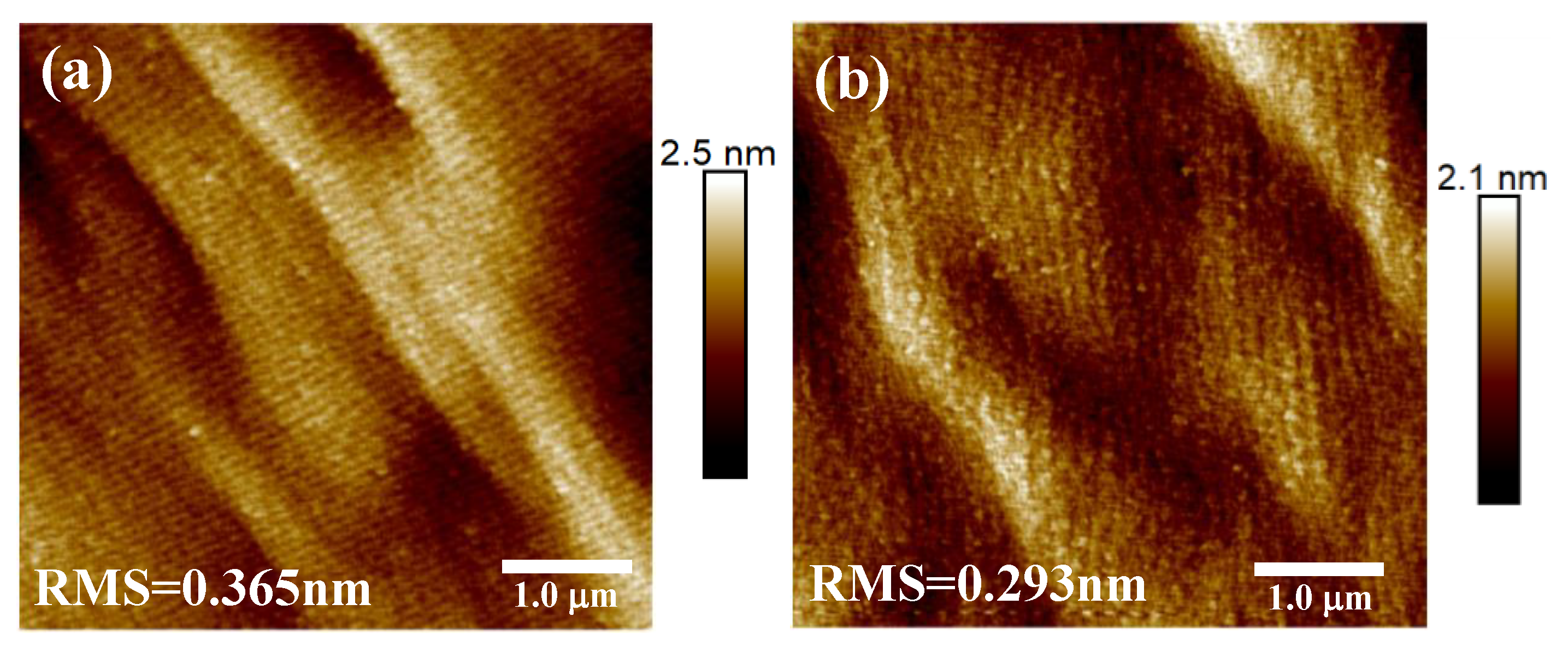
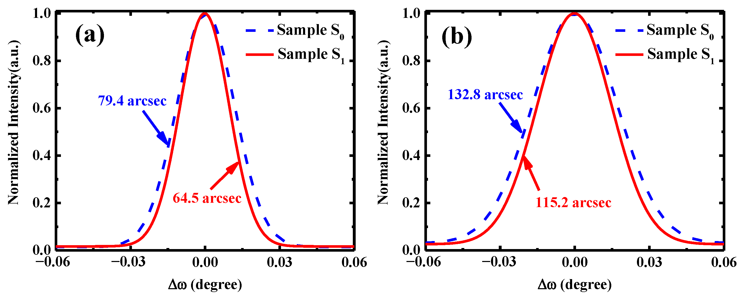
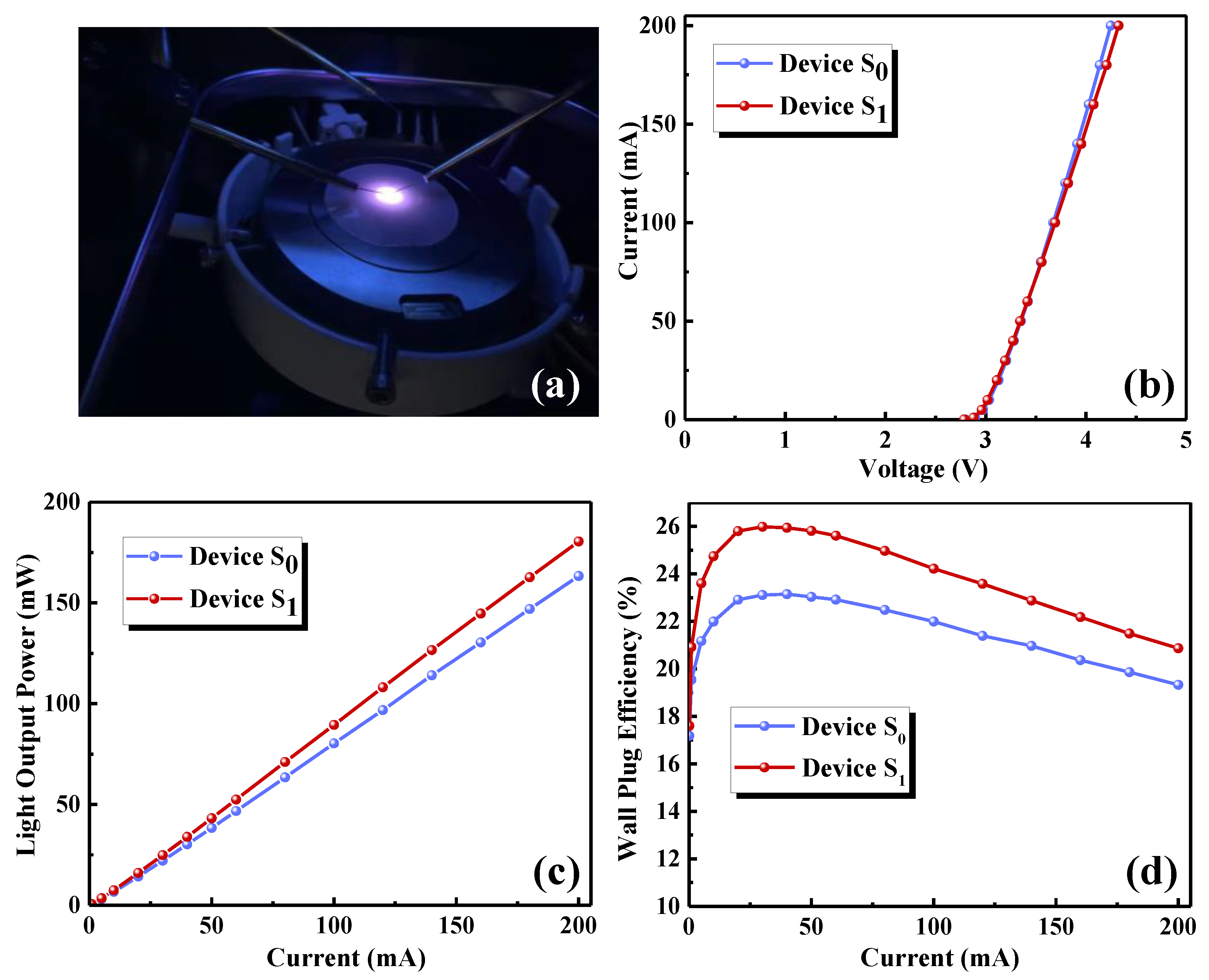
3. Results and Discussion

The 5 × 5 μm2 AFM images of Sample S0 and S1 are illustrated in Figure 2a,b. A smooth surface with distinct atomic step flow exists in Sample S0 and S1. Sample S1 exhibits a smoother surface with a lower root-mean-square (RMS) roughness than that of Sample S0 (0.365 nm for Sample S0 and 0.293 nm for Sample S1). The AFM images indicate that optimized method is beneficial to obtain smoother surface.
The HRXRD is adopted to investigate the crystal quality of epi-layers. Figure 3a,b show the X-ray rocking curves (XRCs) of both samples measured in symmetric (002) and asymmetric (102) reflection. The full width at half maximum (FWHM) of the (002) plane XRC is 64.5 arc sec of Sample S1, which is smaller than the FWHM value 79.4 arc sec of Sample S0, meanwhile the XRC-FWHM value for the (102) plane is significantly reduced from 132.8 arc sec (Sample S0) to 115.2 arc sec (Sample S1) by the adopted the stair-like Si-doping n-GaN epilayer. It is well known that the FWHM of symmetric (002) and (b) asymmetric (102) reflection is related to the density of screw and edge dislocations respectively [25]. The density of threading dislocation can be estimated from the full width at half maximum (FWHM) of GaN (002) and GaN (102) by the following equations [26]:
N s c r e w = β t i l t 2 4.35 b s 2
N e d g e = β t w i s t 2 4.35 b e 2
where b s and b e are the Burgers vectors of the screw dislocation (| b s |GaN = 0.5185 nm) and edge dislocation (| b e |GaN = 0.3189 nm). β t i l t and β t w i s t are the tilt and twist spread, respectively, which could be estimated by Equation (3):
β = ( β t i l t cos φ ) 2 + ( β t w i s t sin φ ) 2
where φ is the angle between the reciprocal lattice vector (Khkl) and the (001) plane normal. As such, the corresponding screw and edge dislocation densities are 1.27 × 107 cm−2 and 1.64 × 108 cm−2 for Sample S0, 8.36 × 106 cm−2 and 1.27 × 108 cm−2 for Sample S1, respectively. According to the results of HRXRD, such a conclusion could be draw that the employment of stair-like Si-doping structure reduces the dislocation density and effectively improves the crystalline quality.
To further investigate optoelectronic characteristic of UV-LEDs, two types of GaN-based LEDs with heavily and stair-like Si-doping n-type GaN are fabricated. Figure 4a shows the optical emission distribution of the Device S1 at 20 mA injected current. The I - V characteristics of both LEDs are shown in Figure 4b. LEDs with heavily and stair-like Si-doping n-type GaN have the similar turn-on voltages. Meanwhile, the operating current of Device S1 is slightly higher than that of Device S0 at high-voltage operations. This is attributed to the larger series resistance of Device S1, caused by the decreased conductivity of the lower Si doping level of n-GaN layer. Figure 4c reveals the integrated LOP as a function of the current injection of both LEDs. For both LEDs, the LOP is increased with increasing injection current up to 200 mA. It is noteworthy that Device S1 exhibits higher LOP than that of Device S0 across the whole current range. One possible reason for this is the reduction of dislocations. As one can see from Figure 3, there are much more dislocations in the Device S0 than that in Device S1 and those dislocations could act as non-radiative recombination centers. When electrons from n-GaN and holes from the p-GaN are injected into the active layers, they will recombine partially in the non-radiative recombination center, making the non-radiative recombination of Device S0 enhanced, thereby, the LOP of S0 is lower than that of Device S1; Another possible reason is that the potential barrier formed by the stair-like Si-doping n-type GaN layer enhances the current spreading horizontally. Figure 4d displays the WPEs as a function of the current injection of both LEDs. It is obvious that the Device S1 processes a better WPE than that of Device S0. The maximum WPEs of Device S1 and S0 are 26% and 23%, respectively. Both LEDs suffer from efficiency droop with injection current increases.
To verify the improvement of current spreading characteristic by introduction of stair-like Si-doping n-type GaN layer, microscopic light distribution test system (GMATG-M5) is adopted to collect the spatial distributions of light emission intensity of LEDs. Figure 5a,b show the normalized light emission intensity distribution images of Device S0 and S1 driven by 20 mA, respectively. Since the region with high current density corresponds to the area with high light emission intensity, the current density distribution in the chip can be inferred from the light emission intensity distribution of the LED chip. As seen in Figure 5a, the light emission intensity of Device S0 is mainly localized around the p-electrode edge. In contrast to Device S0, the light emission intensity is well distributed across the surface of Device S1. More uniform light emission intensity distribution indicates that the current spreading of Device S1 is superior to that of Device S0. The results support for the speculation of stair-like Si-doping n-type GaN layer in improving current spreading effectively. However, the mechanism responsible for the effect of stair-like Si-doping n-type GaN layer on current spreading still need to be discussed.
To further elucidate the role of stair-like Si-doping n-type GaN layer, the energy bands of the n-type region are calculated by the APSYS software [27]. The Shockley–Read–Hall recombination lifetime of 50 ns and Auger recombination coefficient 6.8 × 10⁻³⁰ cm6/s are set for non-radiative recombination in MQWs, respectively. In consideration of the screening by defects, the surface charges densities are set to be 40%. In addition, the conduction and valence band offset ratio for the InGaN/GaN alloy is set to 50/50 [28]. Figure 6a,b show the calculated energy band diagrams for the Device S0 and Device S1. Different from the flat band of Device S0, it could be found that there are two barriers (shown in the inset of Figure 6b) induced by the lower Si-doping concentration which is beneficial to the electron overflow reduction [29]. In addition, those two barriers will affect electrons transport, force electrons to spread horizontally and, finally, determine the carrier concentration in the MQWs [30]. In addition, research has shown that current spreading length is related to the sheet resistances of n-GaN layer [31]. By fitting the curves of Figure 4c, the series resistance of Device S0 and S1 was determined to be 5.7 Ω and 6.5 Ω, respectively. Namely, stair-like Si-doping concentration structure increases the layer resistivity vertically, making that the current extends in the horizontal direction. Briefly, the current spreading is improved.

4. Conclusions

In summary, the influence of Si-doping n-type GaN layer on the optoelectronic characteristic of LEDs are investigated. The GaN-based UV LED with stair-like Si-doping n-type GaN show a better crystal quality and optical properties than that with uniform heavily Si-doping GaN epitaxial layer. Compared with the LED with uniform heavily Si-doping GaN, LED with stair-like Si-doping n-type GaN presents higher LOP and WPE which is attributed to the reduction of dislocations and the enhancement of current lateral spreading characteristics by the introduction of stair-like Si-doping n-type GaN layer.

Author Contributions

Conceptualization, S.X. and X.F.; methodology, S.X. and X.F.; software, H.T.; validation, X.F.; formal analysis, S.X. and X.F.; investigation, X.F.; data curation, X.F.; writing—original draft preparation X.F.; writing—review and editing, X.F., H.T., R.P., J.D., Y.Z. and S.X.; funding acquisition, S.X., J.Z. (Jincheng Zhang), J.Z. (Jinfeng Zhang) and Y.H. All authors have read and agreed to the published version of the manuscript.

Funding

This research was funded by the Natural Science Foundation of China (Grant No. 62074120); the National Key R&D Program of China (2016YFB0400800, 2016YFB0400801); the WuHu and Xidian University Special Fund for Industry-University-Research cooperation (Grant No. XWYCXY-012020007); the State Key Laboratory on Integrated Optoelectronics (Grant No. IOSKL2018KF10), the Fundamental Research Funds for the Central Universities (Grant No. JB211108) and the Innovation Fund of Xidian University (YJS2011).

Acknowledgments

The authors express their thanks to the people helping with this work, and acknowledge the valuable suggestions from the peer reviewers.

Conflicts of Interest

The authors declare no conflict of interest.

References

  1. Tao, H.; Xu, S.; Zhang, J.; Li, P.; Lin, Z.; Hao, Y. Numerical investigation on the enhanced performance of N-polar AlGaN-based ultraviolet light-emitting diodes with superlattice p-type doping. IEEE Trans. Electron Devices 2019, 66, 478–484. [Google Scholar] [CrossRef]
  2. Taniyasu, Y.; Kasu, M.; Makimoto, T. An aluminium nitride light-emitting diode with a wavelength of 210 Nanometres. Nature 2006, 441, 325–328. [Google Scholar] [CrossRef] [PubMed]
  3. Su, H.; Xu, S.; Tao, H.; Fan, X.; Du, J.; Peng, R.; Zhao, Y.; Ai, L.; Wu, H.; Zhang, J.; et al. Improving the current spreading by Fe doping in n-GaN layer for GaN-based ultraviolet Light-emitting diodes. IEEE Trans. Electron Devices 2021, 42, 1346–1349. [Google Scholar] [CrossRef]
  4. Mukai, T.; Yamada, M.; Nakamura, S. Characteristics of InGaN-Based UV/Blue/Green/Amber/Red Light-Emitting Diodes. Jpn. J. Appl. Phys. 1999, 38, 3976–3981. [Google Scholar] [CrossRef]
  5. Feezell, D.F.; Schmidt, M.C.; DenBaars, S.P.; Nakamura, S. Development of nonpolar and semipolar InGaN/GaN visible light-emitting diodes. Mrs Bull 2009, 34, 318–323. [Google Scholar] [CrossRef]
  6. Chang, J.Y.; Huang, M.F.; Chen, F.M.; Liou, B.T.; Shih, Y.H.; Kuo, Y.K. Effects of quantum barriers and electron-blocking layer in deep-ultraviolet light-emitting diodes. J. Phys. D: Appl. Phys. 2018, 51, 075106. [Google Scholar] [CrossRef]
  7. Pozina, G.; Ciechonski, R.; Bi, Z.; Samuelson, L.; Monemar, B. Dislocation related droop in InGaN/GaN light emitting diodes investigated via cathodoluminescence. Appl. Phys. Lett. 2015, 107, 251106. [Google Scholar] [CrossRef] [Green Version]
  8. Liu, X.; Fan, G.; Zheng, S.; Gong, C.; Lu, T.; Zhang, Y.; Xu, Y.; Zhang, T. Investigation of GaN-based light-emitting diodes using a p-GaN/i-InGaN short-period superlattice structure as last quantum barrier. Sci China Tech. Sci. 2012, 56, 98–102. [Google Scholar] [CrossRef]
  9. Craven, M.D.; Waltereit, P.; Speck, J.S.; DenBaars, S.P. Well-width dependence of photoluminescence emission from a-plane GaN/AlGaN multiple quantum wells. Appl. Phys. Lett. 2004, 84, 496–498. [Google Scholar] [CrossRef]
  10. Chung, R.B.; Han, C.; Pan, C.C.; Pfaff, N.; Speck, J.S.; DenBaars, S.P.; Nakamura, S. The reduction of efficiency droop by Al0.82In0.18N/GaN superlattice electron blocking layer in (0001) oriented GaN-based light emitting diodes. Appl. Phys. Lett. 2012, 101, 131113. [Google Scholar] [CrossRef]
  11. Zhang, Y.Y.; Zhu, X.L.; Yin, Y.A.; Ma, J. Performance enhancement of near-UV light-emitting diodes with an InAlN/GaN superlattice electron-blocking layer. IEEE Trans. Electron Devices 2012, 33, 994–996. [Google Scholar] [CrossRef]
  12. Park, J.H.; Yeong Kim, D.; Hwang, S.; Meyaard, D.; Fred Schubert, E.; Dae Han, Y.; Won Choi, J.; Cho, J.; Kyu Kim, J. Enhanced overall efficiency of GaInN-based light-emitting diodes with reduced efficiency droop by Al composition-Graded AlGaN/GaN superlattice electron blocking layer. Appl. Phys. Lett. 2013, 103, 061104. [Google Scholar] [CrossRef] [Green Version]
  13. Gao, L.; Xie, F.; Yang, G. Numerical study of polarization-doped AlGaN ultraviolet light-emitting diodes. Superlattices Microstruct. 2014, 71, 1–6. [Google Scholar] [CrossRef]
  14. Wang, H.; Sodabanlu, H.; Daigo, Y.; Seino, T.; Nakagawa, T.; Sugiyama, M. Improved luminescence from InGaN/GaN MQWs by reducing initial nucleation density using sputtered AlN on sapphire substrate. J. Cryst. Growth 2017, 465, 12–17. [Google Scholar] [CrossRef]
  15. Lee, S.J.; Han, S.H.; Cho, C.Y.; Lee, S.P.; Noh, D.Y.; Shim, H.W.; Kim, Y.C.; Park, S.J. Improvement of GaN-based light-emitting diodes using p-type AlGaN/GaN superlattices with a graded Al composition. J. Phys. D: Appl. Phys. 2011, 44, 105101. [Google Scholar] [CrossRef] [Green Version]
  16. Sheremet, V.; Genc, M.; Elci, M.; Sheremet, N.; Aydinli, A.; Altuntas, I.; Ding, K.; Avrutin, V.; Ozgur, U.; Morkoc, H. The role of ITO resistivity on current spreading and leakage in InGaN/GaN light emitting diodes. Superlattices Microstruct. 2017, 111, 1177–1194. [Google Scholar] [CrossRef] [Green Version]
  17. Ali, A.H.; Abu Bakar, A.S.; Hassan, Z. Improved optoelectronics properties of ITO-based transparent conductive electrodes with the insertion of Ag/Ni under-layer. Appl. Surf. Sci 2014, 315, 387–391. [Google Scholar] [CrossRef] [Green Version]
  18. Liou, J.K.; Chen, C.C.; Chou, P.C.; Cheng, S.Y.; Tsai, J.H.; Liu, R.C.; Liu, W.-C. Effects of the use of an aluminum reflecting and an SiO2 insulating layers (RIL) on the performance of a GaN-based light-emitting diode with the naturally textured p-GaN surface. IEEE Trans. Electron Devices 2013, 60, 2282–2289. [Google Scholar] [CrossRef]
  19. Lee, J.; Kim, D.H.; Kim, K.S.; Seong, T.Y. Reducing forward voltage and enhancing output performance of InGaN-based blue light-emitting diodes using metal dot-embedded transparent p-type finger. Phys. Status Solidi A 2017, 214, 1600792. [Google Scholar] [CrossRef]
  20. Chen, K.Y.; Tien, C.H.; Hsu, C.P.; Pai, C.Y.; Horng, R.H. Fabrication and improved performance of GaN LEDs with finger-type structure. IEEE Trans. Electron Devices 2014, 61, 4128–4131. [Google Scholar] [CrossRef]
  21. Kolbe, T.; Knauer, A.; Rass, J.; Cho, H.K.; Mogilatenko, A.; Hagedorn, S.; Lobo Ploch, N.; Einfeldt, S.; Weyers, M. Improved efficiency of ultraviolet B light-emitting diodes with optimized p-side. Phys. Status Solidi A 2020, 217, 2000406. [Google Scholar] [CrossRef]
  22. Liu, H.H.; Chen, P.R.; Lee, G.Y.; Chyi, J.I. Efficiency enhancement of InGaN LEDs with an n-type AlGaN/GaN/InGaN current spreading layer. IEEE Electron Device Lett. 2011, 32, 1409–1411. [Google Scholar] [CrossRef]
  23. Song, H.; Jeon, K.S.; Hyoun, J.J.; Kim, S.; Lee, M.; Ah Lee, E.; Choi, H.; Sung, J.; Kang, M.-G.; Choi, Y.-H.; et al. Effects of enhanced lateral transport on InGaN/GaN light emitting diodes via n-type AlGaN/GaN superlattices. J. Appl. Phys. Lett. 2013, 103, 141102. [Google Scholar] [CrossRef]
  24. Kyaw, Z.; Zhang, Z.H.; Liu, W.; Tan, S.T.; Ju, Z.G.; Zhang, X.L.; Ji, Y.; Hasanov, N.; Zhu, B.; Lu, S.; et al. On the effect of n-GaN/p-GaN/n-GaN/p-GaN/n-GaN built-in junctions in the n-GaN layer for InGaN/GaN light-emitting diodes. Opt. Express 2014, 22, 809–816. [Google Scholar] [CrossRef] [PubMed] [Green Version]
  25. Heinke, H.; Kirchner, V.; Einfeldt, S.; Hommel, D. X-ray diffraction analysis of the defect structure in epitaxial GaN. Appl. Phys. Lett. 2000, 77, 2145–2147. [Google Scholar] [CrossRef]
  26. Pantha, B.N.; Dahal, R.; Nakarmi, M.L.; Nepal, N.; Li, J.; Lin, J.Y.; Jiang, H.X.; Paduano, Q.S.; Weyburne, D. Correlation between optoelectronic and structural properties and epilayer thickness of AlN. Appl. Phys. Lett. 2007, 90, 241101. [Google Scholar] [CrossRef] [Green Version]
  27. Zhang, Z.H.; Chen, S.W.H.; Chu, C.S.; Tian, K.K.; Fang, M.Q.; Zhang, R.H.; Bi, W.G.; Kuo, H.C. Nearly efficiency-droop-free AlGaN-based ultraviolet light-emitting diodes with a specifically designed superlattice p-type electron blocking layer for high Mg doping efficiency. Nanoscale Res. Lett. 2018, 13, 122. [Google Scholar] [CrossRef] [Green Version]
  28. Vurgaftman, I.; Meyer, J.R. Band parameters for nitrogen-containing semiconductors. J. Appl. Phys. 2003, 94, 3675–3696. [Google Scholar] [CrossRef]
  29. Yen, S.H.; Tsai, M.C.; Tsai, M.L.; Shen, Y.J.; Hsu, T.C.; Kuo, Y.K. Effect of n-type AlGaN layer on carrier transportation and efficiency droop of blue InGaN light-emitting diodes. IEEE Photonics Technol. Lett. 2009, 21, 975–977. [Google Scholar] [CrossRef]
  30. Lin, Z.; Wang, H.; Chen, S.; Lin, Y.; Yang, M.; Li, G.; Xu, B. Achieving high-performance blue GaN-based light-emitting diodes by energy band modification on AlxInyGa1 – x − yN electron blocking layer. IEEE Trans. Electron. Devices 2017, 64, 472–480. [Google Scholar] [CrossRef]
  31. Zhou, S.; Liu, M.; Hu, H.; Gao, Y.; Liu, X. Effect of ring-shaped SiO2 current blocking layer thickness on the external quantum efficiency of high power light-emitting diodes. Opt. Laser Technol. 2017, 97, 137–143. [Google Scholar] [CrossRef]
Figure 1. Schematic diagrams of (a) the reference device (Sample S0) and (b) the proposed device with stair-like Si-doping GaN layer (Sample S1).
Crystals 11 01203 g001
Figure 2. 5 × 5 μm2 AFM images for samples. The surface morphologies of (a) Sample S0 and (b) Sample S1.
Crystals 11 01203 g002
Figure 3. The XRCs of both samples measured in (a) symmetric (002) and (b) asymmetric (102) reflection.
Crystals 11 01203 g003
Figure 4. (a) the electroluminescence image of the Device S1; (b) I-V characteristic (c) the light output power and (d) WPE curve versus injection current of devices.
Crystals 11 01203 g004
Figure 5. The normalized light emission intensity distribution images of (a) Device S0 and (b) Device S1 at 20 mA.
Crystals 11 01203 g005
Figure 6. Energy band diagram for (a) the Device S0 and (b) Device S1, Ec, Ev, Efe and Efh denote as the conduction band, valance band and the quasi-Fermi level for electrons and holes, respectively. The inset exhibits the partial enlarged view of black dotted line frame.
Crystals 11 01203 g006
Publisher’s Note: MDPI stays neutral with regard to jurisdictional claims in published maps and institutional affiliations.

