
Growth of High Quality GaN on Si (111) Substrate by Using Two-Step Growth Method for Vertical Power Devices Application

1
Yield Enhancement Team, Foundry, Samsung Electronics Company Ltd., Yongin 17113, Korea
2
Advanced Material Research Center, Kumoh National Institute of Technology, Gumi 39177, Korea
*
Author to whom correspondence should be addressed.
Crystals 2021, 11(3), 234; https://0-doi-org.brum.beds.ac.uk/10.3390/cryst11030234
Submission received: 5 February 2021
/
Revised: 23 February 2021
/
Accepted: 25 February 2021
/
Published: 26 February 2021
(This article belongs to the Special Issue Nano/Micro and Bio-Inspired Materials on Wide-Bandgap-Semiconductor-Based Optoelectronic/Power Devices)
Abstract
:A crack-free GaN film grown on 4-inch Si (111) substrate is proposed using two-step growth methods simply controlled by both III/V ratio and pressure. Two-step growth process is found to be effective in compensating the strong tensile stress in the GaN layer grown on Si substrate. The high-resolution X-ray diffraction (XRD) rocking curves of (002) and (102) planes for the GaN epitaxial layer with two-step growth method are 317 and 432 arcsec, while the corresponding values for the reference sample without two-step growth method are 550 and 1207 arcsec, respectively. The reduced threading dislocation of GaN film with two-step growth method is obtained to be ~2 × 10⁸/cm2, which is attributed to effectively annihilate and bend threading dislocation.

1. Introduction
III–nitride semiconductors and related alloys are very promising materials for not only short wavelength optoelectronics (blue and green light-emitting diodes (LEDs), laser diodes (LDs)), but also high-power devices [1,2,3]. Because of several advantages of materials, such as wide band gap, high breakdown voltage, and high electron peak velocity, the AlGaN/GaN high electron mobility transistors (HEMTs) have an excellent potential for high-power and high-frequency devices application [4]. In order to grow a GaN epitaxial layer, silicon (Si) can be considered to a promising substrate due to its low cost and large wafer size compared to sapphire (Al2O3), silicon carbide (SiC), and GaN substrate [5]. However, the huge differences in lattice constant, crystal structure, and thermal expansion coefficient between GaN and Si are believed to be responsible for the difficulties in growing good quality GaN films on Si substrate. Especially, an amount of thermal (~56%) and lattice (~17%) mismatch make a large threading dislocation density (TDD) of 109~1010/cm2 in GaN grown on Si [6,7]. For successfully performing the growth of GaN on Si substrates, the AlN and AlGaN layers are typically used to mitigate the thermal and lattice mismatch at heterointerface of between GaN layer and Si wafer [6,7,8].
Another issue of the growth of GaN on Si substrate is hard to fabricate GaN vertical devices because the insulating property of AlN layer makes it challenging to realize the vertical current conduction, which results in significantly increasing the series resistance in GaN vertical devices. A thin AlN nucleation layer can be used for vertical conduction layer through tunneling mechanism [9]. Thus, to effectively obtain a vertical conduction, it is imperative to directly grow high quality GaN on a thin AlN nucleation layer and reduce dislocation densities [6].
In this work, we propose and grow a crack-free GaN film grown on Si substrate by using AIN buffer layer and two-step growth method, which consists of two growth steps; (1) first step is low growth rate with high III-V ratio/pressure and (2) second step is high growth rate with low III-V ratio/pressure in order to control stress and reduce dislocation density. The proposed growth method can be easily achieved to the GaN vertical device structure on Si substrates without the additional fabrication process, such as quasi-vertical structures, wafer bonding, and substrate removal techniques [10,11,12,13].
2. Experiments
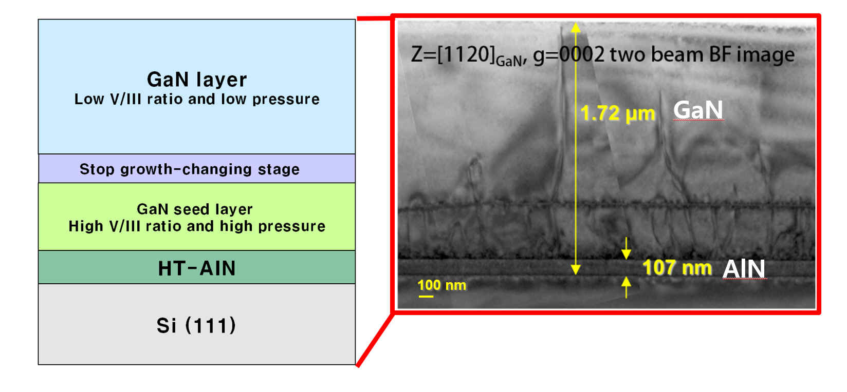
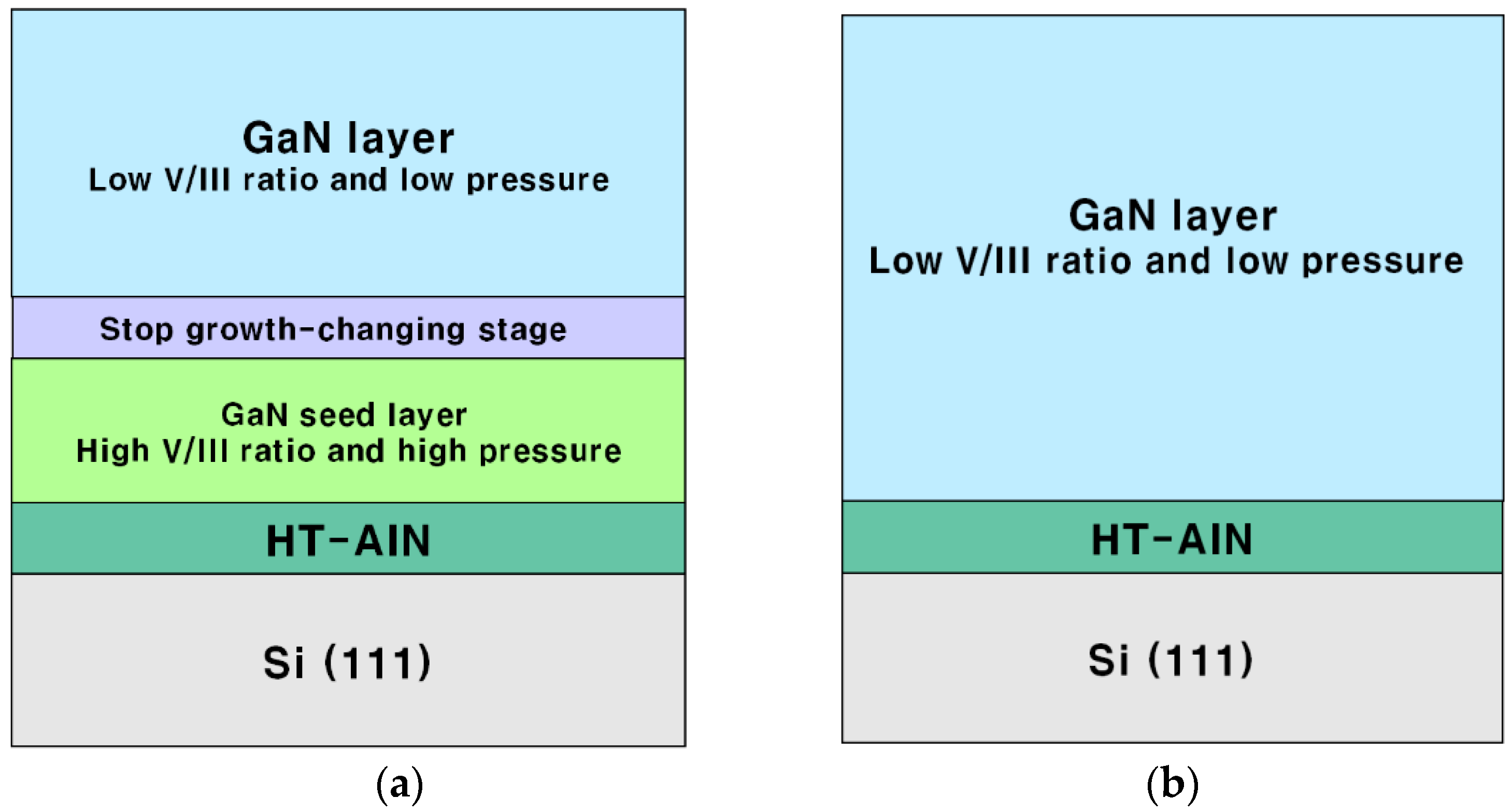
The GaN films were grown on 4-inch (111) p-type Si substrates by metal organic chemical vapor deposition (MOCVD). Trimethylgallium (TMGa), trimetahylaluminum (TMAl), and ammonia (NH3), were used for the precursors for Ga, Al, and N, respectively [14]. The Si substrate was baked in an H2 ambient at 1100 °C for 10 min to remove the native oxide prior to the growth of AlN buffer layer. Then, the Si surface was treated with Al pre-surface coverage during 60 seconds to suppress the formation of amorphous SiNx layer on the Si surface at the initial stage of growth [15]. The total layer structure with total thickness of approximate 1.7 μm consists of 100 nm-thick high temperature (HT)-AlN buffer layer, 400 nm-thick GaN seed layer, and 1.2 μm-thick GaN layer in growth sequence. The growth temperatures were set to be 1200 and 1150 °C for AlN and GaN layer, respectively. High quality GaN layer with reduced stress and dislocation density can be achieved by controlling the various growth conditions such as V-III ratio, pressure, and temperature. The detailed layer structure and growth conditions for samples are displayed in Figure 1 and the following processes. The GaN seed layer was grown on AIN buffer layer at the high V-III ratio of 15,000 and high pressure of 500 torr with low growth rate. To change both pressure and V-III ratio, the next stage is to stop the GaN growth for 3 min. Finally, the 1.2 μm-thick GaN was grown on GaN seed layer under low V-III ratio of 5000 and low pressure of 200 torr with high growth rate [16]. For comparison, the GaN with continuous V-III ratio of 5000 and pressure of 200 torr was also grown.
3. Results and Discussion
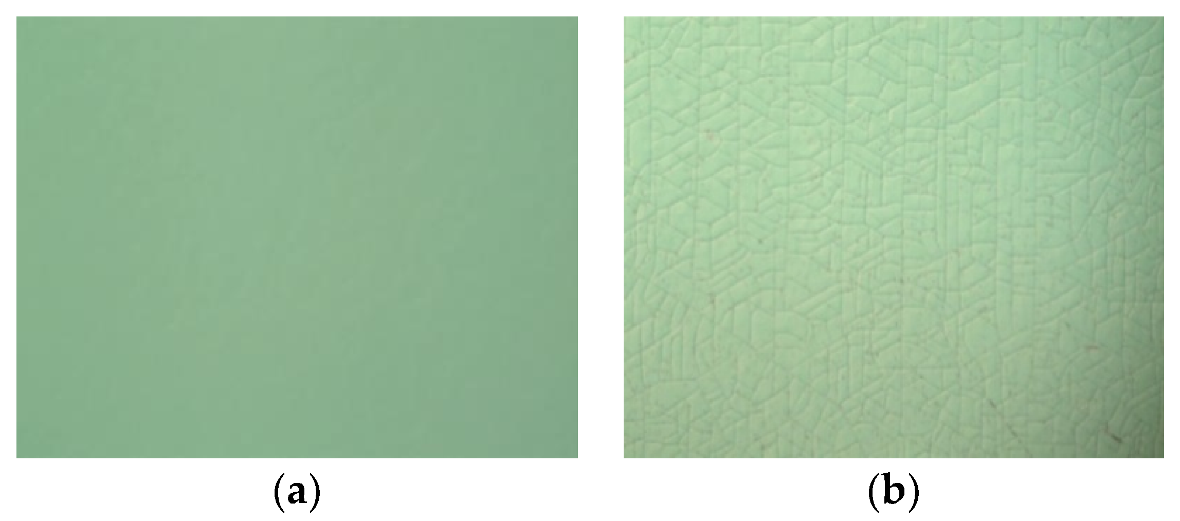
Figure 2 shows the optical microscopy images of GaN grown on Si substrate with and without two-step growth method to observe the surface morphology of the samples. The sample with two-step growth method exhibits the crack-free surface while the sample without two-step growth method presents many cracks on the surface. This explains that the two-step growth method is effective in compensating the tensile stress in the GaN layer grown on Si substrate, as discussed later.
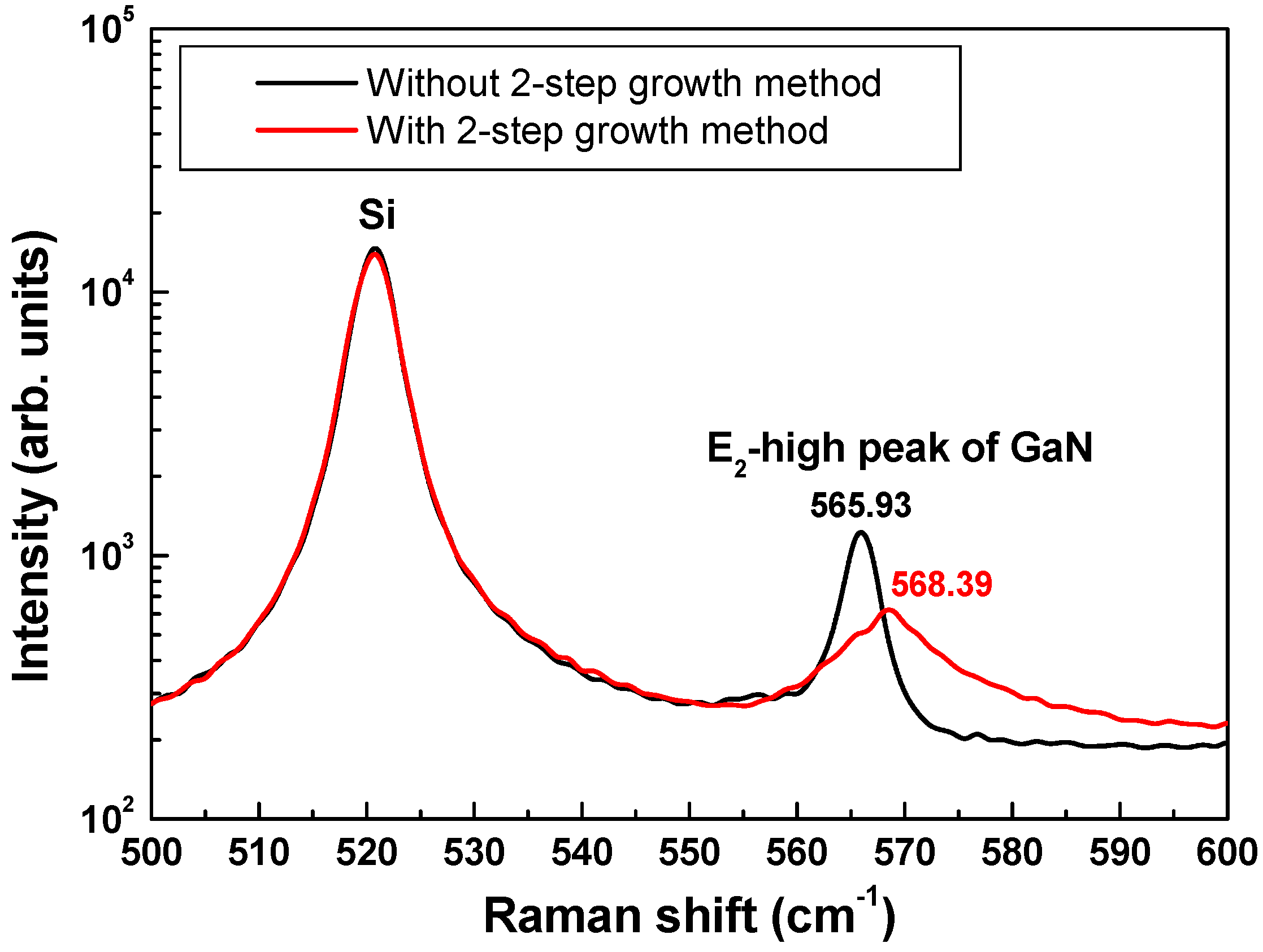
Raman scattering spectroscopy was investigated to elucidate the stress state of the grown GaN samples. As shown in Figure 3, the Raman scattering spectra exhibit peak shift at frequencies of 568.39 and 565.93 cm−1 for the grown films with and without the two-step growth method, corresponding to the calculated biaxial stresses of −0.201 and 0.397 GPa, respectively [17]. This indicates that the biaxial stress in the GaN grown on Si substrate with the two-step growth method is compressive while that without the two-step growth method still remains tensile, considering the reference value of 567.5 cm−1 for the freestanding GaN. It is believed that the two-step growth method gives rise to strong compressive stress in the GaN film grown on Si substrate during the high temperature growth, which sufficiently overcomes the tensile stress caused by cooling down and remains compressive even after completing the growth. On the other hand, the films without the two-step growth method were not able to significantly overwhelm the tensile stress, which results in the generation of crack on GaN surface due to different thermal expansion coefficient after cooling down.
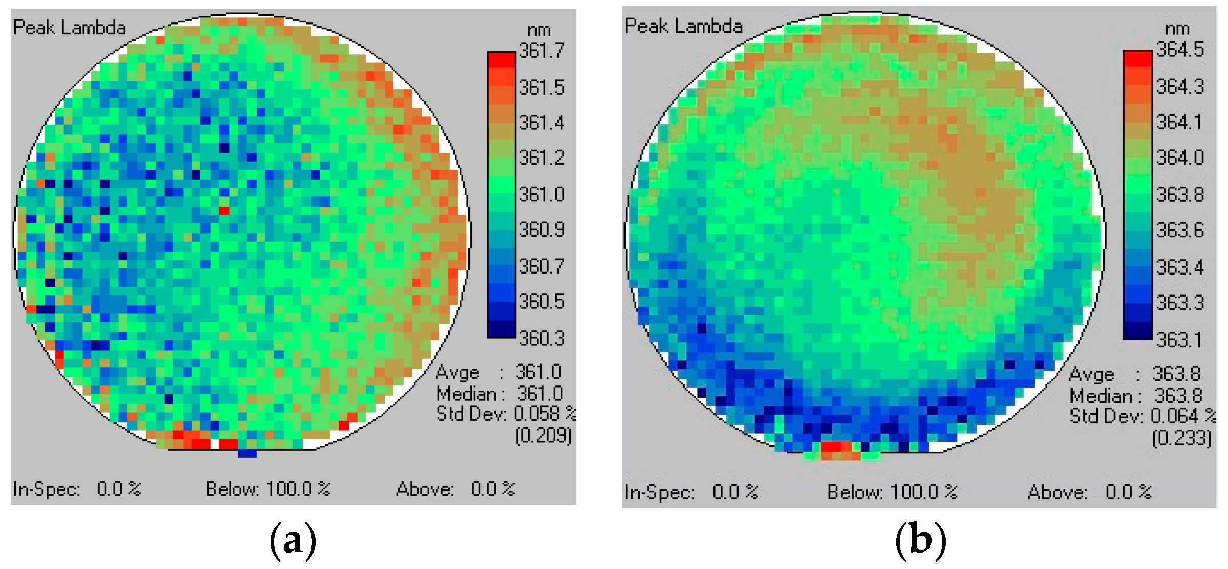
Figure 4 shows the photoluminescence (PL) mapping of GaN films grown on with and without the two-step growth method. The average PL spectral peak wavelength of the GaN film negatively shifts to 3 nm for the GaN film with the two-step growth method (361 nm) compared to the corresponding value for the GaN film without the two-step growth method (364 nm). This could be considered as direct evident that the GaN films with the two-step growth method well overcomes the tensile stress and hence exhibits the compressive strain, which is consistent with the Raman analysis in Figure 3.
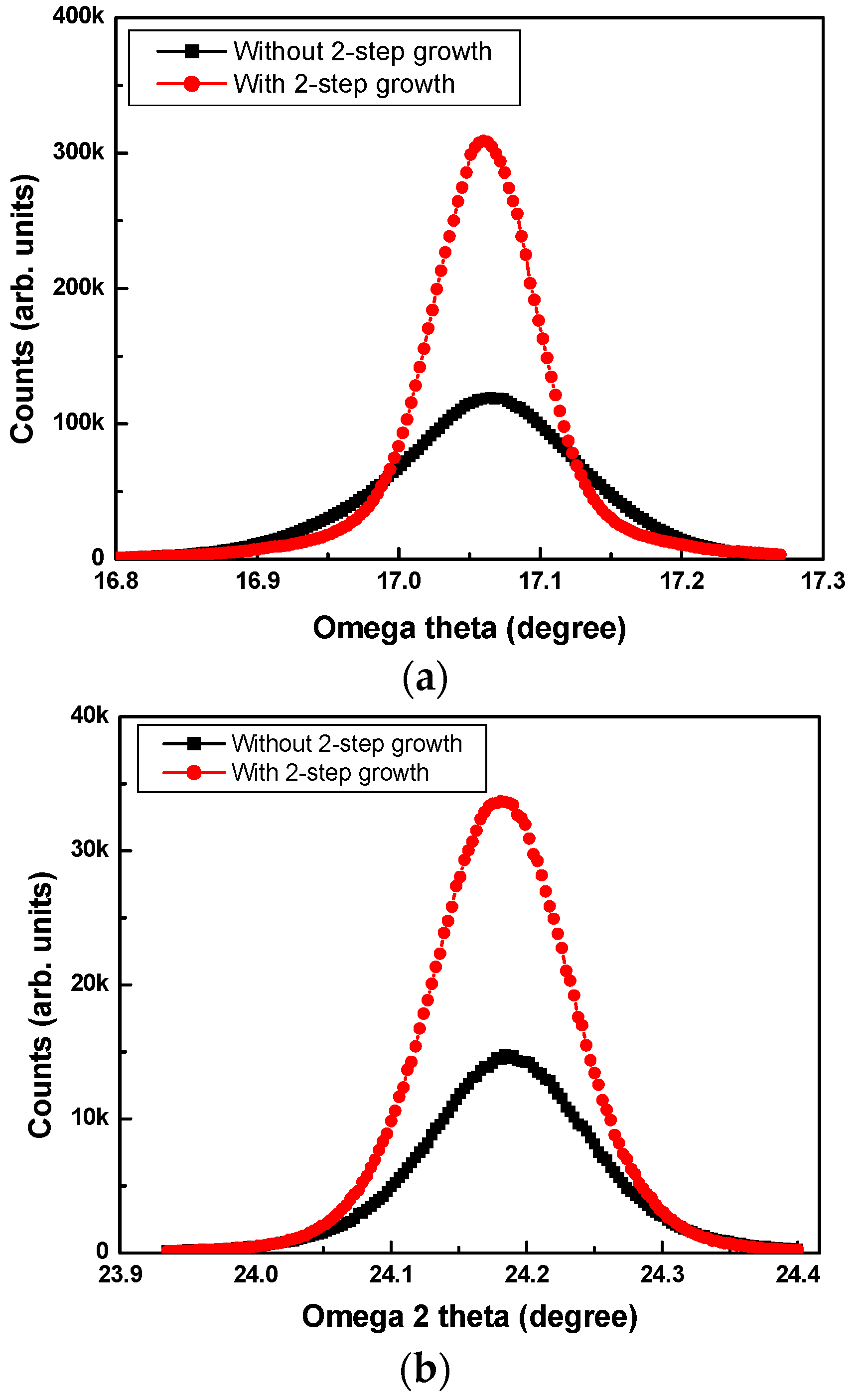
To further study the crystalline quality of the GaN layers, the crystal quality of 1.7 μm GaN epilayers was analyzed by high-resolution X-ray diffraction (HRXRD) measurements. The XRD rocking curves of symmetric (002) and asymmetric (102) planes are shown in Figure 5. The full width at half-maximum (FWHMs) of the (002) and (102) planes for the GaN epilayer with the two-step growth method are 317 and 432 arcsec, while those for GaN epilayer without the two-step growth method are 550 and 1207 arcsec, respectively. It is interesting that the value of FWHM (102) plane for the GaN epilayer with two-step growth is about three times lower than that of the (102) planes without two-step growth. Generally, the FWHMs are associated with TDD in GaN epilayer. This significant reduction of FWHMs means that the TDD of GaN epilayer with the two-step growth method is remarkably decreased.
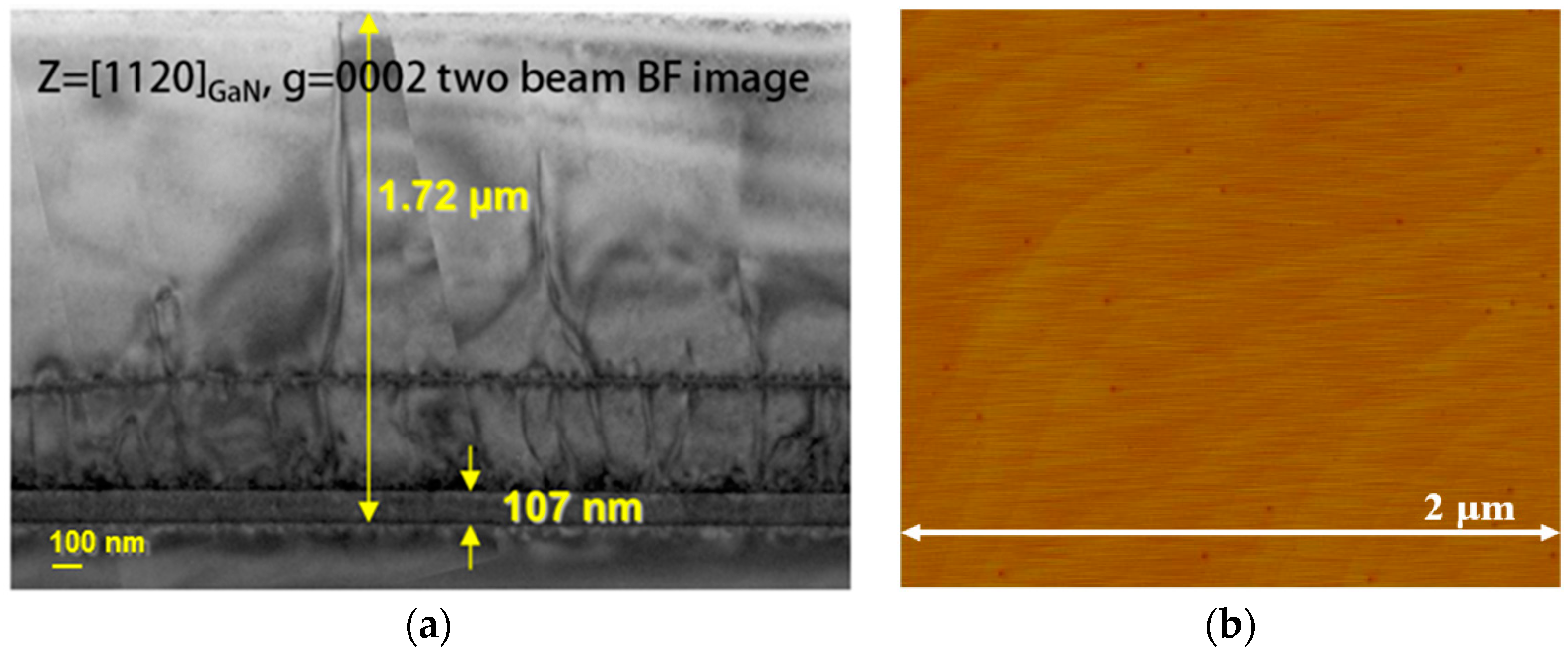
The cross-sectional transmission electron microscopy (TEM) image of the proposed sample in Figure 6a clearly exhibits the 100 nm-thick AIN buffer layer, 400 nm-thick GaN seed layer, and 1.2 μm-thick GaN layer, which are depicted in Figure 1a. This TEM image is taken along g = 000crystallographic direction in order to find the propagation behavior of the threading dislocation for GaN on Si. It also clearly observed that a lot of threading dislocation has been occurred in the GaN seed layer, which has been grown at low grow rate and high V-III ratio/pressure to obtain 2-dimensional (2-D) growth. However, the density of threading dislocation dramatically reduces in GaN layer grown at condition of low V-III ratio and low pressure. On the other hand, it is known that many threading dislocations generate in the GaN seed layer and propagate to the whole thick GaN buffer layer in the literatures [9,18]. The TDD can be obtained to calculate by counting the pits on the TEM and/or AFM images and then averaging them. The estimated TDD is ~8 × 10⁸/cm2 and ~2 × 10⁸/cm2 for the seed GaN and the thick GaN layer, respectively. The root mean square (RMS) roughness of GaN with two-step growth obtained by atomic force microscopy (AFM) is 0.12 nm, as shown in Figure 6b. From the dark points in GaN surface observed in AFM image, the TDD is also extracted to 2 × 10⁸/cm2, which value is well matched with that of the threading dislocation indicated by the cross-section TEM image. The two-step growth method seems to be effective in reducing threading dislocation. The dislocation density is related to the grain size and stress relaxation [6]. The initial GaN seed layer with low growth rate (grown at the high V-III ratio/pressure) makes the small grain size and large nuclei densities, which leads to the high dislocations formed at the grain boundary. The following step under low V-III ratio/pressure with high growth rate introduce large size of grain with high compressive stress, which results in annihilating and bending threading dislocation [16,19]. The interval of stop-growth, which change the pressure and growth rate, is also helpful to reduce and minimize threading dislocations.
4. Conclusions
We propose a crack-free GaN film on Si substrate by using the two-step growth method. This method occurs a compressive stress in total GaN epitaxial layer, which compensates the strong tensile stress in the underlaying GaN seed layer and hence results in crack-free film growth. Especially, the interval of stop-growth (changing pressure and growth rate) results in annihilating and bending threading dislocation, which leads to the effectively reduced the dislocation density of ~2 × 10⁸/cm2 for GaN film with the two-step growth method. This technique would have great application potential for the growth and fabrication of fully vertical GaN device on Si substrates.
Author Contributions
Writing-review and editing, J.-H.L. and K.-S.I.; investigation, J.-H.L. and K.-S.I.; synthesis, J.-H.L., K.-S.I.; data collection of Raman and XRD, K.-S.I. All authors have read and agreed to the published version of the manuscript.
Funding
This research received no external funding.
Institutional Review Board Statement
Not applicable.
Informed Consent Statement
Not applicable.
Data Availability Statement
Not applicable.
Acknowledgments
This work was supported by the National Research Foundation of Korea (NRF) funded by the Ministry of Education, Science and Technology (MEST) (No. NRF-2018R1A6A1A03025761, NRF-2019R1I1A1A01064011).
Conflicts of Interest
The authors declare no conflict of interest.
References
- Uemoto, Y.; Hikita, M.; Ueno, H.; Matsuo, H.; Ishida, H.; Yanagihara, M.; Ueda, T.; Tanaka, T.; Ueda, D. Gate injection transistor (GIT)-A normally-off AlGaN/GaN power transistor using conductivity modulation. IEEE Trans. Electron Devices 2007, 54, 3393. [Google Scholar] [CrossRef]
- Lee, J.-H.; Lee, D.Y.; Oh, B.W.; Lee, J.-H. Comparison of InGaN-based LEDs grown on conventional sapphire and cone-shape-patterned sapphire substrate. IEEE Trans. Electron Devices 2010, 57, 157. [Google Scholar] [CrossRef]
- Lee, J.-H.; Lee, J.-H. Abnormal Electrical and Optical Characteristics of InGaN-Based LEDs by Current Stress-Time-Dependent Annihilation. IEEE J. Quantum Electron. 2012, 48, 635. [Google Scholar] [CrossRef]
- Wu, Y.-F.; Kapolnek, D.; Ibbetson, J.P.; Parikh, P.; Keller, B.P.; Mishra, U.K. Very-high power density AlGaN/GaN HEMTs. IEEE Trans. Electron Devices 2001, 48, 586. [Google Scholar]
- Semond, F.; Lorenzini, P.; Grandjean, N.; Massies, J. High electron mobility AlGaN/GaN heterostructures grown on Si(111) by molecular beam epitaxy. Appl. Phys. Lett. 2001, 82, 335. [Google Scholar] [CrossRef]
- Wang, K.; Li, M.D.; Yang, Z.J.; Wu, J.J.; Yu, T.J. Stress control and dislocation reduction in the initial growth of GaN on Si (111) substrates by using a thin GaN transition layer. CrystEngComm 2019, 21, 4792. [Google Scholar] [CrossRef]
- Ma, J.; Zhu, X.; Wong, K.M.; Zou, X.; Lau, K.M. Improved GaN-based LED grown on silicon (111) substrates using stress/dislocation-engineered interlayers. J. Cryt. Growth 2013, 370, 265. [Google Scholar] [CrossRef]
- Cheng, K.; Leys, M.; Degroote, S.; Daele, B.; Boeykens, S.; Derluyn, J.; Germain, M.; Tendeloo, G.; Engelen, J.; Borghs, G. Flat GaN Epitaxial Layers Grown on Si(111) by Metalorganic Vapor Phase Epitaxy Using Step-Graded AlGaN Intermediate Layers. J. Electron. Mater. 2006, 35, 592. [Google Scholar] [CrossRef]
- Egawa, T.; Moku, T.; Ishikawa, H.; Ohtsuka, K.; Jimbo, T. Improved Characteristics of Blue and Green InGaN-Based Light-Emitting Diodes on Si Grown by Metalorganic Chemical Vapor Deposition. Jpn. J. Appl. Phys. 2002, 41, L663. [Google Scholar] [CrossRef]
- Zhang, Y.; Sun, M.; Piedra, D.; Azize, M.; Zhang, X.; Fujishima, T.; Palacios, T. GaN-on-Si Vertical Schottky and p-n Diodes. IEEE Electron Device Lett. 2014, 35, 618. [Google Scholar]
- Khadar, R.A.; Liu, C.; Zhang, L.; Xiang, P.; Cheng, K.; Matioli, E. 820-V GaN-on-Si Quasi-Vertical p-i-n Diodes With BFOM of 2.0 GW/cm2. IEEE Electron Device Lett. 2018, 39, 401. [Google Scholar] [CrossRef] [Green Version]
- Zou, X.; Zhang, X.; Lu, X.; Tang, C.W.; Lau, K.M. Fully Vertical GaN p-i-n Diodes Using GaN-on-Si Epilayers. IEEE Electron Device Lett. 2016, 37, 636. [Google Scholar] [CrossRef]
- Zhang, E.; Yuan, M.; Chowdhury, N.; Cheng, K.; Palacios, T. 720-V/0.35-mcm2 Fully Vertical GaN-on-Si Power Diodes by Selective Removal of Si Substrates and Buffer Layers. IEEE Electron Device Lett. 2018, 39, 715. [Google Scholar] [CrossRef]
- Lee, J.H.; Park, C.; Kim, K.W.; Kim, D.S.; Lee, J.-H. Performance of fully recessed AlGaN/GaN MOSFET prepared on GaN buffer layer grown with AlSiC precoverage on silicon substrate. IEEE Electron Device Lett. 2013, 34, 975. [Google Scholar] [CrossRef]
- Chen, P.; Zhang, R.; Zhao, Z.; Xi, D.; Shen, B.; Chen, Z.; Zhou, Y.; Xie, S.; Lu, W.; Zheng, Y. Growth of high quality GaN layers with AIN buffer on Si(111) substrates. J. Cryst. Growth 2001, 225, 2. [Google Scholar] [CrossRef]
- Lee, J.H.; Lee, J.H.; Cho, H.I. Nitride Based Semiconductor Device and Process for Preparing the Same. U.S. Patent No. 7319064 B2, 15 January 2008. [Google Scholar]
- Tripathy, S.; Chua, S.J.; Chen, P.; Miao, Z.L. Micro-Raman investigation of strain in GaN and AlxGa1−xN/GaN heterostructures grown on Si (111). J. Appl. Phys. 2002, 92, 3503. [Google Scholar] [CrossRef]
- Langea, A.P.; Mahajan, S. Influence of trimethylaluminum predoses on the growth morphology, filmsubstrate interface, and microstructure of MOCVD-grown AlN on (111) Si. J. Cryst. Growth 2019, 511, 106. [Google Scholar] [CrossRef]
- Lee, J.-H.; Lee, M.-B.; Hahm, S.-H.; Lee, Y.-H.; Lee, J.-H.; Bae, Y.-H.; Cho, H.K. Growth of Semi-insulating GaN Layer by Controlling Size of Nucleation Sites for SAW Device Applications. MRS Internet J. Nitride Semicond. Res. 2003, 8, 5. [Google Scholar] [CrossRef]
Figure 1.
Schematic cross-sectional view of structure for GaN grown on Si substrate (a) with and (b) without two-step growth method.
Figure 1.
Schematic cross-sectional view of structure for GaN grown on Si substrate (a) with and (b) without two-step growth method.

Figure 2.
Optical microscopy images (1 mm × 1 mm) of GaN grown on Si substrate (a) with and (b) without the two-step growth method.
Figure 2.
Optical microscopy images (1 mm × 1 mm) of GaN grown on Si substrate (a) with and (b) without the two-step growth method.

Figure 3.
Raman spectra of GaN grown on Si substrate with and without the two-step growth method.

Figure 4.
PL mapping of GaN grown on Si substrate (a) with and (b) without the two-step growth method.
Figure 4.
PL mapping of GaN grown on Si substrate (a) with and (b) without the two-step growth method.

Figure 5.
(a) Symmetric (002) and (b) asymmetric (102) rocking curves GaN grown on Si substrate with and without the two-step growth method.
Figure 5.
(a) Symmetric (002) and (b) asymmetric (102) rocking curves GaN grown on Si substrate with and without the two-step growth method.

Figure 6.
(a) TEM and (b) AFM images of GaN grown on Si substrate with the two-step growth method.

Publisher’s Note: MDPI stays neutral with regard to jurisdictional claims in published maps and institutional affiliations. |
© 2021 by the authors. Licensee MDPI, Basel, Switzerland. This article is an open access article distributed under the terms and conditions of the Creative Commons Attribution (CC BY) license (http://creativecommons.org/licenses/by/4.0/).
Share and Cite
MDPI and ACS Style
Lee, J.-H.; Im, K.-S. Growth of High Quality GaN on Si (111) Substrate by Using Two-Step Growth Method for Vertical Power Devices Application. Crystals 2021, 11, 234. https://0-doi-org.brum.beds.ac.uk/10.3390/cryst11030234
AMA Style
Lee J-H, Im K-S. Growth of High Quality GaN on Si (111) Substrate by Using Two-Step Growth Method for Vertical Power Devices Application. Crystals. 2021; 11(3):234. https://0-doi-org.brum.beds.ac.uk/10.3390/cryst11030234
Chicago/Turabian StyleLee, Jae-Hoon, and Ki-Sik Im. 2021. "Growth of High Quality GaN on Si (111) Substrate by Using Two-Step Growth Method for Vertical Power Devices Application" Crystals 11, no. 3: 234. https://0-doi-org.brum.beds.ac.uk/10.3390/cryst11030234
Note that from the first issue of 2016, this journal uses article numbers instead of page numbers. See further details here.