
Electric Double Layer Doping of Charge-Ordered Insulators α-(BEDT-TTF)2I3 and α-(BETS)2I3

 , and
, and 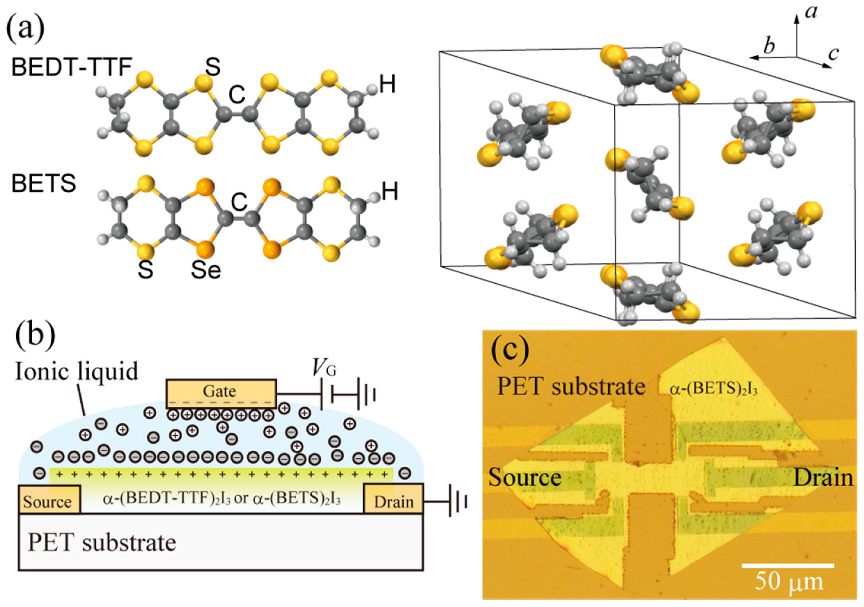
Abstract
:1. Introduction
2. Materials and Methods
3. Results
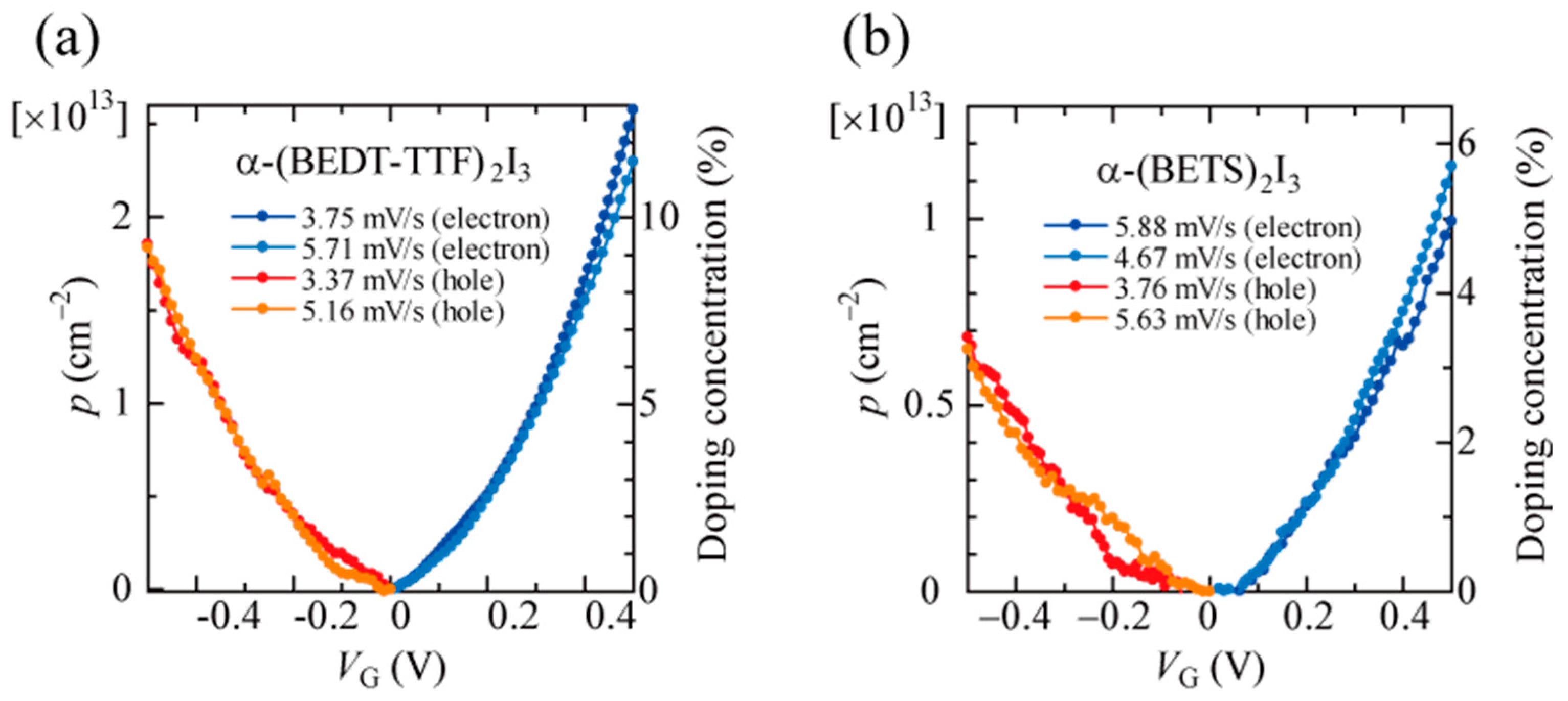
3.1. Charge Displacement Current Measurement
3.2. Temperature Dependence of Resistance at Various Gate Voltages
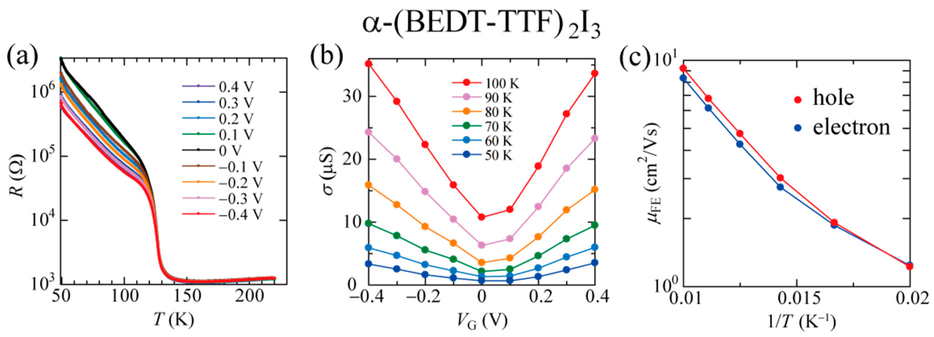
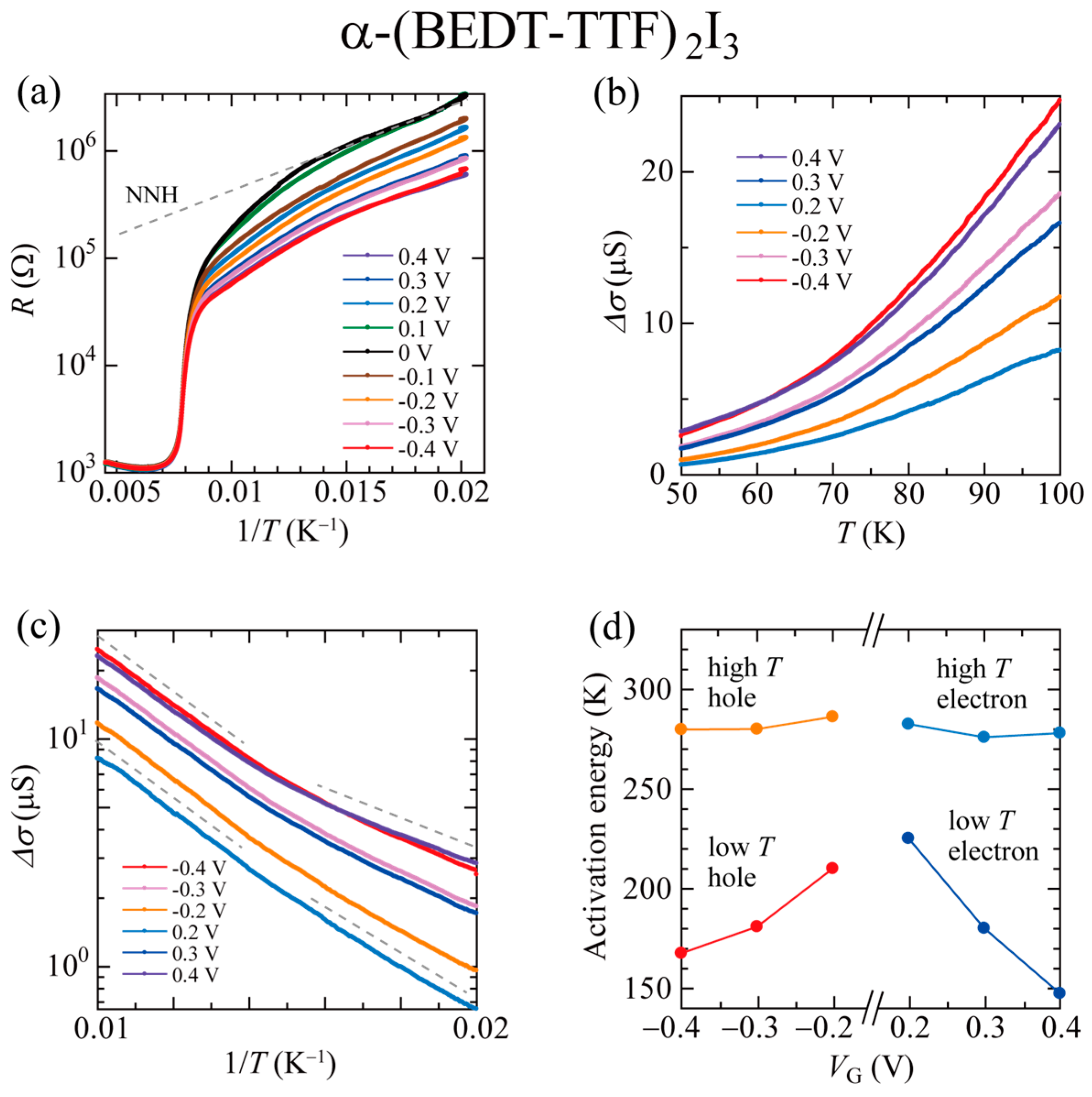
3.2.1. α-(BEDT-TTF)2I3
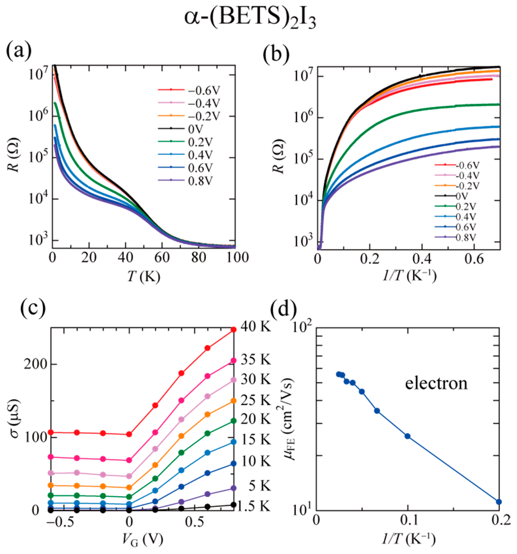
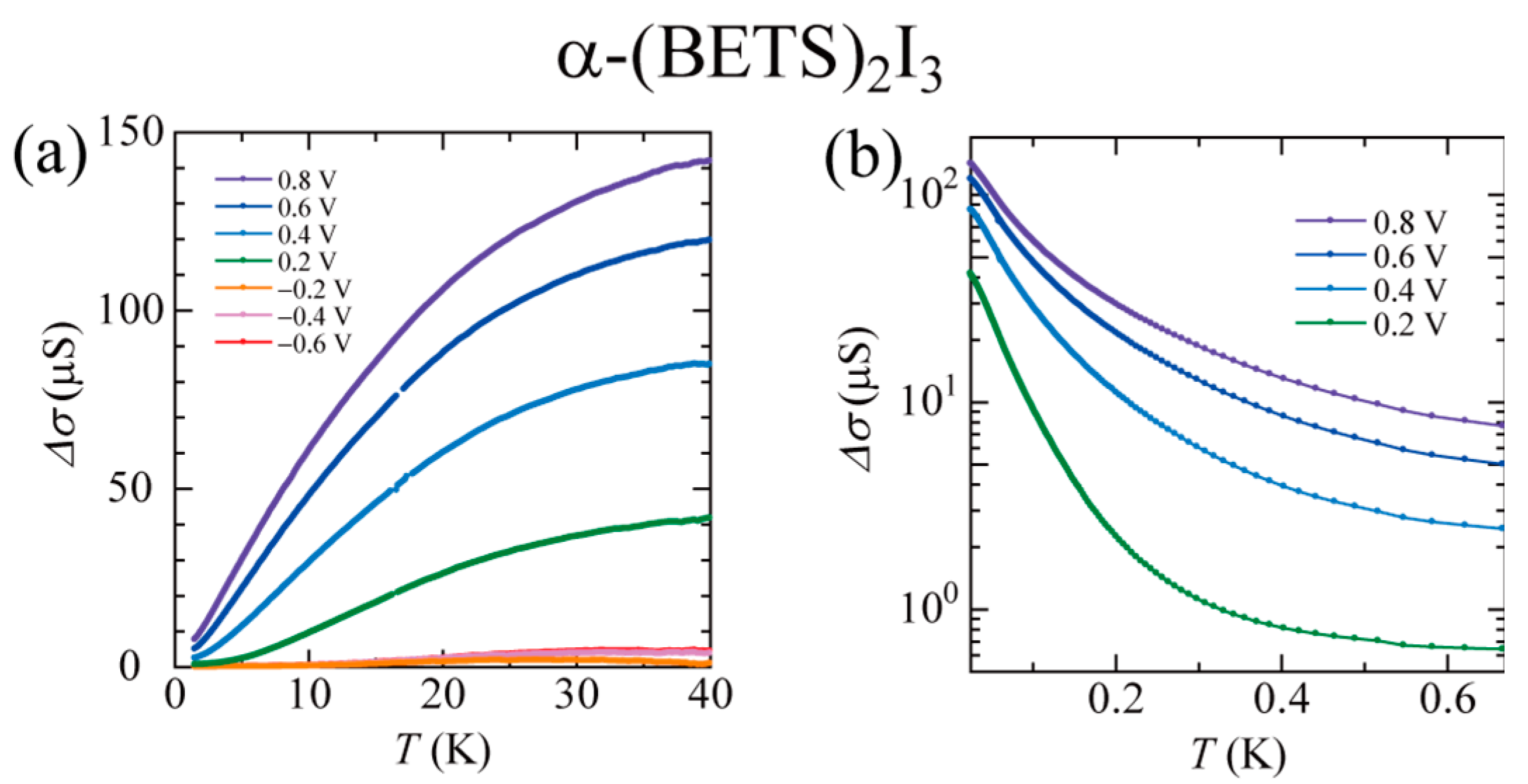
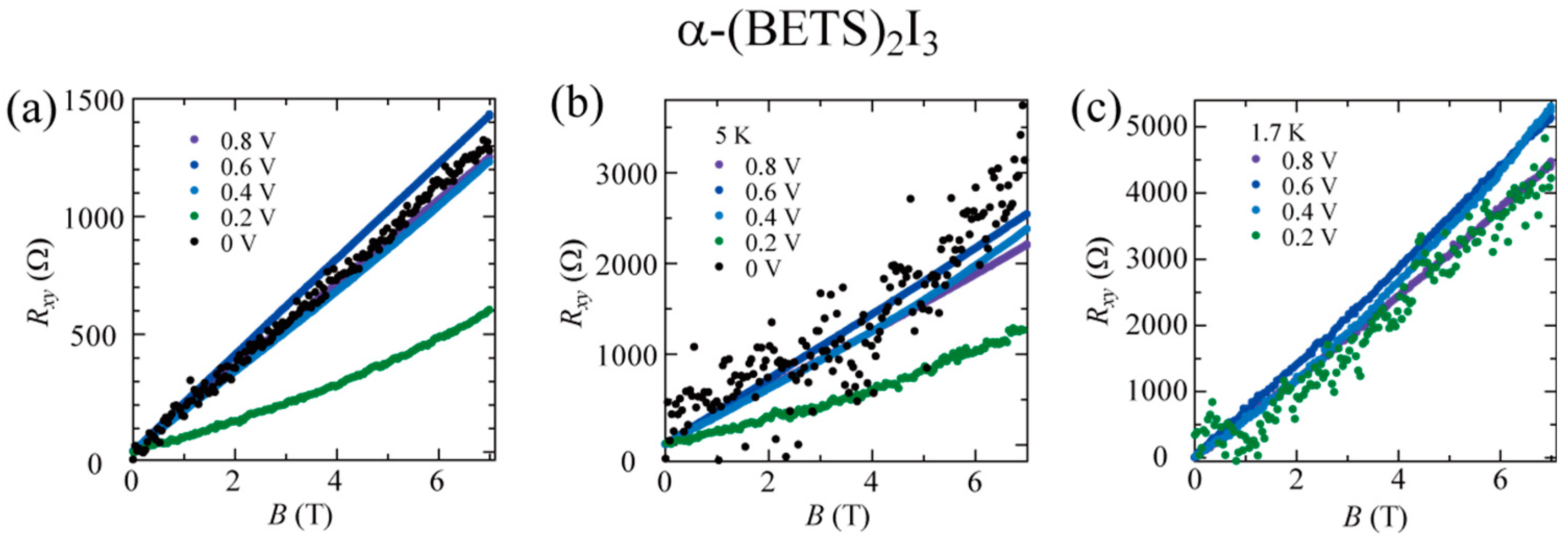
3.2.2. α-(BETS)2I3
4. Discussion and Conclusions
Author Contributions
Funding
Informed Consent Statement
Data Availability Statement
Acknowledgments
Conflicts of Interest
References
- Imada, M.; Fujimori, A.; Tokura, Y. Metal-insulator transitions. Rev. Mod. Phys. 1998, 70, 1039–1263. [Google Scholar] [CrossRef] [Green Version]
- Ahn, C.H.; Bhattacharya, A.; Di Ventra, M.; Eckstein, J.N.; Frisbie, C.D.; Gershenson, M.E.; Goldman, A.M.; Inoue, I.H.; Mannhart, J.; Millis, A.J.; et al. Electrostatic modification of novel materials. Rev. Mod. Phys. 2006, 78, 1185–1212. [Google Scholar] [CrossRef] [Green Version]
- Fujimoto, T.; Awaga, K. Electric-double-layer field-effect transistors with ionic liquids. Phys. Chem. Chem. Phys. 2013, 15, 8983–9006. [Google Scholar] [CrossRef] [PubMed]
- Ueno, K.; Shimotani, H.; Yuan, H.; Ye, J.; Kawasaki, M.; Iwasa, Y. Field-induced superconductivity in electric double layer transistors. J. Phys. Soc. Jpn. 2014, 83, 032001. [Google Scholar] [CrossRef]
- Yamamoto, H.M.; Nakano, M.; Suda, M.; Iwasa, Y.; Kawasaki, M.; Kato, R. A strained organic field-effect transistor with a gate-tunable superconducting channel. Nat. Commun. 2013, 4, 2379. [Google Scholar] [CrossRef] [Green Version]
- Kawasugi, Y.; Seki, K.; Tajima, S.; Pu, J.; Takenobu, T.; Yunoki, S.; Yamamoto, H.M.; Kato, R. Two-dimensional ground-state mapping of a Mott-Hubbard system in a flexible field-effect device. Sci. Adv. 2019, 5, eaav7278. [Google Scholar] [CrossRef] [Green Version]
- Yamamoto, H.M.; Ito, H.; Ikeda, M.; Kato, R.; Shigeto, K.; Tsukagoshi, K. Nano-size molecular conductors directly formed on silicon substrates. In Multifunctional Conducting Molecular Materials; Royal Society of Chemistry: London, UK, 2006; pp. 97–100. [Google Scholar]
- Yamamoto, H.M.; Hosoda, M.; Kawasugi, Y.; Tsukagoshi, K.; Kato, R. Field effect on organic charge-ordered/Mott insulators. Physica B 2009, 404, 413–415. [Google Scholar] [CrossRef] [Green Version]
- Kimata, M.; Ishihara, T.; Tajima, H. Electrostatic charge carrier injection into the charge-ordered organic material α-(BEDT-TTF)2I3. J. Phys. Soc. Jpn. 2012, 81, 073704. [Google Scholar] [CrossRef]
- Kimata, M.; Ishihara, T.; Ueda, A.; Mori, H.; Tajima, H. Fabrication of a field effect transistor structure using charge-ordered organic materials α-(BEDT-TTF)2I3 and α’-(BEDT-TTF)2IBr2. Synth. Met. 2013, 173, 43–45. [Google Scholar] [CrossRef]
- Bender, K.; Hennig, I.; Schweitzer, D.; Dietz, K.; Endres, H.; Keller, H.J. Synthesis, Structure and Physical Properties of a Two-Dimensional Organic Metal, Di[bis(ethylenedithiolo)tetrathiofulvalene] triiodide, (BEDT-TTF)+2I−3. Mol. Cryst. Liq. Cryst. 1984, 108, 359–371. [Google Scholar] [CrossRef] [Green Version]
- Tajima, N.; Sugawara, S.; Tamura, M.; Nishio, Y.; Kajita, K. Electronic phases in an organic conductor α-(BEDT-TTF)2I3: Ultra narrow gap semiconductor, superconductor, metal, and charge-ordered insulator. J. Phys. Soc. Jpn. 2006, 75, 051010. [Google Scholar] [CrossRef] [Green Version]
- Inokuchi, M.; Tajima, H.; Kobayashi, A.; Ohta, T.; Kuroda, H.; Kato, R.; Naito, T.; Kobayashi, H. Electrical and optical properties of α-(BETS)2I3 and α-(BEDT-STF)2I3. Bull. Chem. Soc. Jpn. 1995, 68, 547–553. [Google Scholar] [CrossRef]
- Kitou, S.; Tsumuraya, T.; Sawahata, H.; Ishii, F.; Hiraki, K.; Nakamura, T.; Katayama, N.; Sawa, H. Ambient-pressure Dirac electron system in the quasi-two-dimensional molecular conductor α-(BETS)2I3. Phys. Rev. B 2021, 103, 035135. [Google Scholar] [CrossRef]
- Ohki, D.; Yoshimi, K.; Kobayashi, A. Transport properties of the organic Dirac electron system α-(BEDT-TSeF)2I3. Phys. Rev. B 2021, 102, 235116. [Google Scholar] [CrossRef]
- Tsumuraya, T.; Suzumura, Y. First-principles study of the effective Hamiltonian for Dirac fermions with spin-orbit coupling in two-dimensional molecular conductor α-(BETS)2I3. Eur. Phys. J. B 2021, 94, 17. [Google Scholar] [CrossRef]
- Xie, W.; Frisbie, C.D. Organic electrical double layer transistors based on rubrene single crystals: Examining transport at high surface charge densities above 1013 cm−2. J. Phys. Chem. Rev. 2011, 115, 14360–14368. [Google Scholar] [CrossRef]
- Kawasugi, Y.; Yamamoto, H.M.; Hosoda, M.; Tajima, N.; Fukunaga, T.; Tsukagoshi, K.; Kato, R. Strain-induced superconductor/insulator transition and field effect in a thin single crystal of molecular conductor. Appl. Phys. Lett. 2008, 92, 243508. [Google Scholar] [CrossRef]
- Ivek, T.; Čulo, M. Semimetallic and charge-ordered α-(BEDT-TTF)2I3: On the role of disorder in dc transport and dielectric properties. Phys. Rev. B 2017, 96, 075141. [Google Scholar] [CrossRef] [Green Version]
- Kravchenko, S.V.; Kravchenko, G.V.; Furneaux, J.E.; Pudalov, V.M.; D’Iorio, M. Possible metal-insulator transition at B=0 in two dimensions. Phys. Rev. B 1994, 50, 8039–8042. [Google Scholar] [CrossRef] [Green Version]
- Sato, Y.; Kawasugi, Y.; Suda, M.; Yamamoto, H.M.; Kato, R. Critical behavior in doping-driven metal–insulator transition on single-crystalline organic Mott-FET. Nano Lett. 2017, 17, 708–714. [Google Scholar] [CrossRef] [Green Version]
- Kawasugi, Y.; Seki, K.; Pu, J.; Takenobu, T.; Yunoki, S.; Yamamoto, H.M.; Kato, R. Non-Fermi-liquid behavior and doping asymmetry in an organic Mott insulator interface. Phys. Rev. B 2019, 100, 115141. [Google Scholar] [CrossRef] [Green Version]
- Kawasugi, Y.; Masuda, H.; Uebe, M.; Yamamoto, H.M.; Kato, R.; Nishio, Y.; Tajima, N. Pressure-induced phase switching of Shubnikov–de Haas oscillations in the molecular Dirac fermion system α-(BETS)2I3. Phys. Rev. B 2021, 103, 205140. [Google Scholar] [CrossRef]
- Xia, Y.; Xie, W.; Ruden, P.P.; Frisbie, C.D. Carrier localization on surfaces of organic semiconductors gated with electrolytes. Phys. Rev. Lett. 2010, 105, 036802. [Google Scholar] [CrossRef] [PubMed]
- Xie, W.; Liu, F.; Shi, S.; Ruden, P.P.; Frisbie, C.D. Charge density dependent two-channel conduction in organic electric double layer transistors (EDLTs). Adv. Mater. 2014, 26, 2527–2532. [Google Scholar] [CrossRef] [PubMed]


Publisher’s Note: MDPI stays neutral with regard to jurisdictional claims in published maps and institutional affiliations. |
© 2021 by the authors. Licensee MDPI, Basel, Switzerland. This article is an open access article distributed under the terms and conditions of the Creative Commons Attribution (CC BY) license (https://creativecommons.org/licenses/by/4.0/).
Share and Cite
Kawasugi, Y.; Masuda, H.; Pu, J.; Takenobu, T.; Yamamoto, H.M.; Kato, R.; Tajima, N. Electric Double Layer Doping of Charge-Ordered Insulators α-(BEDT-TTF)2I3 and α-(BETS)2I3. Crystals 2021, 11, 791. https://0-doi-org.brum.beds.ac.uk/10.3390/cryst11070791
Kawasugi Y, Masuda H, Pu J, Takenobu T, Yamamoto HM, Kato R, Tajima N. Electric Double Layer Doping of Charge-Ordered Insulators α-(BEDT-TTF)2I3 and α-(BETS)2I3. Crystals. 2021; 11(7):791. https://0-doi-org.brum.beds.ac.uk/10.3390/cryst11070791
Chicago/Turabian StyleKawasugi, Yoshitaka, Hikaru Masuda, Jiang Pu, Taishi Takenobu, Hiroshi M. Yamamoto, Reizo Kato, and Naoya Tajima. 2021. "Electric Double Layer Doping of Charge-Ordered Insulators α-(BEDT-TTF)2I3 and α-(BETS)2I3" Crystals 11, no. 7: 791. https://0-doi-org.brum.beds.ac.uk/10.3390/cryst11070791