Article

Study of Black Silicon Wafer through Wet Chemical Etching for Parametric Optimization in Enhancing Solar Cell Performance by PC1D Numerical Simulation

by
Md. Yasir Arafat
1,
Mohammad Aminul Islam
2,3,*,
Ahmad Wafi Bin Mahmood
1,
Fairuz Abdullah
1,
Tiong Sieh Kiong
3 and
Nowshad Amin
1,3,*
1
Department of Electrical & Electronics Engineering, College of Engineering, Universiti Tenaga Nasional, Jalan IKRAM-UNITEN, Kajang 43000, Selangor, Malaysia
2
Department of Electrical Engineering, Faculty of Engineering, University of Malaya, Kuala Lumpur 50603, Selangor, Malaysia
3
Institute of Sustainable Energy, Universiti Tenaga Nasional, Jalan IKRAM-UNITEN, Kajang 43000, Selangor, Malaysia
*
Authors to whom correspondence should be addressed.
Submission received: 7 June 2021 / Revised: 22 July 2021 / Accepted: 26 July 2021 / Published: 29 July 2021

Abstract

:
Black silicon (BSi) fabrication via surface texturization of Si-wafer in recent times has become an attractive concept regarding photon trapping and improved light absorption properties for photovoltaic applications. In this study, surface texturization has been conducted on mono-crystalline Si(100) wafer using a wet chemical anisotropic etching process with IPA:KOH solution to form micro-pyramidal surface structures. Moreover, the optimized properties of the fabricated BSi wafers are used for numerical simulation using PC1D software to analyze the performance of the solar cell and establish the correlation among relevant parameters. Effects such as doping concentration, texturization, passivation, and anti-reflection coating of BSi on the solar cell performance have numerically been investigated. Results show that textured surface obtained from the wet chemical anisotropic etching process has successfully reduced the reflectance of the BSi wafer and surpassed the solar cell efficiency by 2%, which is mainly attributed to the optical confinement of the textured pyramids on the surface with a height of 1–2 μm and angles of 70 degrees. Furthermore, the doping concentration of the p-type wafer and n-type emitter were optimized to be 1 × 1016 cm−3 and 1 × 1018 cm−3, respectively. In the case of device optimization, the SiO2 passivation layer with a refractive index of 1.48 and the Si3N4 ARC layer with a refractive index of 2.015 has been identified as the best combination for the solar cell performance. These optimized parameters eventually result in 23.14% conversion efficiency from numerical simulation for solar cells that use black silicon wafers as fabricated in this study.

1. Introduction

Increasing solar cell efficiency using a black-silicon (BSi) wafer is an ongoing heavily invested research topic in the field of solar cell technology [1]. Even BSi solar cells are considered as one of the foremost technological pillars behind the massive development of high-efficiency c-Si solar cells. However, many issues emerge while fabricating efficient BSi solar cells. Particularly, the efficiency of the BSi solar cells is increased by reducing the optical losses in the solar cells via reducing the surface reflection as well as increasing the surface area. It should be noted that the planar c-Si wafer surfaces reflect a high amount of solar light that goes through a solid spectral dependence [2]. As such, to reduce the light reflectance, the concept of BSi solar cell fabrication with nano-textured surface layers was introduced [3]. The nano-textured surface of the BSi solar cell helps to trap the incident light, which can effectively reduce the reflection by increasing the absorption of a broadband of light [1]. However, surface modification and/or texturization, on the other hand, may enhance the dangling bond, resulting in increased surface recombination or a reduction in carrier lifetime, lowering device efficiency. Thus, the etching and texturization process of the c-Si wafer is a crucial factor and needs to be optimized to achieve high-efficiency Si-based solar cells.
Various techniques have been developed to fabricate BSi solar cells to create a nanotextured surface for trapping light such as metal-assisted chemical etching [4], chemical anisotropic etching [5], plasma etching [6], reactive ion etching [7], and laser texturing [8]. However, the cost of femtosecond laser pulses and RIE methods are so high that they are not suitable for low cost and large-scale production. Moreover, in metal-assisted chemical etching, on the other hand, the most commonly used noble metals are Au, Ag, Pt and Pd, which are too expensive for mass production. On the other hand, the alkaline wet chemical anisotropic etching process is widely accepted due to its simple operation, low cost, short working time, less requirement of equipment and suitability for mass production [5]. It should be noted that the wet etching processes have some drawbacks including irregular pyramid size and poor surface morphology. As a result, it is crucial to optimize the process in terms of chemicals and methods to achieve higher solar cell performance. In this study, we developed a novel, simple and low-cost technique for texturing a monocrystalline Si(100) wafer to form the micro-pyramidal structured layer, using a wet chemical anisotropic etching technique using the solution of isopropyl alcohol and potassium hydroxide (IPA: KOH). This etching technique typically results in the formation of 4-sided upright and random micro-pyramidal structures for [100] base plane and [111] face direction on the surface of the Si(100) wafer.
It is important to note that the formation of the micro-pyramidal structures depends on several parameters, which include the etching solution’s concentration and temperature, the etching time, and the influence of the catalyst [9]. Furthermore, the quality of the monocrystalline Si(100) wafer, the concentration of the doping, and the resistivity of the Si(100) wafer also play an important role that affects the etching rate and the formation of the micro-pyramidal structures. In addition to the surface texturization, to increase the BSi solar cell efficiency, finding the optimized value of the doping concentration is also a significant step. It is important because doping concentration influences the surface recombination velocity as well as the sheet resistance of a wafer [10]. Also, the surface passivation and/or the hydrogenation techniques are implanted for reducing charge carrier recombination at the surface of the BSi solar cell, which is essential for higher efficiency solar cells. Meanwhile, Anti-Reflection Coating (ARC) is a method used to reduce the reflection of light for the BSi solar cell. The ARC depends on the changes of light phases and the association of reflectivity with refractive index [11]. Therefore, all these parameters were considered throughout the experimental procedure and subsequent derivation of the device optimization for higher efficiency. Particularly, the aim of the work is twofold that includes fabricating a textured surface for a BSi solar cell through wet chemical anisotropic etching of silicon wafer, and thereafter parametric optimization of doping concentration, texturization height-angle, passivation as well as ARC layer’s refractive index and thickness through device simulation to figure out the best possible solar cell performance.

2. Experimental Procedure

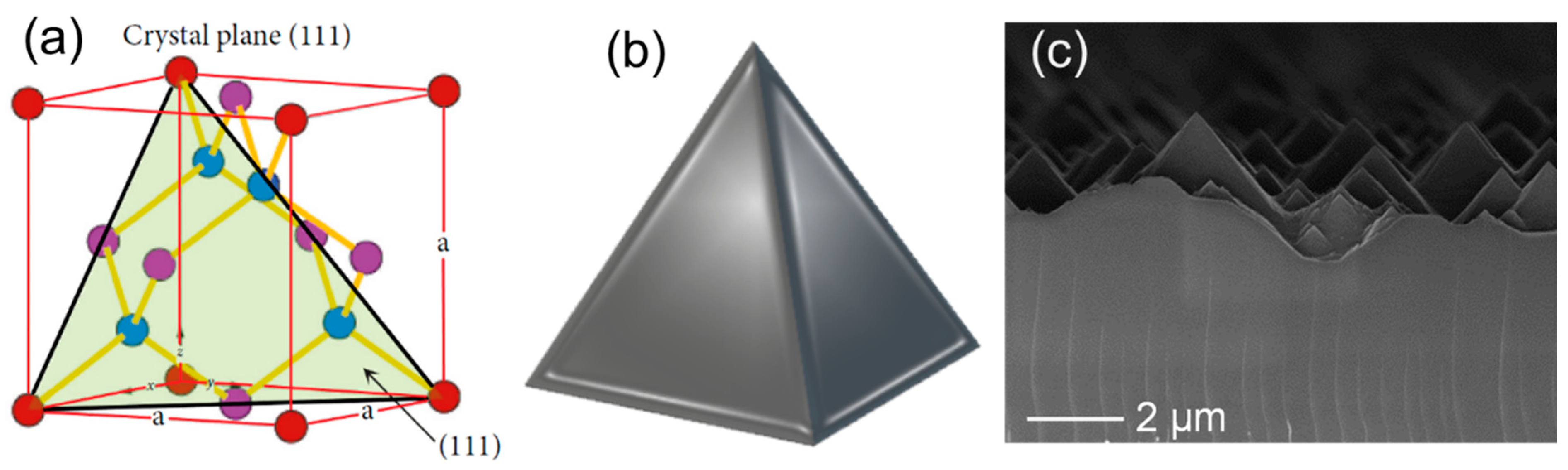
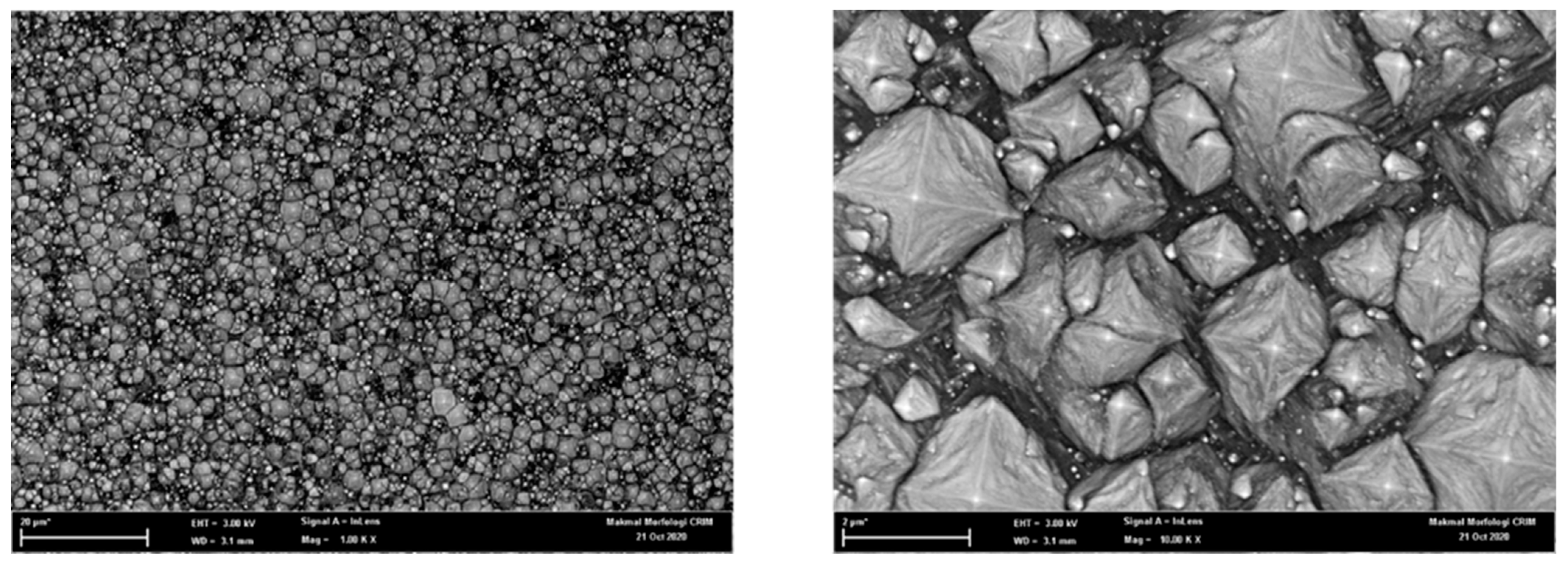
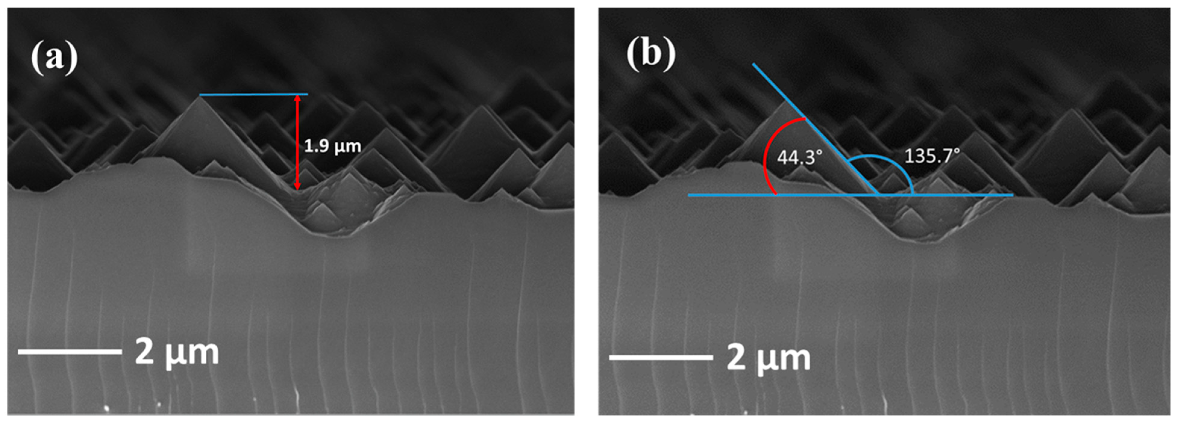
2.1. Silicon Wafer Etching

Currently, one of the most popular techniques for texturing industrial Si solar cells is accomplished through anisotropic etching with IPA and KOH mixed solutions [12]. Typically, upright random-sized micro-pyramidal structures on the mono-crystalline Si(100) surface layer are obtained from this process. In this section, the experimental procedure of the wet chemical anisotropic etching for BSi fabrication is described. The purpose of this experiment is to identify the optimum parameters; (etching solution concentration, etching time, and temperature) required to form the micro-pyramidal structures on the BSi solar cell. P-type mono-crystalline Si(100) wafer (thickness: 300±10 μm, resistivity: 0.01–0.02 ohm-cm) with a size of 2 × 2 cm2 was used throughout the experiment. The Si(100) wafer was initially cleaned through the RCA-1 and RCA-2 processes to remove the organic residues and metal ions from the surface. The process was then followed by the hydrophilic treatment by creating a mixture of Hydrofluoric (HF) acid and deionized water with a ratio of 1:50. After the hydrophilic treatment of the Si(100) wafer, the wet chemical anisotropic etching with Isopropyl Alcohol (IPA) and Potassium Hydroxide (KOH) was conducted. Consequently, KOH pallets were used in the etching solution with 3 various quantities (1, 3, and 5 g), and the IPA solution was altered (5, 7, and 10 mL), accordingly. Meanwhile, the amount of deionized water remained constant (125 mL). Subsequently, the samples were kept in the solution for multiple etching times ranging over 10 to 30 minutes, and the temperature of the solution was controlled to be around 75 ± 5 °C. After the etching process with the alkaline solution, the samples were kept in a mixed solution of Hydrogen Peroxide (H2O2), HF and deionized water at room temperature for 15 min.

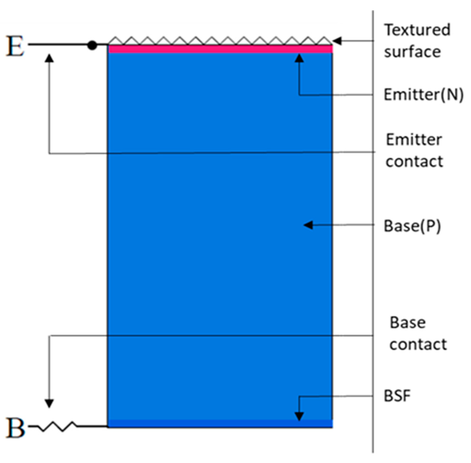
2.2. Solar Cell Modelling

A computer simulation model was employed to utilize the experimental results to interpret and optimize the optical parameters for achieving higher efficiency BSi solar cells. As such, the experimental results related to silicon wafer properties were implemented as input parameters in the simulation. The input parameters were then adjusted accordingly to achieve optimum results. The purpose of the simulation is to elucidate the effect of the experimental procedure optimization to construct an efficient BSi solar cell. PC1D (Personal Computer One Dimensional) is a numerical simulation software, which is one of the most widely used methods to study the electrical and optical parameters of Si solar cells. It was developed at the University of New South Wales in Sydney, Australia. PC1D has been chosen here as it allows simulating the behavior of solar cells based on the simplest structure that is highly accurate and user-friendly. In this study, the software version PC1Dmod 6.2 was used [13].
The schematic model structure and base parameters of the simulated Si solar cell in PC1D software are shown in Figure 1 and Table 1, respectively.

3. Results and Analysis

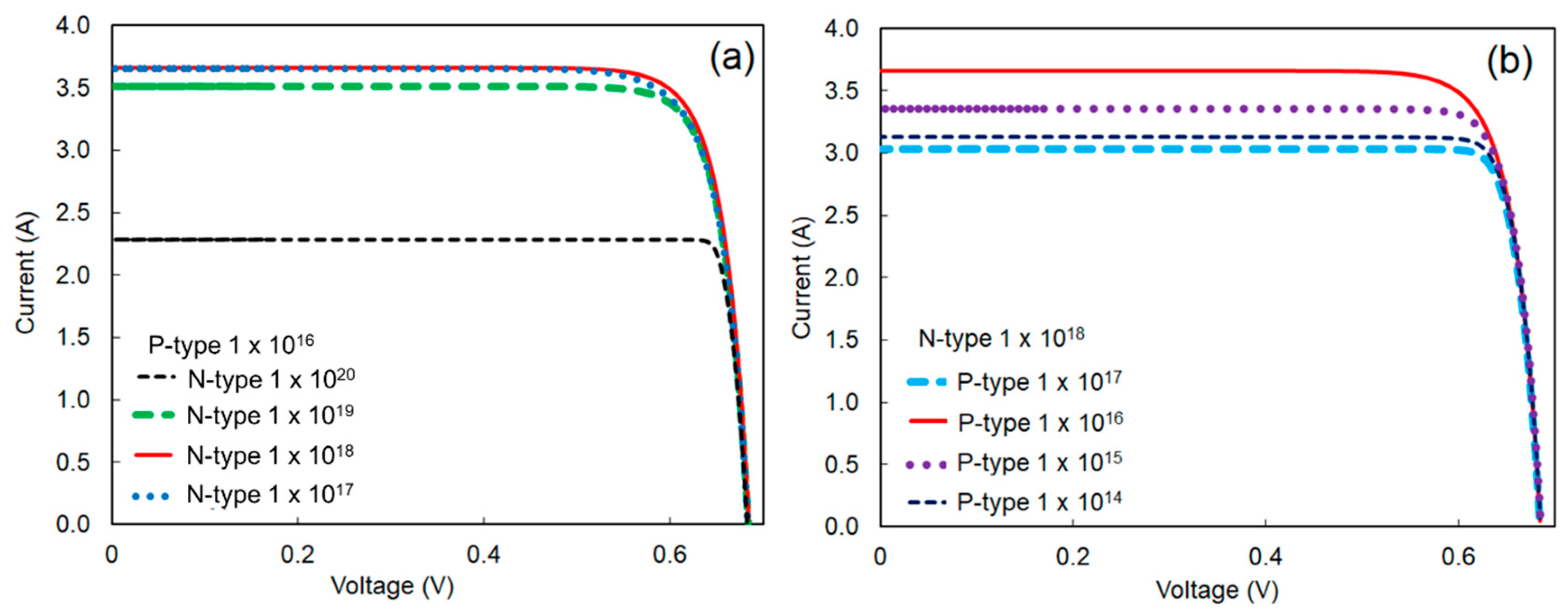
3.1. Optimization of Doping Concentration

Optimization of the doping concentration is an important step to obtain the required doping level for constructing an efficient solar cell. Several combinations of doping concentrations in p-type and n-type were tested in the simulation. The result from different doping concentrations such as short circuit current (Isc), open-circuit voltage (Voc), maximum power (Pmax), fill factor (FF) and efficiency are tabulated in Table 2; as well, I-V characteristics are shown in Figure 2. It can be seen that the doping concentration with the combination of p-type and n-type emitter 1 × 1016 cm−3, and 1 × 1018 cm−3, respectively, show the best efficiency of 19.66% with FF of 84.74%.
Moreover, by observing the levels of doping concentration in Table 2 and the I-V curve in Figure 2, it can be said that enhancing the level of doping concentration does not always increase efficiency. It was recognized that excessive levels of dopant in p-type base and n-type emitter caused the efficiency to drastically reduce. This is because excessive levels of doping concentration can increase the carrier recombination rates, and as a result, reduce the lifetime of minority carriers as well as decrease the minority carrier diffusion length [14]. It should be noted that with the doping concentration for the p-type Si wafer at 1 × 1016 cm−3 and the n-type emitter at 1 × 1021 cm−3, the simulation resulted in an error as transient convergence failure reached the limit. This is probably because the software PC1D cannot give results for convergences that may occur corresponding to non-linearity or time step issues [15].

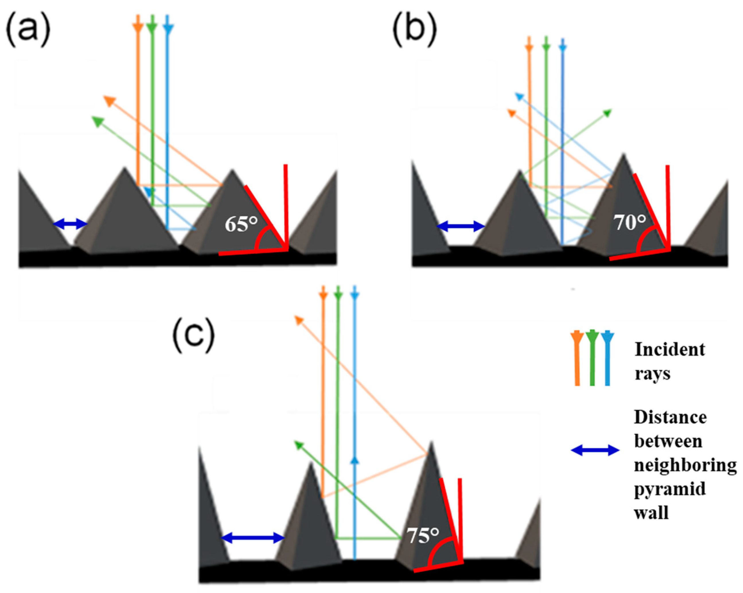
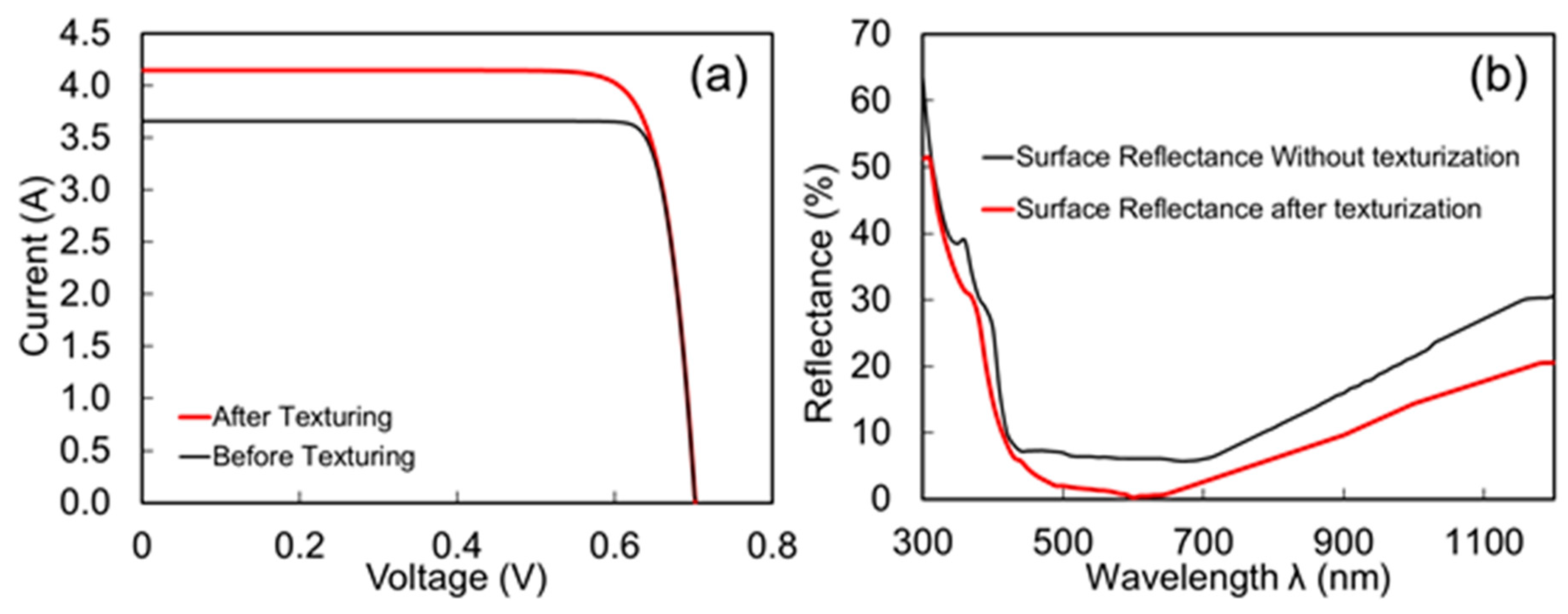
3.2. Impact of Texturization

Structurally, it is important to note that every Si atom of the mono-crystalline Si {100} plane surface contains two dangling bonds as well as two back bonds. The alkaline etchant produces sufficient energy during the etching reaction to break down those dangling bonds [16]. As a result of this breakdown effect, the reaction starts towards the direction of the [100] plane and ends at [111] plane surface-direction. Figure 3a shows that, in the crystal plane structure of {111}, the electrons have one dangling bond and 3 back bonds. These three back bonds produce sufficient strength to stabilize the {111} plane surface. Because of this crystallographic lattice surface structure, the Si {111} plane holds more activation energy compared to the Si {100} plane, and thus, the alkaline etchant is unable to etch along the [111] plane. That is why the etching rate of the alkaline etchant solution on the Si {111} planner surface becomes effectively zero, which helps to form the micro-pyramidal structures [17], as seen in Figure 3b. The cross-section FESEM image of the micro-pyramidal structures obtained in this study via the wet chemical anisotropic etching can be observed in Figure 3c.
For a better understanding of the texturization effects on the BSi solar cell, the simulation was conducted with the wet chemical anisotropic etched sample. Figure 4 depicts the surface morphology of a sample as an example prepared using a KOH: IPA: H2O (1 g: 7 mL: 125 mL) etching solution and a 20-min etching time at 75 °C. Compared to the other experimented parameters, using KOH:IPA:H2O (1 g: 7 mL: 125 mL) provided the best homogenous textured structure that is visually noticeable. As such, the above-mentioned sample was selected for characterization that is discussed in the following sections.
Micro-sys is a free tool to calculate angle and corner, which can specify an angle by using a point on each ray and the vertex. Meanwhile, MB-Ruler is a free tool to measure distances. In this regard, both Micro-sys and MB-Ruler were used to identify the length and the angle of the textured upright pyramid surface obtained from the experimental procedure. By using these tools, we figured out from the experimental data that the size of the upright pyramid structure varied around 1–2 μm as shown in Figure 5a. The base angle of faces of the upright micro-pyramid structures is calculated as 180° − 135.7° = 44.3°. Therefore, 44.3° has been taken as the average angle as shown in Figure 5b. This micro-pyramid height and angle value resulted in an efficiency of 21.93%. Subsequently, for analytical comparison, different values of texturing height and angle were used to identify the optimized solar cell texturization result.
The simulation results of the texturization with the most effective doping layer concentration are presented in Table 3. It can be seen from Table 3 that the micro-pyramidal structures within the height of 1–2 µm standing with a 70° base angle of faces gave the maximum efficiency result of 22.04% with FF 83.22%. The efficiency showed an increasing trend when the lateral angle is enhanced from 44.3° up to 70°. This is because each pyramid forces the reflected rays to be incident on the neighboring pyramids and therefore resulted in several reflections on the pyramid walls as shown in Figure 6. This resulted in an increasing amount of light absorption which occurred due to the surface reflections of the incident rays. However, it was also observed that when the angle reached 75° the efficiency started to decrease.
The reason behind the efficiency reduction when the angle is more than 75° is still unclear. However, it can be said that, since the micro-pyramidal structures play a significant role in determining the extent of reflection for each incident ray, the shapes and angles of the pyramids affect the efficiency of the total solar cell. The illustration in Figure 6 shows that when the pyramid angles are not more than 70° the pyramid shapes are wide enough to reflect the incident rays multiple times. However, when the angles are increased up to approximately 70°, the pyramid shapes are relatively taller with a smaller base, causing the incident rays to be reflected several times and to be ‘trapped’ between the pyramids, therefore increasing the chances to be absorbed. On the other hand, when the angles are 75° and more, the pyramids become too narrow, causing some of the incident rays not to be reflected on the neighbouring pyramid’s wall, resulting in less efficiency. Figure 7a represents the I-V curve for the optimized doping concentration level of the p-type wafer and n-type emitter before and after the texturization process, which shows the significance of texturization to increase efficiency. Figure 7b represents the reflectivity around the 300–1200 nm wavelength band. It was observed that after texturization, the reflectance was significantly reduced, and it reached the lowest point at around 600 nm.

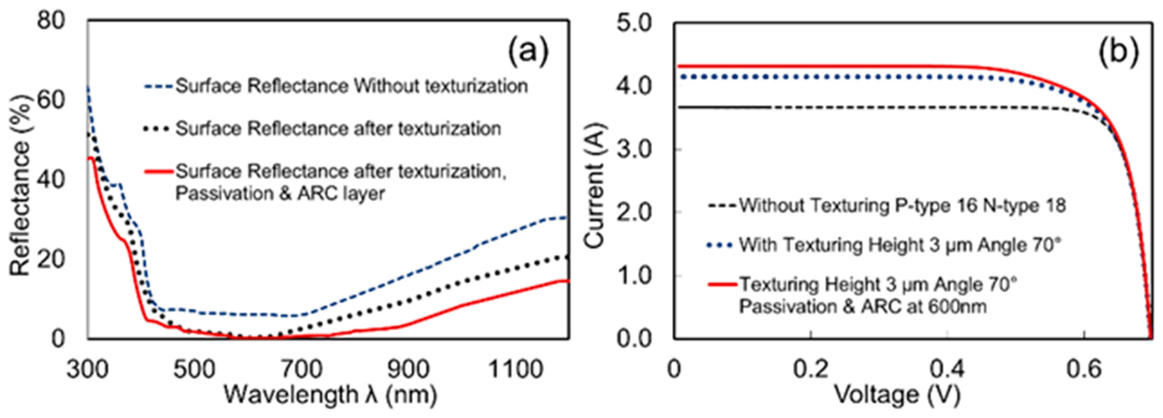
3.3. Effects of Passivation and ARC Layer

Surface passivation, which typically reduces the dangling bond, is an essential part of Si-based solar cells for achieving higher efficiency. Particularly, thermal oxide technology is used to create a very thin SiO2 passivation layer during the fabrication procedure, which is considered as one of the most popular and regular selections for surface passivation [18]. Moreover, Silicon nitride (Si3N4) is also commonly used as the anti-reflection coating (ARC) layer during the fabrication. The ARC layer of Si3N4 is placed upon SiO2 in practical application in which both materials act like two layers of ARC in terms of thickness, refractive index, and the resulting reflectivity. It should be noted that the refractive index of any material is dependent on the wavelength of incident photon or light, thus to realize the optimum thickness for a specific light wavelength in which surface reflectivity of the solar cell will be lowest for that specific wavelength, the following equation was used [19,20,21]:
Refractive   Index ,   η AR = η a × η c ( λ 0 )
Thickness ,   d = λ 0 4 × η AR
where η C = refractive index of the passivation layer and ARC coating for a specific wavelength ( λ 0 ). ηa = refractive index of air, λ 0 = wavelength.
From Equation (1), the refractive index can be calculated for both passivation and ARC layers. By implementing Equation (2), the thicknesses and refractive index values of SiO2 and Si3N4 were estimated for specific wavelengths from references [20,21], as shown in Table 4. The previously obtained optimum values for the doping concentration of the p-type wafer and n-type emitter along with the best-achieved texturization values were kept constant in this part of the simulation. The performance parameters of the BSi solar cell found from the simulation using the refractive index and corresponding thickness of the ARC layers are presented in Table 4.
From Table 4, the best efficiency of 23.14% was achieved with the combination of SiO2 for the passivation layer and Si3N4 for the ARC layer, with a thickness of around 100 nm for SiO2 and 75 nm for Si3N4. These optimum thickness values for both passivation and ARC layers were found at 600 nm of wavelength. It can also be observed from the reflectance results in Figure 8a, the curve with the passivation and ARC layer provided the least amount of reflectance throughout the 300–1200 nm wavelength. Earlier reflectance results showed an increase in reflectance at the beginning of the wavelength at around 300 nm, however, with the combination of a textured surface with the passivation and ARC layer, there is a significant improvement in terms of reducing the reflectance. A common point of reduction at around 600 nm wavelength can also be observed from the reflectance curves in Figure 8a. Overall, the reason behind the reduction of the reflectivity is because of the construction of the two surface layers on top of the textured Si wafer, which assists to trap the light further and thus increases the efficiency of the BSi solar cell. In Figure 8b, three I-V curves (without texturization, with texturization, and texturization with passivation and ARC layer) are represented to compare their efficiency.

4. Conclusions

The study proposes a novel approach to obtain a highly efficient Black Si (BSi) solar cell with alkaline wet chemical etching (KOH:IPA) for industrial application. Hence, surface properties of chemically etched Si wafers were first experimentally investigated to figure out parametric optimization in PC1D numerical simulation targeting high efficiency BSi solar cells. Mono-crystalline Si (100) wafers were etched by KOH:IPA solution to form micro-pyramidal structures on the surface. The optimized feasible threshold values of doping concentration, optimum pyramidal structure’s height and angle have helped to derive properties of anti-reflection-coating (ARC), passivation layer along with the refractive index in simulation. Consequently, the doping concentrations of the p-type wafer and n-type emitter, found during the experimental procedure to be 1 × 1016 cm−3 and 1 × 1018 cm−3, respectively, can be considered as the optimum values to achieve conversion efficiency as high as 19.66%. It was also found that the angle of the pyramidal structures as formed during the etching can be increased to the optimum angle of around 70° to achieve conversion efficiency as high as 22.04%. Furthermore, it was found that upon applying 101.5 nm thickness of SiO2 as the passivation layer and 74.4 nm thickness of Si3N4 as the ARC layer with optimized values of refractive index of 1.48 and 2.015, respectively, conversion efficiency can be further increased to the highest value of 23.14%. Therefore, it can be concluded that all the above chronological studies helped to identify the optimum values for a single layer of Si3N4 and SiO2 for ARC and passivation layers, respectively, on the textured surface to fabricate high efficiency BSi solar cells for cost-effective mass industrial production.

Author Contributions

The experiments were planned and carried out by M.Y.A. and M.A.I., M.Y.A. led the manuscript writing effort, with support from M.A.I. and N.A., A.W.B.M., F.A., T.S.K. contributed to the interpretation of the results and helped to carry out the experiments. N.A. has supervised the research. The findings were discussed by all contributors, and they all contributed to the final manuscript. All authors have read and agreed to the published version of the manuscript.

Funding

The authors received no financial support for the research, authorship, and/or publication of this article.

Institutional Review Board Statement

Not applicable.

Informed Consent Statement

Not applicable.

Data Availability Statement

Data is available from the authors upon request.

Acknowledgments

The authors wish to thank the Ministry of Higher Education of Malaysia (MOHE) for providing the research grant with the code of FRGS/1/2018/STG07/UNITEN/01/3 to support this research. The authors also acknowledge the publication support from the iRMC of Universiti Tenaga Nasional (UNITEN).

Conflicts of Interest

The authors declare no conflict of interest.

References

  1. Liu, X.; Coxon, P.R.; Peters, M.; Hoex, B.; Cole, J.M.; Fray, D.J. Black silicon: Fabrication methods, properties and solar energy applications. Energy Environ. Sci. 2014, 7, 3223–3263. [Google Scholar] [CrossRef] [Green Version]
  2. Pranaitis, M.; Jaraminė, L.; Čyras, V.; Selskis, A.; Galdikas, A. Antireflective structures on silicon sur-face using catalytic nickel nanoparticles. J. Appl. Phys. 2013, 114, 163523. [Google Scholar] [CrossRef]
  3. Hsu, C.H.; Wu, J.R.; Lu, Y.T.; Flood, D.J.; Barron, A.R.; Chen, L.C. Fabrication and characteristics of black silicon for solar cell applications: An overview. Mater. Sci. Semicond. Process. 2014, 25, 2–17. [Google Scholar] [CrossRef]
  4. Huo, C.; Wang, J.; Fu, H.; Li, X.; Yang, Y.; Wang, H.; Mateen, A.; Farid, G.; Peng, K.Q. Metal-Assisted Chemical Etching of Silicon in Oxidizing HF Solutions: Origin, Mechanism, Development, and Black Silicon Solar Cell Application. Adv. Funct. Mater. 2020, 30, 2005744. [Google Scholar] [CrossRef]
  5. Abdur-Rahman, E.; Alghoraibi, I.; Alkurdi, H. Effect of isopropyl alcohol concentration and etching time on wet chemical anisotropic etching of low-resistivity crystalline silicon wafer. Int. J. Anal. Chem. 2017, 2017, 7542870. [Google Scholar] [CrossRef] [PubMed]
  6. Nguyen, V.T.H.; Jensen, F.; Hübner, J.; Leussink, P.; Jansen, H. On the formation of black silicon in SF6-O2 plasma: The clear, oxidize, remove, and etch (CORE) sequence and black silicon on demand. J. Vac. Sci. A Vac. Surf. Film. 2020, 38, 043004. [Google Scholar] [CrossRef]
  7. Atteia, F.; Le Rouzo, J.; Denaix, L.; Duché, D.; Berginc, G.; Simon, J.J.; Escoubas, L. Morphologies and optical properties of black silicon by room temperature reactive ion etching. Mater. Res. Bull. 2020, 131, 110973. [Google Scholar] [CrossRef]
  8. Ding, J.; Zou, S.; Choi, J.; Cui, J.; Yuan, D.; Sun, H.; Wu, C.; Zhu, J.; Ye, X.; Su, X. A laser texturing study on multi-crystalline silicon solar cells. Sol. Energy Mater. Sol. Cells 2020, 214, 110587. [Google Scholar] [CrossRef]
  9. Ou, W.Y.; Zhang, Y.; Li, H.L.; Zhao, L.; Zhou, C.L.; Diao, H.W.; Liu, M.; Lu, W.M.; Zhang, J.; Wang, W.J. Effects of IPA on texturing process for mono-crystalline silicon solar cell in TMAH solution. Mater. Sci. Forum 2011, 685, 31–37. [Google Scholar] [CrossRef]
  10. Mandong, A.M.; Abdullah, Ü.Z.Ü.M. Analysis of Silicon Solar Cell Device Parameters using PC1D. Sak. Üniv. Fen Bilimleri Enst. Derg. 2019, 23, 1190–1197. [Google Scholar]
  11. Plentz, J.; Andrä, G.; Pliewischkies, T.; Brückner, U.; Eisenhawer, B.; Falk, F. Amorphous silicon thin-film solar cells on glass fiber textiles. Mater. Sci. Eng. B 2016, 204, 34–37. [Google Scholar] [CrossRef]
  12. Baker-Finch, S.C.; McIntosh, K.R.; Terry, M.L. Isotextured silicon solar cell analysis and modeling 1: Optics. IEEE J. Photovolt. 2012, 2, 457–464. [Google Scholar] [CrossRef]
  13. Haug, H.; Greulich, J. PC1Dmod 6.2–Improved simulation of c-Si devices with updates on device physics and user interface. Energy Procedia 2016, 92, 60–68. [Google Scholar] [CrossRef]
  14. Brendel, R. Thin-Film Crystalline Silicon Solar Cells; Wiley-VCH Verlag GmbH & Co. KGaA: Weinheim, Germany, 2009. [Google Scholar]
  15. Hashmi, G.; Akand, A.R.; Hoq, M.; Rahman, H. Study of the enhancement of the efficiency of the monocrystalline silicon solar cell by optimizing effective parameters using PC1D simulation. Silicon 2018, 10, 1653–1660. [Google Scholar] [CrossRef]
  16. Seidel, H.; Csepregi, L.; Heuberger, A.; Baumgärtel, H. Anisotropic etching of crystalline silicon in alkaline solutions: I. Orientation dependence and behavior of passivation layers. J. Electrochem. Soc. 1990, 137, 3612. [Google Scholar] [CrossRef]
  17. Chen, W.; Liu, Y.; Yang, L.; Wu, J.; Chen, Q.; Zhao, Y.; Wang, Y.; Du, X. Difference in anisotropic etching characteristics of alkaline and copper based acid solutions for single-crystalline Si. Sci. Rep. 2018, 8, 1–8. [Google Scholar] [CrossRef] [PubMed]
  18. Glunz, S.W.; Feldmann, F. SiO2 surface passivation layers–A key technology for silicon solar cells. Solar Energy Mater. Sol. Cells 2018, 185, 260–269. [Google Scholar] [CrossRef]
  19. Luque, A.; Sala, G.; Palz, W.; dos Santos, G.; Helm, P. Tenth EC Photovoltaic Solar Energy Conference. In Proceedings of the International Conference, Lisbon, Portugal, 8–12 April 1991. [Google Scholar]
  20. Refractiveindex.info. 2021. Refractive Index of SiO2 (Silicon Dioxide, Silica, Quartz)—Gao. Available online: https://refractiveindex.info/?shelf=main&book=SiO2&page=Gao (accessed on 24 February 2021).
  21. Refractiveindex.info. 2021. Refractive Index of Si3N4 (Silicon Nitride)—Philipp. Available online: https://refractiveindex.info/?shelf=main&book=Si3N4&page=Philipp (accessed on 26 February 2021).
Figure 1. Schematic model of Si solar cell.
Crystals 11 00881 g001
Figure 2. I-V curves for different doping concentrations in the emitter (N) and base (P) regions, (a) is for fixed P-type doping with various N-type doping and (b) is for fixed N-type doping with various P-type doping.
Crystals 11 00881 g002
Figure 3. (a) Crystal plane {111}, (b) 3d schematic view of an upright pyramid, (c) cross-section FESEM image of the etched sample.
Crystals 11 00881 g003
Figure 4. FESEM images of wet chemical anisotropic etching with KOH and IPA solution for 20 min at 75 °C temperature.
Crystals 11 00881 g004
Figure 5. (a) The height and (b) the angle of the upright micro-pyramid structure as observed on silicon surface.
Crystals 11 00881 g005
Figure 6. Possible reflection paths of normally incident rays on the micro-structured pyramidal surface of (a) 65°, (b) 70° and (c) 75° base angle of faces. Distance between neighbouring pyramidal walls increases as the angle increased.
Crystals 11 00881 g006
Figure 7. (a) Comparing I-V curve before and after texturing, and (b) reflectance curve before and after texturization.
Crystals 11 00881 g007
Figure 8. (a) Solar cell reflectance of non-textured, textured and textured with passivation and ARC layer, and (b) solar cell I-V curves of non-textured, textured, and textured with passivation and ARC layer.
Crystals 11 00881 g008
Table 1. Base parameters for the simulation.
ParametersValues [Unit]
Device area4 cm2
Emitter contact resistance1.5 × 10−3 Ω
Base contact resistance1.5 x 10−3 Ω
Thickness300 μm
Dielectric constant11.9
Rear diffusion (P)1 × 1020 cm−3
Bulk recombination (lifetime)τn = τp= 250 μs
Front-surface recombination velocity 100,000 cm s−1
Rear-surface recombination velocity118.42 cm s−1
Constant intensity0.1W cm−2
SpectrumAM 1.5G
Table 2. Performance characteristics of the modeled solar cells for different doping concentrations in the emitter (N) and base (P).
Absorber Doping Concentration [cm−3]Emitter Doping Concentration [cm−3]Short Circuit Current (Isc) [A]Open Circuit Voltage (Voc) [V]Max Power (Pmax) [W]Fill Factor (FF) [%]Efficiency [%]
1 × 10141 × 10183.1330.70131.84884.0816.80
1 × 10151 × 10183.3570.70281.98684.1718.05
1 × 10193.224 0.6869 1.841 83.12 16.73
1 × 10202.097 0.6575 1.138 82.53 10.34
1 × 10161 × 10172.083 0.6770 2.083 84.23 18.94
1 × 10183.661 0.6971 2.163 84.74 19.66
1 × 10193.515 0.6843 2.030 84.37 18.45
1 × 10202.284 0.6571 1.258 83.82 11.44
1 × 10²¹Transient convergence failure
1 × 10171 × 10183.032 0.6914 1.759 83.9115.99
Table 3. Data of BSi with various texturing angle.
Texturing Doping Concentration
[cm−3]
Short Circuit Current (Isc) [A]Open Circuit Voltage (Voc) [V]Max Power (Pmax) [W]Fill Factor (FF) [%]Efficiency
[%]
Height
[cm−3]
Angle
1–2 µm44.3°P-type:
1 × 10¹⁶
N-type (Emitter):
1 × 10¹⁸
4.0980.70572.41283.4021.93
54.74°4.1140.70502.41883.3621.98
60°4.1240.70432.42183.3322.01
65°4.1350.70352.42383.2822.03
70°4.1480.70222.42483.2222.04
75°4.1610.70022.42283.1322.02
Table 4. Data of varying SiO2 passivation and Si3N4 ARC layer simulation results (by fixing doping concentration of p-type and n-type emitter to 1 × 1016 cm−3 and 1 × 1018 cm−3 respectively).
PassivationARCTexturing Angle & HeightShort Circuit Current (Isc) [A]Open Circuit Voltage (Voc) [V]Effici-ency
Wave-LengthSiO2 [20]Si3N4 [21][%]
(nm)Refraction IndexThicknessRefraction IndexThickness
(nm)(nm)
2501.523841.0152.281927.389 3.8340.698920.28
3001.50749.7672.166734.614 4.1080.700621.77
4001.489767.1272.072648.248 4.0420.700221.41
5001.481684.3622.034461.443 4.3450.70223.05
6001.4772101.5432.014974.4451–2 µm4.3160.707623.14
7001.4745135.6392.003587.34770°4.1720.70122.11
8001.4727135.8041.9962100.19 4.1310.700721.89
9001.4715152.9051.9913112.991 4.0620.700321.52
10001.4707169.9871.9878125.767 4.020.700121.29
11001.47187.0741.9853138.518 3.9980.699921.17
12001.4696204.1371.9833151.263 3.982699821.08
Publisher’s Note: MDPI stays neutral with regard to jurisdictional claims in published maps and institutional affiliations.

