Article

CVD Elaboration of 3C-SiC on AlN/Si Heterostructures: Structural Trends and Evolution during Growth

1
Université Côte d’Azur, CNRS, CRHEA, Rue Bernard Grégory, 06560 Valbonne, France
2
EASYGaN, SAS, CRHEA/CNRS, Rue Bernard Grégory, 06560 Valbonne, France
3
NOVASiC, Savoie Technolac, Arche Bat 4, BP267, 73375 Le Bourget du Lac, France
*
Author to whom correspondence should be addressed.
Current address: KnowMade SARL, 06902 Sophia Antipolis, France.
Current address: I3S, UMR7271—UNS CNRS, 06900 Sophia Antipolis, France.
Submission received: 13 October 2022 / Revised: 4 November 2022 / Accepted: 5 November 2022 / Published: 10 November 2022
(This article belongs to the Special Issue Feature Papers in Crystal Engineering in 2022)

Abstract

:
(111)-oriented cubic polytypes of silicon carbide (3C-SiC) films were grown by chemical vapor deposition on 2H-AlN(0001)/Si(111) and 2H-AlN(0001)/Si(110) templates. The structural and electrical properties of the films were investigated. For film thicknesses below 300 nm, the 3C-SiC material deposited on 2H-AlN/Si presented a better structural quality than the 3C-SiC films grown directly on Si(111) using the well-established two-step carbonization–epitaxy process. The good lattice match of 3C-SiC with AlN may open a reliable route towards high-quality thin heteroepitaxial 3C-SiC films on a silicon wafer. Nevertheless, the 3C-SiC was featured by the presence of twinned domains and small inclusions of 6H-SiC. The formation of a thin AlSiN film at the AlN/Si interface is also reported. This is the first time such AlSiN layers are described within an AlN/Si heterostructure. Furthermore, noticeable modifications were observed in the AlN film. First, the growth process of SiC on AlN induced a reduction of the dislocation density in the AlN, attesting to the structural healing of AlN with thermal treatment, as already observed for other AlN-based heterostructures with higher-temperature processes. The growth of SiC on AlN also induced a dramatic reduction in the insulating character of the AlN, which could be related to a noticeable cross-doping between the materials.

1. Introduction

The 3C-SiC/AlN heterostructure grown on silicon substrates offers advantages for different fields of investigation, from pseudo-substrate for 2D material growth to research on hybrid material-based microelectromechanical systems (MEMS). It has been attractive in the past decades due to its potential use as a base template for the fabrication of graphene on silicon wafer (GOS) samples [1,2,3,4] because of the presence of oriented 3C-SiC(111), which allows for the formation of high-quality graphene films by thermal treatment. From this perspective, the underlying AlN film, according to its very large bandgap, could permit the electrical insulation of the graphene from the substrate and could be used as a back electrode for transistor fabrication. On the other hand, the 3C-SiC/AlN heterostructure can be a way to obtain high-quality low-thickness (<300 nm) 3C-SiC films for the realization of SiC-suspended membranes or cantilevers for the development of innovative SiC-based MEMS dedicated to aggressive environments [5,6,7,8]. Indeed, from a structural point of view, the very reduced lattice mismatch between 3C-SiC and 2H-AlN (0.9%) suggests the growth of films with a reduced density of defects in comparison to direct growth on silicon substrates (~20% of lattice mismatch), leading to better mechanical properties.
In terms of material elaboration, contrarily to the epitaxy of 3C-SiC on Si and widely documented for decades (see [9] for review) according to the wide availability of silicon substrates, the growth of 3C-SiC on AlN remains weakly described in the literature. In the 1990s, pioneering 3C-SiC growers described some features of 3C-SiC films grown by CVD on AlN/sapphire [10] or AlN/6H-SiC and AlN/Si substrates [11]. These works have demonstrated the first growths of hexagonal and cubic SiC on sapphire and 6H-SiC or silicon, respectively. However, few details have been given concerning the AlN microstructure and the possible interplay between the materials, except for the presence of Al autodoping in SiC during the growth process [10]. The formation of SiC/AlN multilayer heterostructures grown by plasma-assisted gas source of molecular beam epitaxy (MBE) was also reported for growing very thin (<10 nm) quantum well structures [12]. Another work revealed the faulted nature of the films [13]. This study highlighted a possible polytype mixture, favored by the very low energy formation of stacking faults in SiC [14]. We can note that diverse techniques and precursors have been used for the formation of the SiC/AlN heterostructure. For 3C-SiC growth, the chemical vapor deposition (CVD) technique is usually preferred according to various points. Indeed, SiC is grown at higher temperatures than III-nitrides (>1300 °C). This is more easily managed by CVD. Moreover, CVD usually provides higher growth rates than MBE (>1 µm/h). For AlN growth, various techniques can be employed: metalorganic CVD (MOCVD) [10,11,15,16], MBE [17], reactive sputtering [18], or laser-assisted sputtering [19].
From a general point of view, AlN on silicon is a key heterostructure, serving as a nucleation template for the growth of gallium nitride (GaN). For this reason, it has been extensively studied [20]. A general trend is the formation of a columnar structure, irrespective of the growth method. When the growth occurs on Silicon, Si(111) is the most relevant surface orientation according to its three-fold symmetry, matching the six-fold symmetry of AlN(0001). However, Si(110), which has special importance in CMOS technology, was also demonstrated to be an interesting surface for AlN growth [21]. It is worth mentioning that despite very different symmetries and surface atomic arrangements, both Si(111) and Si(110) surfaces lead to the only formation of AlN(0001) films [22]. Although AlN/Si is a well-known system, there is a real lack of information concerning its use as a template for the growth of SiC. Specifically, critical discussion about the influence of the underlying AlN on SiC and the possible modifications of AlN due to SiC growth is, to the best of our knowledge, almost absent from the literature.
Thus, the present work is aimed at contributing to this field by exploring the CVD growth of 3C-SiC on AlN/Si templates. We report noticeable crystalline quality improvement of 3C-SiC with respect to direct growth on a silicon substrate. We also report on some structural modifications undergone by AlN films during SiC growth, as well as the observation of an AlSiN interfacial layer induced by the high temperatures used during the SiC growth process.

2. Experimental Details

2.1. AlN/Si Template Fabrication

For the purpose of the study, several AlN thin films, with thicknesses ranging from 30 to 200 nm, were developed at CNRS-CRHEA on 2-inch on axis and off axis Si(111) and on axis Si(110) substrates. The fabrication was conducted either by ammonia-based molecular beam epitaxy using an Al solid source (NH3-MBE—RIBER Compact 21) at 900 °C, or metalorganic chemical vapor deposition (MOCVD—Close Coupled Showerhead AIXTRON system), with TMAl-NH3 as III-V precursors in a hydrogen atmosphere at 1100 °C and 100 mbar. All AlN thin films are smooth, with a columnar crystalline structure, and grow both the on Si(111) and Si(110) substrates along the [0001] crystalline direction, with Al polarity [22]. For clarity, in the following sections, the growth method of AlN is mentioned only if a noticeable difference was observed between the two techniques.

2.2. 3C-SiC Growth on AlN/Si Templates

The growth of the SiC on the AlN/Si templates was performed using CVD within a resistively heated horizontal homemade system and using silane (SiH4) and propane (C3H8) as precursor gases, diluted in hydrogen as a carrier gas.
In order to prevent any AlN surface degradation, due to hydrogen reactive etching during the thermal ramp-up to the SiC growth temperature [23], this first stage was completed under nitrogen (10 slm). When the growth temperature stabilized, a rapid change in the gas environment, from nitrogen to hydrogen (10 slm), was carried out. After this step, the growth was initiated by introducing silane and propane (from 1 to 5 sccm). The early epitaxial stage was carried out with a C/Si ratio equal to 3, for 90 s, and reduced, subsequently, to unity. The total growth duration varied from 3 to 20 min. The entire process was performed at 800 mbar, and the growth temperature was fixed at 1350 °C. For benchmarking, pieces of 6H-SiC substrates were placed together with the AlN/Si templates in the same runs in order to compare the growth on the AlN under homoepitaxial conditions.

2.3. Characterizations

A set of morphological, structural, and optical characterizations was achieved using scanning electron microscopy (SEM—Supra40 ZEISS), transmission electron microscopy (TEM—JEOL2100F), four circles X-ray diffraction (XRD—Xpert PANALYTICAL), Fourier transform infrared spectroscopy (FTIR—Tensor 27 BRUKER). Electrical I(V) measurements were conducted using a Hg probe (MDC model, central dot with a 0.8 mm diameter). See more details in the Supplementary Material.

3. Results and Discussion

3.1. General Trends Observed in Morphology of 3C-SiC Epilayers

Morphologies and common trends observed on the grown films are, first, reported and discussed.
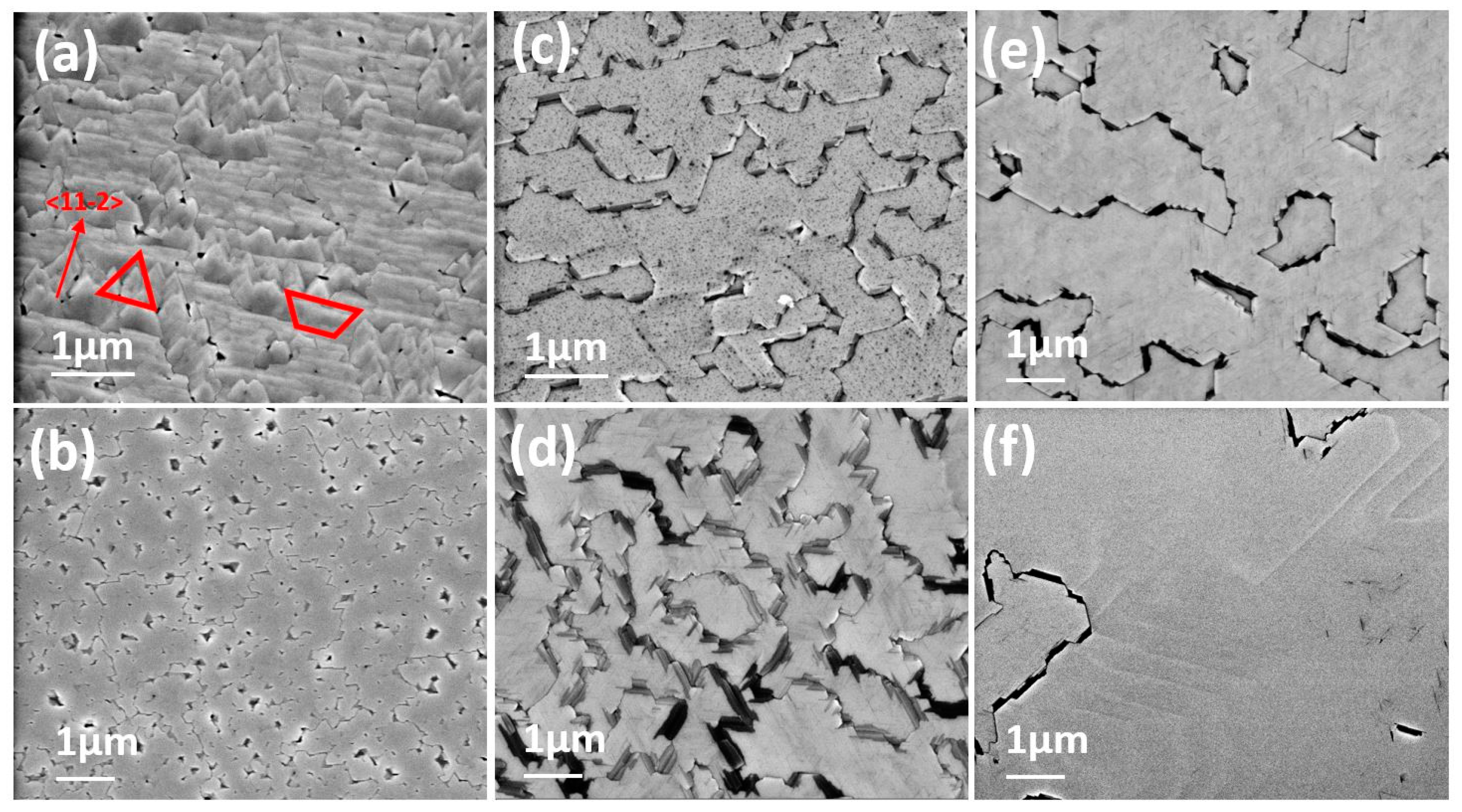
Figure 1 illustrates the morphology obtained on different 3C-SiC/AlN/Si-grown samples. Figure 1a,b shows the morphologies of the 3C-SiC layers obtained after 3 min of SiC growth (i.e., including the C/Si “rich” nucleation followed by a 90 sec and C/Si = 1 growth stage), for MBE AlN/Si(111) 4° off axis and on axis. Similar trends were obtained using the MOCVD AlN/Si templates. The development of triangularly shaped grains, forming either as a stepped structure (Figure 1a) or more randomly distributed with some coalescence defects (Figure 1b), was observed. These differences of morphologies can be attributed to the initial presence of the AlN steps, perpendicular to the Si [1-10] crystalline direction on off axis substrates (see Figure S2 in the Supplementary Material). With a similar growth duration, a comparable quantity of SiC was assumed to form for both cases. We noted that islands developing on the off axis AlN/Si template (Figure 1a) tended to grow on the surface by forming triangles pointing either perpendicularly to the AlN steps or in the opposite direction with a truncated side, as indicated in the figure. This point is discussed thoroughly hereafter, but this is a typical trend observed during the growth of a three-fold symmetry material growing on a six-fold symmetry substrate (twinning mechanism), as in the case of 3C-SiC growth on hexagonal SiC substrates [24,25].
Figure 1c,d shows the morphologies observed on the 3C-SiC/AlN/Si samples with a longer duration of growth (20 min, ~300–320 nm, measured by FTIR). We obtained, for both the off and on axes, a SiC surface presenting some large domains, separated from each other by trenches. The AFM measurements (not shown) allowed us to determine that, on a given visible domain, the roughness was quite low (RMS = 1 nm on a 5 × 5 µm2 scan). On the other hand, the trenches that formed domain boundaries had typical depths in the range of 10–20 nm. According to Figure 1a,b, the observed grains should correspond to some enlarged grown SiC twinned domains. It can be noticed that, for almost equivalent SiC film thickness, the SiC domains appear qualitatively larger on the off axis templates, showing a benefit to using initially misoriented substrates. In addition, Figure 1e shows the morphology obtained on a 320 nm-thick 3C-SiC grown on an on axis AlN/Si(110) template. It presents the same microstructure but with larger twinned domains compared to Figure 1c,d. This opens the question of the underlying AlN influence on SiC growth.
Indeed, if some differences between the on and off axis templates can be attributed to the stepped-like feature of the off axis templates, noticeably larger domains on the AlN/Si(110) were obtained even for non-disoriented substrates. As mentioned before, AlN grows with the same [0001] growth direction, both for Si(111) and Si(110). Nevertheless, it was shown that, according to a favorable lattice match, AlN presented some better structural properties on Si(110) than on Si(111) [22]. This appears interesting to favor the development of large SiC domains.
Furthermore, as mentioned before, some growth processes occurred simultaneously on AlN/Si and 6H-SiC, and the latter was taken as a reference sample for validating the growth process. Figure 1f shows the morphology obtained on such a 6H-SiC substrate. A smooth surface, featured by the development of steps, is clearly visible. The presence of a domain included within a larger one can be noted. This appears to be typical of a 3C-SiC film formed on a 6H-SiC, with small domains included in larger ones, revealing the development of twinned domains [26]. The formation of such a typical 3C-SiC film on a 6H-SiC polytype confirms that the adopted growth conditions were suitable for homoepitaxial growth and validates the chosen C/Si ratios. It can also be noticed that the lateral expansion of a given domain was, by far, larger than those observed on the AlN/Si templates, revealing a possible influence of the underlying AlN film.
Another point of interest relies on the similar morphologies observed both for on axis and off axis samples (Figure 1c,d). According to the difference in morphologies observed for thinner films, different morphologies should have been expected for larger thicknesses. A possible assumption for explaining this can be the possibility of two separated SiC domains growing on the same AlN step with a 180° misorientation from one another, with an equivalent probability (twinning). Therefore, the use of a stepped surface becomes an insufficient condition for removing the twinning mechanism because, as long as some twinned domains merge continuously during the film thickening, no preferential domain orientation becomes dominant. More details about the twinning issue are given in the next sections.
Nevertheless, despite the presence of twinned domains, some interesting features must be underlined. First, the typical sizes of SiC-grown grains are quite large relative to the film thickness. Indeed, although they have irregular shapes, grains can expand laterally over 2 µm along a direction, namely about ten times larger than the thickness. For comparison, in the case of growth of 3C-SiC directly on Si(100)-oriented substrates, epitaxial grains can present two different in-plane epitaxial relations and form antiphase domains differing from each other by a 90° rotation on the (100) growing plane [27]. Thus, domains are separated by boundaries (anti-phase boundaries, APBs) which constitute a morphological defect very similar, in terms of roughness, to the grain boundaries presently observed. For 3C-SiC/Si(100), the lateral expansion of each domain is comparable to the film thickness. Similar observations were made for 3C-SiC/Si(111) [28]. It can be mentioned that the presence of prominent APBs on the surface of the as-grown SiC epilayers can be solved using a chemomechanical polishing (CMP) process which allows for reducing the overall RMS, including APBs, to below one nm [29]. It can be expected that the present observed grain boundary-induced roughness could be reduced in the same way. Other points of interest of the grown 3C-SiC layers rely on their structural properties, as discussed hereafter.

3.2. Structural Investigations

The structural properties of the grown films were investigated using XRD and TEM-HRTEM analysis.
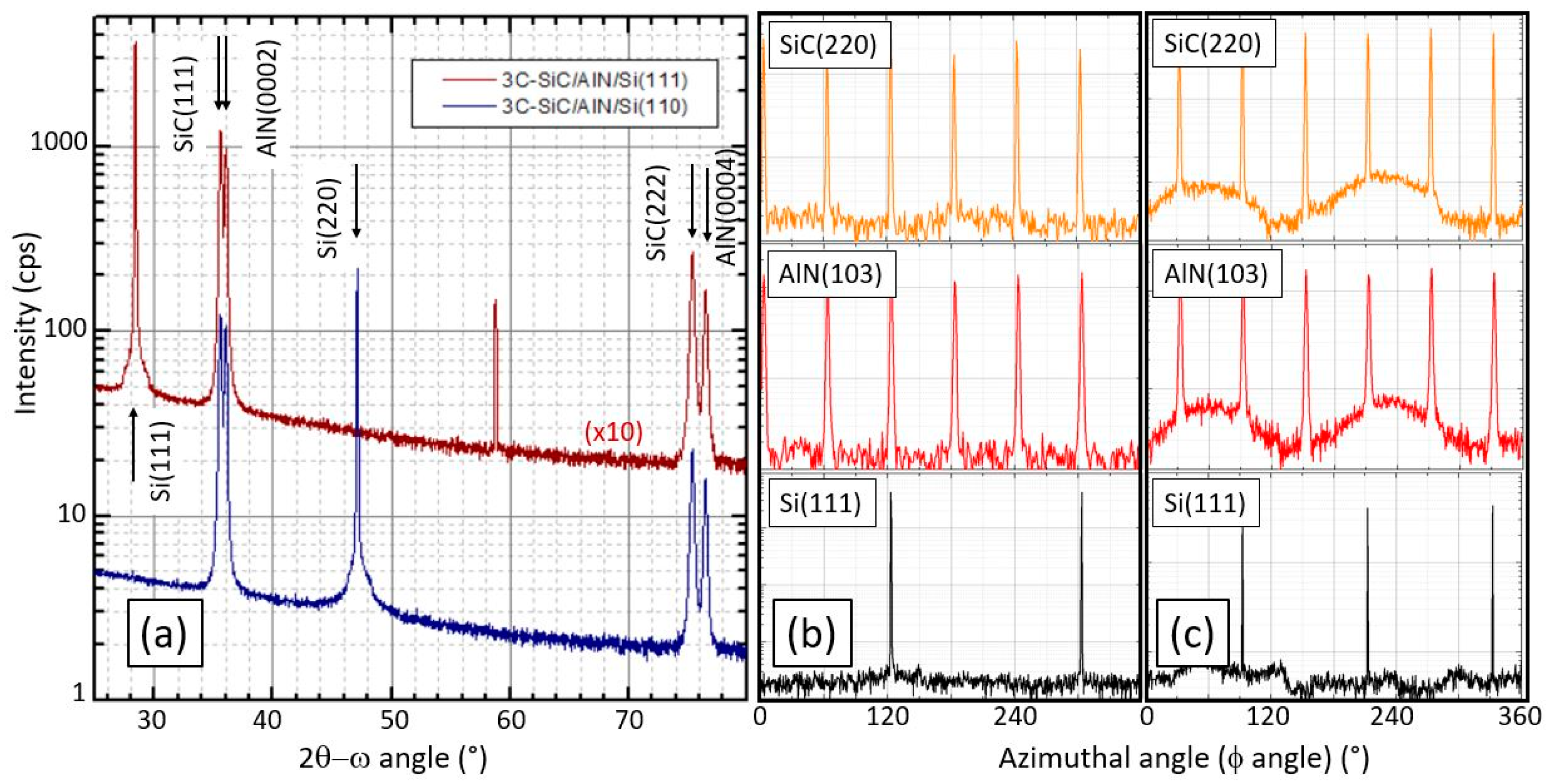
Firstly, the 2θ−ω scans (Figure 1a) confirm that the 3C-SiC films were (111)-oriented, and no other crystalline direction was observed. It must be highlighted that the same orientation was conserved on the AlN films grown either on the Si(111) or Si(110) substrates.
According to the symmetry difference between wurtzite AlN and cubic SiC, the latter is expected to develop twinned domains, as previously mentioned. This twin formation is similar to that encountered during the growth of cubic SiC on hexagonal SiC polytypes [24,25]. The azimuthal scans, recorded along diverse out-of-plane reflections, demonstrate the presence of twinned domains in SiC, as illustrated in Figure 2b,c. Indeed, six peaks, with a 60° spacing, were recorded along the SiC(220) out-of-plane direction, corresponding to the six SiC{220} planes (top spectra in Figure 2b,c), whereas only three, with 120° spacing, were expected in the case of a single-domain SiC(111)-oriented film. This clearly denotes the presence of SiC twinned domains, differing from each other by a 180° rotation and corresponding to the grains observed by SEM in the previous section. From these measurements, the in-plane epitaxial relations of the SiC/AlN heterostructures grown on (i) Si(110) and (ii) Si(111) could be determined, respectively, as follows:
(i)
3C-SiC [0-11]//2H-AlN [11-20]//Si [1-10]
and 3C-SiC[-211]//2H-AlN [1-100]//Si [001]
(ii)
3C-SiC [0-11]//2H-AlN [11-20]//Si [01-1]
and 3C-SiC [-211]//2H-AlN [1-100]//Si [-211]
These epitaxial relationships are similar to those already reported for SiC growth at a low temperature using the PLD technique both for AlN and SiC formation [4] on Si(110) substrates. According to the almost equivalent diffraction intensities of different domains, we can conclude that the statistical occurrence of both domains is equivalent. In the present case, it must be highlighted that the use of off axis AlN/Si(111) templates did not reduce the relative contribution of a given domain (see Figure 2b,c). Our results differ noticeably from those of [4], where a single-domain SiC film was obtained using the off axis AlN/Si(110) substrates. Discrepancies between this observation and our results can be related to the very different growth conditions between our work and those of [4].
In the case of 3C-SiC (three-fold symmetry) growth on hexagonal (4H- or 6H-) SiC substrates (six-fold symmetry), the formation of twinned domains is an issue that sparks an ongoing debate. Some authors have mentioned that twin suppression can be driven by adjusting the growth parameters [25,26]; others reported the need for adequate substrate preparation [30]. For the growth of 3C-SiC on 2H-AlN, many parameters can also influence the initial nucleation of SiC on AlN. As in the case of growth on hexagonal SiC, a step-flow growth mode [31] should favor the occurrence of single-domain SiC. However, our data show that the use of stepped AlN, formed on off axis Si substrates, is insufficient to suppress twinned SiC domains and, in the absence of a step-flow growth mode, these domains can form at two different locations on a given AlN step, as underlined before. Our morphological observations (see Figure 1a) clearly indicate that this is the case with the appearance of a 3D growth mode, favored by our experimental growth conditions.
Nevertheless, the grown SiC films present an attractive feature. Indeed, Figure 3 shows the full width at half-maximum (FWHM) of the SiC(111) symmetric diffraction line as a function of the film thickness. In addition to these values, FWHMs of SiC(111) measured on SiC films grown directly on Si(111) substrates in a lab using the optimized carbonization–epitaxy growth process described in [32] are reported. We noted the very reduced values of the FWHMs for SiC films on AlN were thinner than—300 nm compared to SiC films on Si grown with the carbonization–epitaxy process. For SiC grown on AlN, the FWHMs remained below 2500 arcsec, even for the thinnest films, whereas a very strong broadening of the SiC(111) FWHMs for SiC on Si was observed for thicknesses below 200 nm. This confirms that, according to the very reduced lattice mismatch between SiC and AlN, SiC can grow with a lower density of crystalline defects than on silicon, where the carbonization stage is required and forms, in the early stage of growth, a very defective layer for this range of thickness [9]. This point is particularly important as it shows the ability to obtain a 3C-SiC film of low thickness with crystalline quality is, by far, better than using only Si as the substrate. This should be very beneficial for the design of microelectromechanical structures where the structural properties influence the mechanical properties and, thus, can potentially impact the physical parameter of devices [5,6].
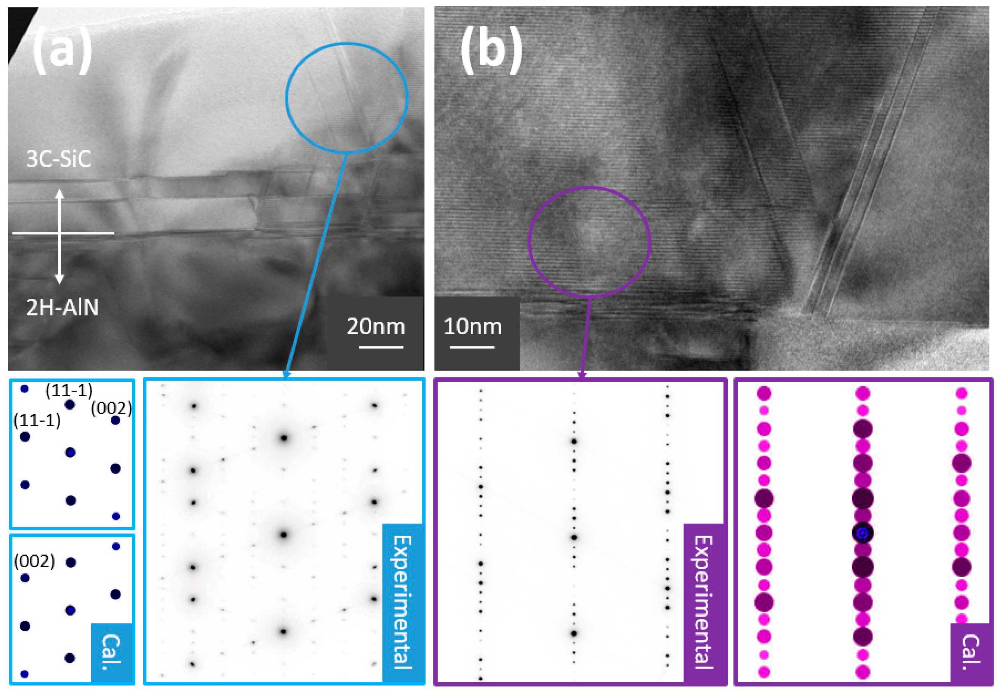
TEM observations allowed us to go a step further in the analysis. Figure 4 shows two TEM cross-section images of the interface between SiC and AlN along the <1-10> SiC zone axis. The large-scale image of Figure 4a allows for observing the presence of numerous stacking faults. The formation of stacking faults is a very likely mechanism in 3C-SiC, according to the very low energy of formation, and it is largely reported during growth on silicon. The presence of twins is also confirmed by the good match between the simulated selected-area electron diffraction (SAED) patterns, obtained by assuming the existence of twinned domains, and experimental ones (see the inset in Figure 4a). Zooming in on the SiC/AlN interface (Figure 4b) reveals that many SiC zones close to the interface presented a hexagonal arrangement, which appeared as a 6H-SiC polytype, as evidenced by their diffraction patterns (inset in Figure 4b). These zones can expand some tens of nm away from the interface.
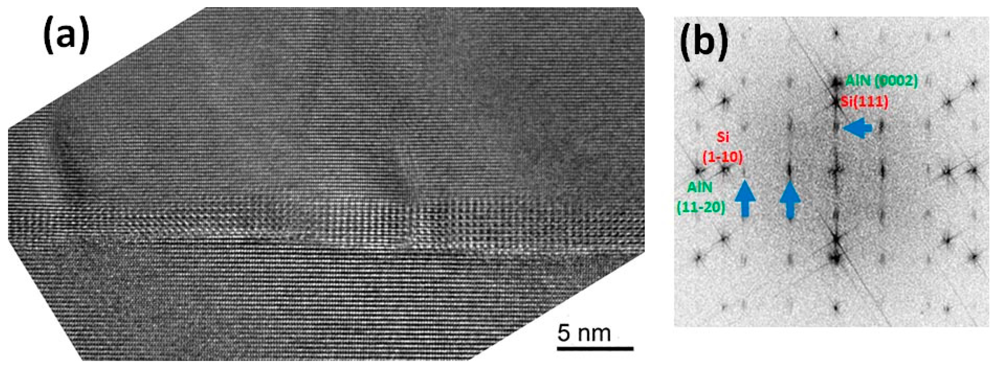
Furthermore, Figure 5 is an HRTEM image of the AlN/SiC interface along a <11-2>Si/<10-10>AlN zone axis, revealing a structural modification occurring after either the SiC growth or simple annealing of the AlN/Si at 1330 °C. A thin (~3–5 nm) layer, adopting a crystalline arrangement that differs from that of wurtzite AlN and Si, was observed. The Fourier transform (FT) of the image (Figure 5b) is the superposition of the Si<11-2> and AlN<1-100> diffraction patterns, plus extra diffraction spots (blue arrows) demonstrating triple in-plane and double out-of-plane periodicities. This is characteristic of the Al5+αSi5+δN12 compound obtained on AlN layers on sapphire by the diffusion of Si at temperatures between 1350 °C and 1550 °C and first observed by some of the present authors [33]. The Si/Al ratio is close to 1 in this alloy, which demonstrates a large AlN/Si interdiffusion process during the SiC growth. To the best of our knowledge, such an AlSiN alloy formation on an AlN/Si heterostructure has never been reported.

3.3. Electrical Behavior and AlN Structural Modifications Induced by Process

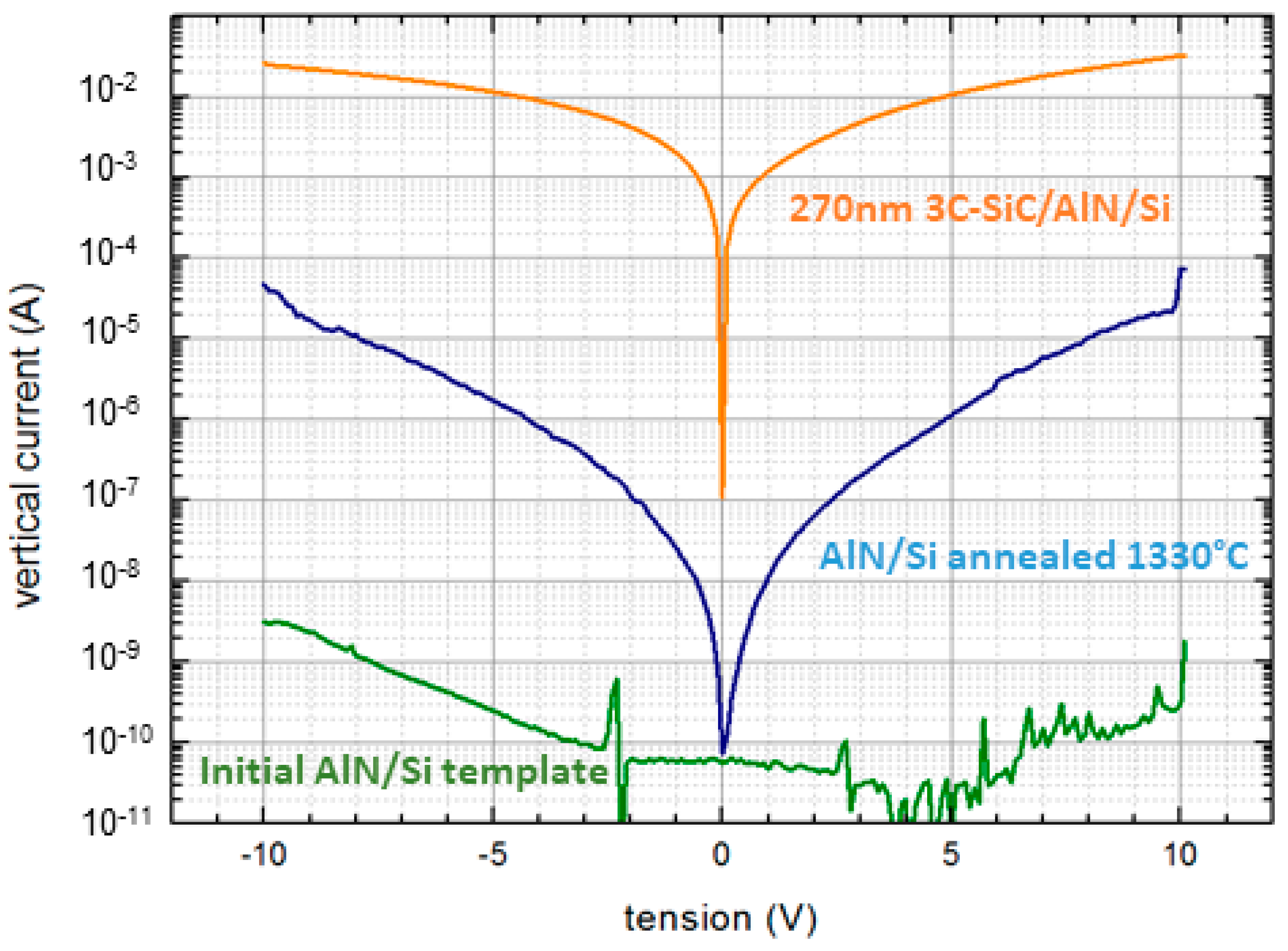
According to the interest in using AlN as an intermediate insulating layer in the SiC/AlN/Si heterostructure, we investigated some electrical-related trends induced by the SiC growth process. At first, an assessment of the electrical behavior was conducted by vertical I(V) measures. Figure 6 reports the measurements made contacting the upper face with a Hg probe and the back of the silicon substrate with a metal chuck: (i) on a 100 nm thick AlN/Si(111)—(p type—1–10 ohm.cm) template before the SiC growth, (ii) on the same AlN/Si template annealed at a temperature similar to that used for growing SiC and (iii) on a 270 nm thick SiC layer on AlN/Si. Similar features were obtained using thicker AlN films or using Si(110) substrates. A very low vertical current was recorded for any voltages for the non-annealed AlN/Si heterostructure, attesting to a very high insulating characteristic of the AlN film despite the presence of structural defects.
After annealing, a significantly higher current was recorded through the AlN/Si heterostructure. This trend was further enhanced when considering the complete 3C-SiC/AlN/Si heterostructure, with an ohmic character of the I(V) characteristics and current values seven orders of magnitude higher than in the case of the initial AlN/Si template, evidencing a vertical current flowing through both SiC and AlN.
The electrical flow through SiC can be expected, according to the electrical activity of inclined stacking faults, clearly visible on the TEM images (Figure 4) [34]. However, the fact that the current could flow vertically across the AlN film is more intriguing, especially regarding its initial insulating character before SiC growth or annealing. This lets us assume that the high-temperature annealing and/or the CVD SiC growth conditions can affect the AlN electrical properties.
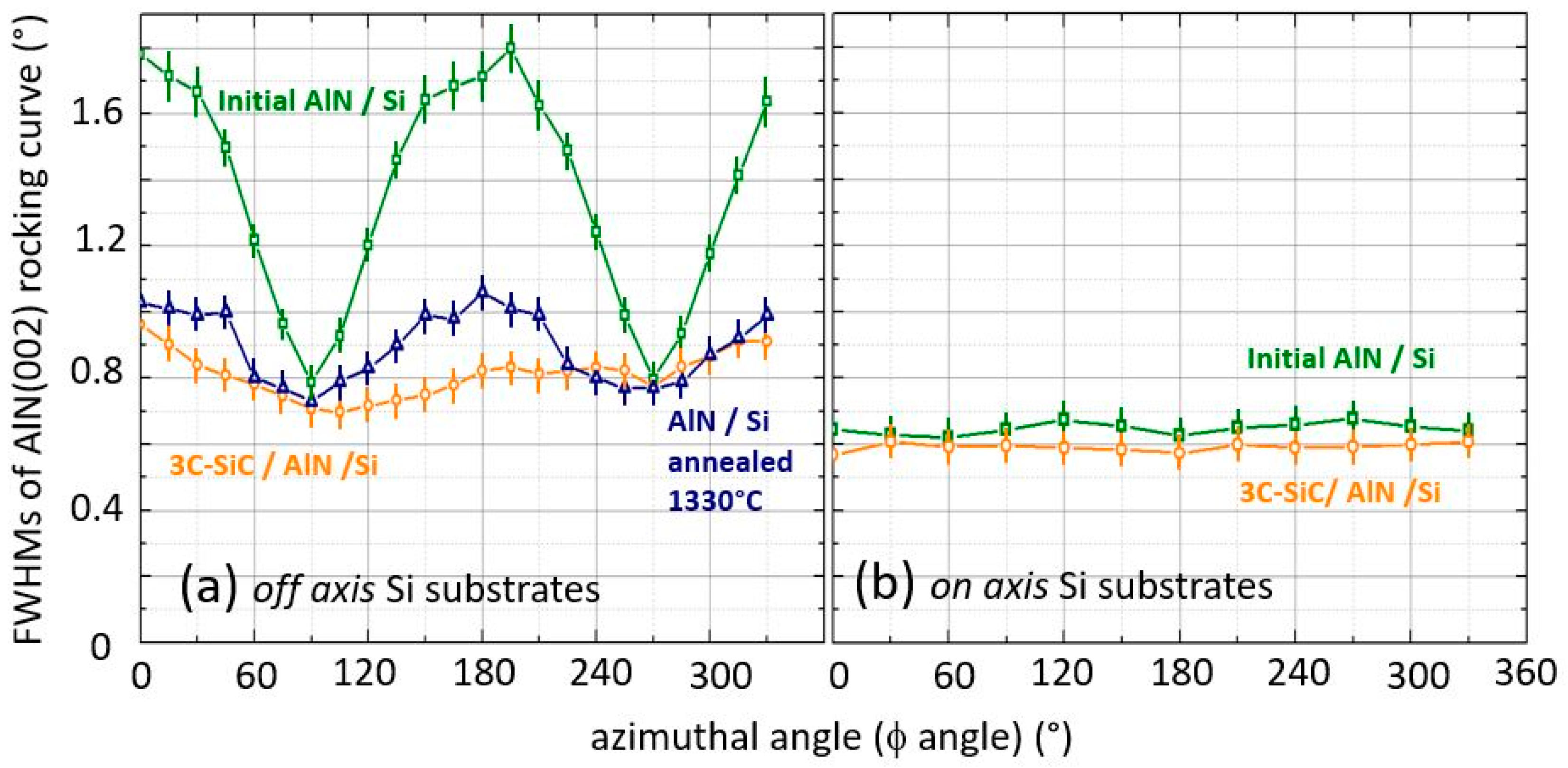
The XRD measurements carried out on these heterostructures are helpful for understanding these trends. Indeed, Figure 7a reports the azimuthal dependence of the FWHMs recorded on an as-grown AlN(50 nm)/Si(111) (4° off axis) heterostructure, as well as the FWHMs recorded after either annealing or the regrowth of SiC on this heterostructure. To be sure of performing relevant comparisons, the initial AlN/Si wafer was sliced into two pieces, each of them being dedicated to a specific treatment—annealing or SiC growth. Figure 7b shows the data recorded on the AlN(100 nm)/Si(111) (on axis), excluding annealing, which was not performed.
For the AlN grown on off axis substrates (Figure 7a), a strong anisotropy of the recorded values, dependent on the azimuthal angle, with two FWHMs maxima separated by 180° and corresponding to the [11,12,13,14,15,16,17,18,19,20] crystalline direction (i.e., the off-cut direction), was observed. The realization of either thermal annealing at 1330 °C or a CVD SiC growth process on such AlN films led to a significant evolution of the FWHMs. This was especially true for the off axis heterostructures (Figure 7a) for which FWHMs were reduced along the crystalline directions previously exhibiting the largest values. We observed that this effect was less pronounced after the simple annealing compared to after the SiC growth process. We also noted that only a slight evolution was observed for the crystalline directions initially presenting the lowest FWHMs ([1-100] and [-1100]). On the other hand, the decrease in the FWHMs was less pronounced (within 10%) in the case of the on axis heterostructures, for both the Si(111) (see Figure 7b) and Si(110) substrates.
Such observations indicate that both thermal annealing and the CVD SiC growth process can influence the structural properties of the underlying AlN. In the case of thermal annealing, only a physical mechanism can be involved (a thermally induced mechanism), whereas, in the case of SiC growth, both physical and chemical mechanisms could be involved, the latter being related to the reactive gas environment used for the growth. Nevertheless, according to the slight differences in behavior observed between thermal annealing and the SiC growth, it seems probable that the chemical effect would be low compared to the thermally induced effect. This is supported by previous works. Indeed, it was shown that the structural properties of AlN films can be greatly modified by performing specific high-temperature annealing [35]. In this work, the authors used sputtered AlN deposited on sapphire templates. The annealing temperatures were in the range of 1600–1700 °C. A reduction of the dislocation density was evidenced as a consequence of the thermal annealing.
In our work, we dealt with a quite different system (AlN with better initial crystalline quality, grown by MOCVD on a silicon substrate) and with lower process temperatures (typically 1100 °C). However, the results in Figure 7 tend to demonstrate that a dislocation healing should have occurred according to the FHWM reduction after annealing and the CVD growth process, with a bit more of a pronounced effect after the CVD SiC growth. Nevertheless, it is not possible to definitely conclude about the specific contribution of the SiC growth stage on dislocation healing. This point remains open for discussion.
It is clear from our work that the temperature conditions were sufficient to modify the AlN microstructure and that the SiC growth conditions induced further modifications, according to the significant increase in the vertical current flow through the entire SiC/AlN/Si heterostructure (see Figure 6). This could be related to the significant cross-doping of AlN with Si or C species during the growth and the reverse case, namely the incorporation of Al or N in SiC during its growth [10,17].
A strong indication for the presence of a cross-doping effect in our experiment is given by the infrared reflectance measured on some 3C-SiC/AlN/Si samples. Figure 8 shows a reflectance spectrum acquired on the SiC(270 nm)/AlN(100 nm)/Si heterostructure. This spectrum shows the typical SiC and AlN TO-phonon-related structures close to 660 and 800 cm−1 [36,37]. These structures were superimposed onto a high continuous background that slowly declines after—1000 cm−1.
FTIR experimental reflectance spectra of materials or stacked heterostructures can be modeled by a classical dielectric model, where reflectance can be calculated from both the definition of the dielectric functions of each material present in the stack and the Fresnel coefficients at each interface [36,38]. The presence of free carriers (and, thus, doping) can significantly affect the reflectance spectrum and can be modeled by introducing a plasmon term (Drude term) to the dielectric function of the material. This Drude term is well separated from the lattice contribution (vibrations), which are described with a Lorentzian term. Thus, a qualitative assessment of a possible cross-doping effect could be carried out by comparing the experimental data with a simple dielectric calculation where we assumed different carrier concentrations. In the present work, a home-made code under a SCILAB environment [39] was used for calculating the dielectric–based reflectance of a 3C-SiC/AlN/Si heterostructure, taking as phonon parameters those reported in the literature [37,38] and considering a plasmon term, both in the SiC and in the AlN layers, as variable parameters, ranging from 200 to 2200 cm−1 for targeting carriers concentrations of 1018, 5 × 10¹⁸, 1019, 5 × 10¹⁹, and 1020 cm−3. In addition to the experimental data, Figure 8 shows the calculated reflectance spectra obtained with these different doping levels. The background, against which the SiC and AlN phonon-related peaks are observed, was soundly enhanced by the introduction of plasmon terms. For obtaining a qualitatively good agreement between the experiment and calculation, a carrier concentration roughly in the mid-1019 cm−3 was required. Obviously, our approach remains a rough estimation, as our model cannot take into account the presence of carrier concentration gradients at the interfaces or inside layers. From an experimental point of view, these gradients are very likely to occur, as cross-doping should generate diffusion mechanisms. At first, the calculated reflectance spectra show trends that support the presence of a noticeable cross-doping effect, at quite a high level, between the SiC and AlN. Further experimental data are required to go further into detail on this point.

4. Conclusions

The study gives an extended overview of the trends and issues encountered during the growth of cubic SiC by propane–silane-assisted CVD on 50–270 nm thick AlN/Si templates. We tried to document typical trends observed on the SiC layer as well as the impact of the process on AlN.
The results show that 3C-SiC grew by developing twinned domains. The use of off axis substrates did not suppress them but tended to result in larger SiC grains. This effect was shown to be more effective on Si(110). However, according to the good lattice match with AlN, the approach allowed for 3C-SiC films to grow soundly, featured by better structural properties than those obtained growing 3C-SiC directly on Si at a thickness below roughly 300 nm.
The effects of the SiC growth process on the AlN structural properties were also investigated. A noticeable structural modification was evidenced and could be related to a dislocation density reduction. The formation of an AlSiN interfacial film between AlN and Si was also demonstrated. In addition, the results show evidence of a strong modification of the electrical behavior of the AlN film due to the growth of SiC. This point could be a severe issue if not fixed for the interest of the 3C-SiC/AlN/Si heterostructures if insulation is required. These trends were observed for the first time in the case of AlN grown on Si. They illustrate the need to consider the impact of high-temperature processes on AlN properties when AlN films are used as templates for the development of heterostructures.
Further developments, especially for tuning the nucleation layer, which is potentially useful for lowering the effect of the high-temperature-induced cross-doping effect, are required and will be conducted. Nevertheless, the ability to grow such thin 3C-SiC/AlN/Si, with good SiC crystalline quality remains interesting for providing new templates for applications for which the electrical issue is not an obstacle.

Supplementary Materials

The following supporting information can be downloaded at: https://0-www-mdpi-com.brum.beds.ac.uk/article/10.3390/cryst12111605/s1, Figure S1: SEM micrograph recorded on AlN/Si(111) on axis. Figure S2: SEM micrograph recorded on AlN/Si(111) 4° off axis. Figure S3: SEM micrograph recorded on AlN/Si(110) on axis.

Author Contributions

M.P.: project supervision, epitaxy, characterization, SEM, FTIR, DRX analysis, and writing; E.F., A.M., S.R., F.S. and L.N.: SiC and AlN epitaxy; A.C.: structural characterizations; M.Z.: SiC epitaxy, analysis and draft review; R.C.: electrical measurements; Y.C.: electrical measurements and draft review; P.V.: TEM analysis and draft review. All authors have read and agreed to the published version of the manuscript.

Funding

This research received no external funding.

Institutional Review Board Statement

Not applicable.

Informed Consent Statement

Not applicable.

Data Availability Statement

The data presented in this study are available within the article.

Conflicts of Interest

The authors declare no conflict of interest.

References

  1. Suemitsu, M.; Fukidome, H. Epitaxial graphene on silicon substrates. J. Phys. D Appl. Phys. 2010, 43, 374012. [Google Scholar] [CrossRef]
  2. Suemitsu, M.; Jiao, S.; Fukidome, H.; Tateno, Y.; Makabe, I.; Nakabayashi, T. Epitaxial graphene formation on 3C-SiC/Si thin films. J. Phys. D Appl. Phys. 2014, 47, 94016. [Google Scholar] [CrossRef]
  3. Hsia, B.; Ferralis, N.; Senesky, D.G.; Pisano, A.P.; Carraro, C.; Maboudian, R. Epitaxial graphene growth on 3C-SiC(111)/AlN(0001)/Si(100). Electrochem. Sol. State Lett. 2011, 14, K13–K15. [Google Scholar] [CrossRef]
  4. Narita, S.; Nara, Y.; Enta, Y.; Nakazawa, H. Growth of 3C-SiC(111) on AlN/off axis Si(110) heterostructure and formation of epitaxial graphene thereon. Jap. J. Appl. Phys. 2019, 58, SIIA16. [Google Scholar] [CrossRef]
  5. Boubekri, R.; Cambril, E.; Couraud, L.; Bernardi, L.; Madouri, A.; Portail, M.; Chassagne, T.; Moisson, C.; Zielinski, M.; Jiao, S.; et al. Electrothermally driven high frequency piezoresistive SiC cantilevers for dynamic atomic force microscopy. J. Appl. Phys. 2014, 116, 054304. [Google Scholar] [CrossRef] [Green Version]
  6. Michaud, J.-F.; Portail, M.; Alquier, D. 3C-SiC—From electronic to MEMS devices. In Advanced Silicon Carbide Devices and Processing; InTechOpen Limited: London, UK, 2015. [Google Scholar] [CrossRef] [Green Version]
  7. Portail, M.; Chenot, S.; Ghorbanzadeh-Bariran, M.; Khazaka, R.; Nguyen, L.; Alquier, D.; Michaud, J.F. Designing SiC based CMUT structure: An original approach and related material issues. Mat. Sci. Forum 2022, 1062, 94–98. [Google Scholar] [CrossRef]
  8. Shanmugam, P.; Iglesias, L.; Portail, M.; Dufour, I.; Certon, D.; Alquier, D.; Michaud, J.F. A new approach in the field of hydrogen gas sensing using MEMS based 3C-SiC microcantilevers. Mat. Sci. Forum 2022, 1062, 593–597. [Google Scholar] [CrossRef]
  9. Ferro, G. 3C-SiC heteroepitaxial growth on silicon: The quest for Holy Grail. Crit. Rev. Sol. State Mat. Sci. 2015, 40, 56–76. [Google Scholar] [CrossRef]
  10. Nishino, S.; Takahashi, K.; Tanaka, H.; Saraie, J. Crystal growth of SiC on AlN/sapphire by CVD method. Inst.Phys. Conf. Ser. 1993, 137, 63–66. [Google Scholar]
  11. Dmitriev, V.A.; Irvine, K.G.; Spencer, M.G.; Nikitina, I.P. Heteroepitaxial growth of SiC on AlN by chemical vapor deposition. Inst. Phys. Conf. Ser. 1993, 137, 63–66. [Google Scholar]
  12. Rowland, L.B.; Kern, R.S.; Tanaka, S.; Davis, R.F. Aluminium nitride / silicon carbide multilayer heterostructure produced by plasma assisted gas source molecular beam epitaxy. Appl. Phys. Lett. 1993, 62, 3333–3335. [Google Scholar] [CrossRef]
  13. Cheng, Y.; Beresford, R. Growth of AlN/SiC/AlN quantum wells on Si(111) by molecular beam epitaxy. Appl. Phys. Lett. 2012, 100, 232112. [Google Scholar] [CrossRef]
  14. Hong, M.H.; Samant, A.V.; Pirouz, P. Stacking fault energy of 6H-SiC and 4H-SiC single crystals. Phil. Mag. A 2000, 80, 919–935. [Google Scholar] [CrossRef]
  15. Teker, K.; Lee, K.H.; Jacob, C.; Nishino, S.; Pirouz, P. Epitaxial growth of SiC on AlN/sapphire using hexamethyldisilane by MOVPE. Mat. Res. Soc. Symp. 2001, 640, H5.10.1. [Google Scholar] [CrossRef]
  16. Zhao, Y.M.; Sun, G.S.; Liu, X.F.; Li, J.Y.; Zhao, W.S.; Wang, L.; Li, J.M.; Zeng, Y.P. Heteroepitaxial growth of 3C-SiC on Si(111) substrate using AlN as o buffer layer. Mat. Sci. Forum 2009, 600–603, 251–254. [Google Scholar] [CrossRef]
  17. Hwang, J.; Kim, M.; Shields, V.B.; Spencer, M.G. CVD growth of SiC on sapphire substrate and graphene formation from the epitaxial SiC. J. Cryst. Growth 2013, 366, 26–30. [Google Scholar] [CrossRef]
  18. Nara, Y.; Nakazawa, H. Effect of a SiC seed layer grown at different temperatures on SiC film deposition on top of an AlN/Si(110) substrate. Jap. J. Appl. Phys. 2019, 58, SIIA18. [Google Scholar] [CrossRef]
  19. Meguro, K.; Narita, T.; Noto, K.; Nakazawa, H. Formation of an interfacial buffer layer for 3C-SiC heteroepitaxy on AlN/Si substrates. Mat. Sci. Forum 2014, 778–780, 251–254. [Google Scholar] [CrossRef]
  20. Semond, F. Epitaxial challenges of GaN on silicon. MRS Bull. 2015, 40, 412–417. [Google Scholar] [CrossRef]
  21. Dadgar, A.; Schulze, F.; Wienecke, M.; Gadanecz, A.; Bläsing, J.; Veit, P.; Hempel, T.; Diez, A.; Christen, J.; Krost, A. Epitaxy of GaN on silicon—Impact of symmetry and surface reconstruction. New J. Phys. 2007, 9, 389. [Google Scholar] [CrossRef]
  22. Cordier, Y.; Moreno, J.C.; Baron, N.; Frayssinet, E.; Chauveau, J.M.; Nemoz, M.; Chenot, S.; Damilano, B.; Semond, F. Growth of GaN based structures on Si(110) by molecular beam epitaxy. J. Cryst. Growth 2010, 312, 2683–2688. [Google Scholar] [CrossRef]
  23. Michon, A.; Tiberj, A.; Vézian, S.; Roudon, E.; Lefebvre, D.; Portail, M.; Zielinski, M.; Chassagne, T.; Camassel, J.; Cordier, Y. Graphene growth on AlN templates on silicon using propane-hydrogen chemical vapor deposition. Appl. Phys. Lett. 2014, 104, 71912. [Google Scholar] [CrossRef]
  24. Kong, H.S.; Jiang, B.L.; Glass, J.T.; Rozgony, G.A.; More, K.L. An examination of double positioning boundaries and interface misfit in beta-SiC films on alpha-SiC substrates. J. Appl. Phys. 1988, 63, 2645–2650. [Google Scholar] [CrossRef]
  25. Henry, A.; Li, X.; Jacobson, H.; Andersson, S.; Boulle, A.; Chaussende, D.; Janzen, E. 3C-SiC heteroepitaxy on hexagonal SiC substrates. Mat. Sci. Forum 2013, 740–742, 257–262. [Google Scholar] [CrossRef] [Green Version]
  26. Soueidan, M.; Ferro, G.; Nsouli, B.; Cauwet, F.; Dazord, J.; Youmes, G.; Monteil, Y. Effect of growth parameters on the heteroepitaxy of 3C-SiC on 6H-SiC substrates by chemical vapor deposition. Mat. Sci. Eng. B 2006, 130, 66. [Google Scholar] [CrossRef]
  27. Pirouz, P.; Chorey, C.M.; Powell, J.A. Antiphase boundaries in epitaxially grown beta-SiC. Appl. Phys. Lett. 1987, 40, 221–223. [Google Scholar] [CrossRef]
  28. Zielinski, M.; Portail, M.; Roy, S.; Chassagne, T.; Moisson, C.; Kret, S.; Cordier, Y. Elaboration of (111) oriented 3C-SiC/Si layers for template application in nitride epitaxy. Mat. Sci. Eng. B 2009, 165, 9–14. [Google Scholar] [CrossRef]
  29. Zielinski, M.; Moisson, C.; Monnoye, S.; Mank, H.; Chassagne, T.; Roy, S.; Bazin, A.E.; Michaud, J.F.; Portail, M. Recent advances in surface preparation of silicon carbide and other wide band gap materials. Mat. Sci. Forum 2010, 645–648, 753–758. [Google Scholar] [CrossRef]
  30. Xie, Z.Y.; Edgar, J.H.; Burkland, B.K.; Georges, J.T.; Chaudhuri, J. DPBs-free and polytype controlled growth of SiC via surface etching on on-axis 6H-SiC(0001). J. Cryst. Growth 2001, 224, 235. [Google Scholar] [CrossRef]
  31. Matsunami, H.; Kimoto, T. Step controlled epitaxial growth of SiC: High quality homoepitaxy. Mat. Sci. Eng. 1997, R20, 125–166. [Google Scholar] [CrossRef]
  32. Portail, M.; Zielinski, M.; Chassagne, T.; Roy, S.; Nemoz, M. Comparative study of the role of the nucleation stage on the final crystalline quality of (111) and (100) silicon carbide films deposited on silicon substrates. J. Appl. Phys. 2009, 105, 083505. [Google Scholar] [CrossRef]
  33. Dagher, R.; Lymperakis, L.; Delaye, V.; Largeau, L.; Michon, A.; Brault, J.; Vennéguès, P. AlSiN, a new nitride compound. Sci. Rep. 2019, 9, 15907. [Google Scholar] [CrossRef] [PubMed] [Green Version]
  34. Song, X.; Michaud, J.F.; Cayrel, F.; Zielinski, M.; Portail, M.; Chassagne, T.; Collard, E.; Alquier, D. Evidence of electrical activity of extended defects in 3C-SiC grown on Si. Appl. Phys. Lett. 2010, 96, 142104. [Google Scholar] [CrossRef]
  35. Miyake, H.; Lin, C.H.; Tokoro, K.; Hiramatsu, K. Preparation of high quality AlN on sapphire by high temperature face to face annealing. J. Cryst. Growth 2016, 456, 155–159. [Google Scholar] [CrossRef] [Green Version]
  36. Holm, R.T.; Klein, P.H.; Nordquist, P.E.R., Jr. Infrared reflectance evaluation of chemically vapor deposited b-SiC films grown on Si substrates. J. Appl. Phys. 1986, 60, 1479–1485. [Google Scholar] [CrossRef]
  37. Prokofyeva, T.; Seon, M.; Vanbuskirk, J.; Holtz, M.; Nikishin, S.A.; Faleev, N.N.; Temkin, H.; Zollner, S. Vibrational properties of AlN grown on Si(111)- oriented silicon. Phys. Rev. B 2001, 63, 125313. [Google Scholar] [CrossRef]
  38. Born, M.; Wolf, E. Principles of Optics; Chapter 1; Pergamon Press: Oxford, UK, 1964. [Google Scholar]
  39. Available online: https://www.scilab.org/ (accessed on 2 November 2022).
Figure 1. SEM micrographs: (a) 3C-SiC/AlN/Si(111) off axis—3 min of growth; (b) 3C-SiC/AlN/Si(111) on axis—3 min of growth; (c) 3C-SiC/AlN/Si(111) 4° off axis—20 min of growth (SiC thickness—300 nm); (d) 3C-SiC/AlN/Si(111) on axis—20 min of growth (SiC thickness—320 nm); (e) 3C-SiC/AlN/Si(110) on axis—20 min of growth (SiC thickness—320 nm); (f) 3C-SiC/6H-SiC on axis—20 min of growth.
Crystals 12 01605 g001
Figure 2. XRD analysis of 3C-SiC/AlN/Si heterostructures. (a) Symmetric 2θ−ω analysis; (b,c) in-plane azimuthal dependence of asymmetric reflection lines recorded on 3C-SiC/AlN/Si(110) (b) and 3C-SiC/AlN/Si(111) (c); from top to bottom: lines recorded for 3C-SiC, AlN, and Si, respectively.
Crystals 12 01605 g002
Figure 3. FWHMs recorded on the symmetric SiC(111) diffraction lines for 3C-SiC/AlN/Si (orange) and 3C-SiC/Si (blue) heterostructures. Dotted lines are guides for the eye.
Crystals 12 01605 g003
Figure 4. TEM and HRTEM cross-section images recorded on a 3C-SiC/AlN/Si(110) sample: (a) large-scale image with experimental and simulated SAED patterns (bottom). (b) high magnification image on the interfacial region with experimental and simulated SAED patterns (bottom) showing the presence of 6H-polytype.
Crystals 12 01605 g004
Figure 5. (a) HRTEM on AlN/Si interface. Zone axis = Si<11-2>/AlN<10-10>; (b) FT of image (a); some diffraction spot indexations are indicated in green for AlN and red for Si. The blue arrows point out extra diffraction spots.
Crystals 12 01605 g005
Figure 6. Top to bottom: vertical I(V) measurement on a 3C-SiC/AlN/Si(111), annealed AlN/Si, and non-annealed, as grown, AlN/Si.
Crystals 12 01605 g006
Figure 7. Azimuthal dependence of the FWHM of symmetric AlN(002) diffraction line (a) off axis Si substrates: AlN/Si initial templates (green square), annealed AlN/Si (blue triangles), final 3C-SiC/AlN/Si heterostructure (orange circle); (b) on axis Si substrates: initial AlN/Si template (green square), final 3C-SiC/AlN/Si heterostructure (orange circle). The azimuthal dependences were recorded on the same samples (on and off axis) before and after thermal treatment or SiC growth.
Crystals 12 01605 g007
Figure 8. Experimental (red circle) and calculated (lines) infrared reflectance spectra of a 3C-SiC (270 nm)/AlN (100 nm)/Si heterostructure. The calculated spectra correspond to different doping levels, both in the SiC and AlN layers, ranging from 1020 cm3 down to 1018 cm3 (top to bottom).
Crystals 12 01605 g008
Publisher’s Note: MDPI stays neutral with regard to jurisdictional claims in published maps and institutional affiliations.

