Article

The Investigation of Carrier Leakage Mechanism Based on ABC-Models in InGaN/GaN MQW and Its Effect on Internal Quantum Efficiency under Optical Excitation

1
State Key Laboratory of Integrated Optoelectronics, Institute of Semiconductors, Chinese Academy of Sciences, Beijing 100083, China
2
College of Materials Science and Opto-Electronic Technology, University of Chinese Academy of Sciences, Beijing 100049, China
3
Center of Materials Science and Optoelectronics Engineering, University of Chinese Academy of Sciences, Beijing 100049, China
*
Authors to whom correspondence should be addressed.
Submission received: 20 December 2021 / Revised: 20 January 2022 / Accepted: 24 January 2022 / Published: 25 January 2022
(This article belongs to the Special Issue Advances in GaN-Based Optoelectronic Materials and Devices)

Abstract

:
In this work, a GaN-based multiple quantum well (MQW) sample has a much higher IQE although it has a stronger non-radiative recombination. Through experimental verification, the higher IQE is attributed to the suppressed carrier leakage mechanism, which is normally neglected under optical excitation. To achieve a more reasonable IQE expression in a GaN MQW structure, leakage factor m is introduced into the ABC-models. Meanwhile, by analyzing the Arrhenius fitting of the plot of IQE-temperature and leakage factor m, the key temperature and excitation power turning on the carrier leakage mechanism was roughly determined to be below 220 K and 10 mW, respectively. Such a low turn-on temperature and excitation power indicates a much easier carrier leakage mechanism in GaN-based MQW, which may be caused by the small effective electron mass of InGaN (0.11–0.22 m*) and the narrow thickness of quantum well via the model calculation of energy band structure via simulation software LASTIP. Moreover, higher IQE can be achieved by suppressing the carrier leakage mechanism via structural optimization (such as electron block layer) in GaN-based MQW.

1. Introduction

Although there is a high lattice and thermal mismatch between the InN and GaN, the InGaN/GaN multiple quantum well (MQW) active region is widely applied in high-efficiency laser diodes (LDs) [1,2,3,4,5] and light-emitting diodes (LEDs) [6,7,8] due to its unexpected high internal quantum efficiency (IQE). To understand the recombination mechanism related to the high IQE in GaN-based MQW, ABC-models were used in past three decades [9,10,11]. Generally, non-radiative Shockley–Read–Hall (SRH) recombination, radiative recombination, and Auger recombination are the main recombination processes in MQW. Thus, the IQE is mainly determined by the ratio of radiative recombination rate to the total recombination rate [12]. The relative high IQE of GaN-based MQW could be ascribed to the localized states [13,14] or V-shape pits [15] which can weaken the non-radiative recombination. Subsequently, to get a higher IQE, the techniques to suppress the non-radiative recombination are widely studied [16,17,18]. However, according to ABC-models, the IQE will also strongly increase with the increasing carrier concentration in MQW due to the enhanced radiative recombination [11]. Correspondingly, the carriers leaked out of MQW, which will reduce the carrier concentration in MQW, will deteriorate IQE. However, to provide a balance between the current flowing through the LED structure and integral recombination rate, the effect of carrier leakage on IQE is neglected, especially under optical excitation due to the low photogenerated carrier density [10,12,19,20]. Considering the great impact of carrier concentration on LED luminescence efficiency, a further investigation on the carrier leakage mechanism and its effect on IQE is necessary.
In this work, two types of structure design of MQW are presented to check the role of carrier leakage in the IQE under optical excitation. Increase the quantum well number and add the electrons block layer was found to increase the IQE effectively. Via further comparison of the IQE dependence of temperature and excitation power between different MQW structure, the key temperature and excitation power turning on the carrier leakage was roughly determined to be 220 K and 10 mW, respectively. The low ‘turn on’ temperature and excitation power may be caused by the small effective electron mass of InGaN (0.11–0.22 m*) and the narrow thickness of quantum well. The results indicate that carriers leaked out of quantum wells cannot be overlooked in GaN-based MQW. The structural optimization is another powerful way to achieve higher IQE in GaN-based photoelectric device.

2. Experimental Process

Three InGaN/(In)GaN MQW samples were grown on c-plane sapphire substrate by a Thomas Swan 3 × 2 inch metal organic chemical vapor deposition (MOCVD) with a close-coupled showerhead reactor. During the epitaxial growth process, the trimethylgallium (TMGa), trimethylindium (TMIn) and ammonia (NH3) were used as precursors for Ga, In and N sources, respectively. Both samples consist of a 2 μm thick Si-doped GaN layer, an unintentionally doped InGaN/(In)GaN MQWs active region and a 150 nm Mg-doped GaN layer. For first two MQW samples, the growth conditions are the same and the only difference between the samples is the number of QWs, which are 2 and 8, respectively. For convenience, the two samples are named as 2QW and 8QW, respectively. Another sample which is named as 2QW-EBL contains a MQW active region which is totally identical to sample 2QW, followed by a very thin AlGaN electron block layer (EBL). Growth conditions of MQW for the three samples are the same, leading to nearly the same structure parameters of MQW. By analyzing the measurement results of the high-resolution X-ray diffractometer (HRXRD), the indium composition of well layers and barrier layers of these samples is around 10.0% and 2.0%, respectively. The thickness of well layers and barrier layers is around 3.2 and 10.8 nm, respectively.
The luminescence properties are investigated by temperature-dependent (TD) photoluminescence (PL) spectra, which were recorded between 30 and 300 K, and measured using the excitation from He-Cd 325 nm laser or a semiconductor 405 nm laser in a closed-cycle helium refrigerator of CTI Cryogenic. Meanwhile, microscopic photoluminescence (micro-PL) measurement with high spatial resolution was performed in a Nikon A1 confocal optical system excited with a 405 nm laser, which is focused by a 40× objective. To avoid the interfere of 405 nm laser, the wavelength range of photons collected by the confocal optical system is set to be from 420 to 500 nm.

3. Results and Discussions

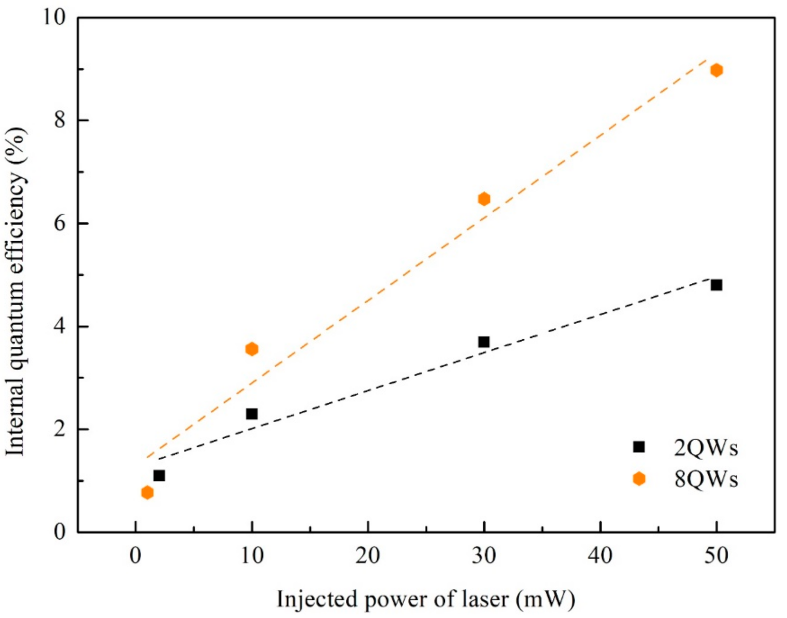
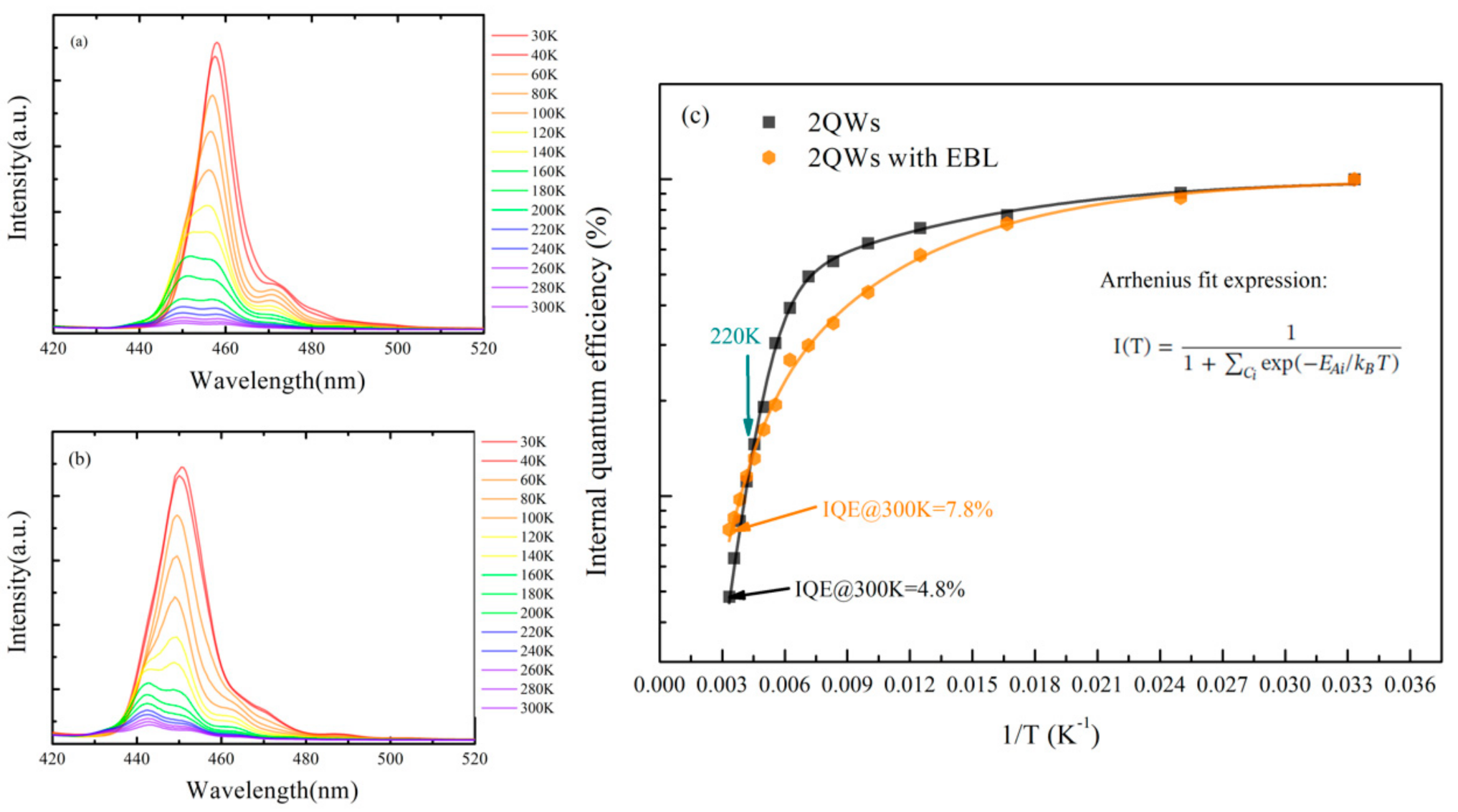
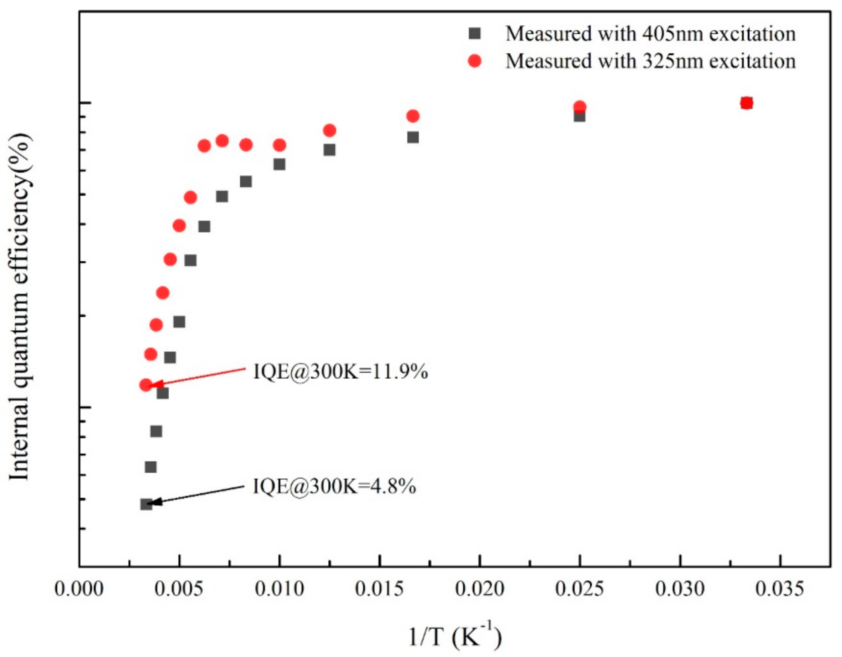
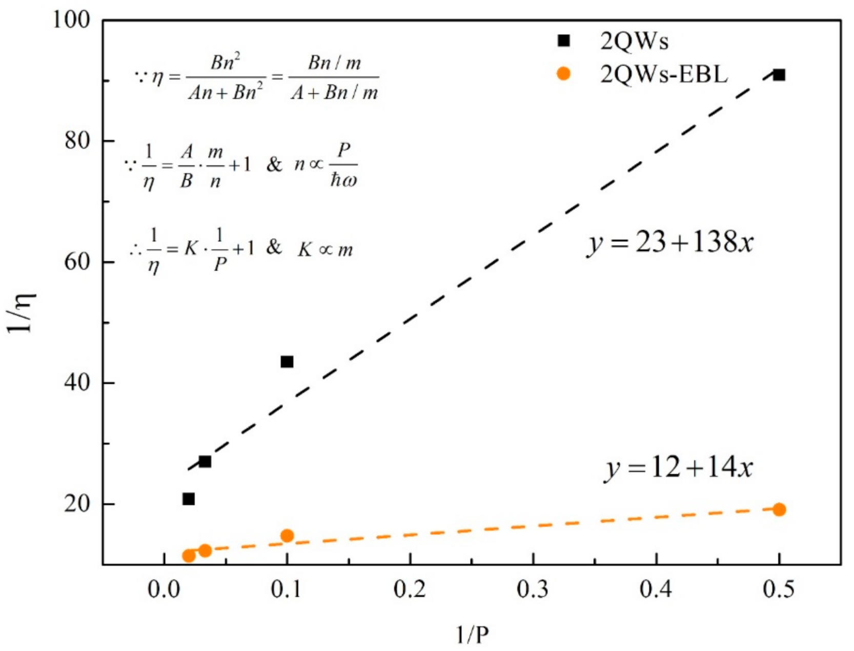
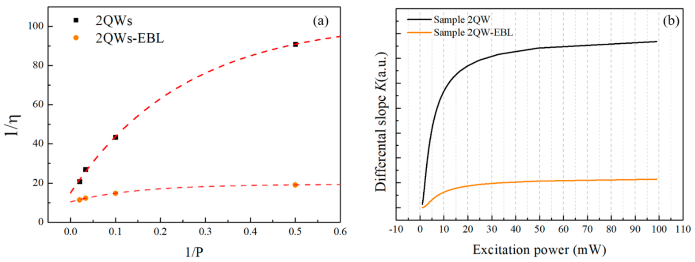
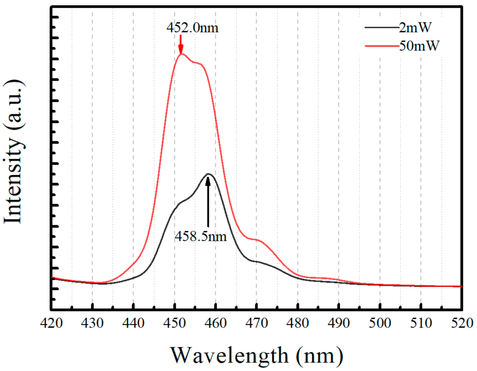
3.1. The Effect of Carrier Leakage on IQE

Figure 1 shows the internal quantum efficiency (IQE) at room-temperature under different excitation power for sample 2QW and 8QW, respectively. The IQE was measured under the 405 nm laser excitation. Significantly, the IQE increases with increasing excitation power, which is mainly caused by increased carrier concentration (the mechanism will be discussed below). It is worth noting that under quite low excitation power, such as around 1 mW, the IQE of sample 2QW and 8QW is close. However, under higher excitation power, e.g., 50 mW, the IQE of sample 8QW is much higher than that of 2QW and the IQE is 9.0% and 4.8%, respectively. For clearer understanding, a rough liner fitting, shown the trend of the increase of IQE with excitation power, is presented in Figure 1 as guides to eyes. Obviously, the fitting slope for sample 8QW is larger than that of sample 2QW. It is suggested that a higher increase rate of IQE with increasing excitation power appears in sample 8QW. The reason that led to the different excitation power dependence of IQE for the two samples will be discussed below in detail.
According to the ABC models, the internal quantum efficiency η is commonly expressed as below [9,12,21]:
η = B n A + B n + C n 2
where the constant A corresponding to the Shockley–Read–Hall (SRH) non-radiative recombination process, the constant B corresponding to the bimolecular radiative recombination process, and the constant C associated with the non-radiative Auger recombination are assumed to be nearly independent of the carrier concentration n. When the temperature is 0 K, the IQE is considered to be 100% due to the totally suppressed non-radiative recombination [22,23]. Since the integrated PL intensity I B n , a common method to measure the IQE is used in this work, which can be written as [19]:
η T = I T / I 0
When the MQWs is pumped by optical laser source, the non-radiative Auger recombination is generally ignored due to the small Auger coefficient C [9,24]. The Equation (1) can be written to:
η = B n A + B n
According to Equation (3), the IQE will increase with increasing carrier concentration n due to the enhanced radiative recombination, which is corresponded to the increase trend of IQE versus excitation power as shown in Figure 1. Meanwhile, Figure 1 shows the higher IQE for 8QW at higher excitation power. Two aspects may be related to the higher IQE of sample 8QW. On one hand, when the excitation power is the same, the carrier concentration in the quantum well is generally assumed to be the same due to the close light absorption coefficient in the same material. As a result, the IQE is mainly determined by the non-radiative recombination coefficient A, which corresponds to the non-radiative SRH recombination. Strong non-radiative SRH recombination is the main reason to the low IQE as reported in the literature [11,17].
To check that, Figure 2 presents the micro-PL comparison, in which the non-radiative recombination can be characterized by the non-luminescent area such as black spots. Unexpectedly, the non-radiative recombination got enhanced in sample 8QW as shown in Figure 2b, in which the black spots is so much that it presents an obvious labyrinth-like pattern comprised of bright and dark regions, while the black spots are less in Figure 2a for sample 2QW. The worse quality of sample 8QW may be caused by the longer high temperature growth process via MOCVD. The results indicates that the higher IQE in sample 8QW may be not related to weaken non-radiative SRH recombination. It is necessary to mention that the luminescence intensity of sample 8QW is stronger than that of sample 2QW due to the higher quantum well number. In order to observe the non-radiative area in micro-PL, the laser power and gain value is different for the measurement of the two samples. Therefore, the picture of Figure 2b is darker.
On the other hand, the increase of IQE may be caused by the increase of carrier concentration. One should note that to drive the ABC model, a crucial assumption is that the carrier leakage from active region is negligible [9]. However, if the carrier leakage is reconsidered, the above results can be well explained. Figure 3 shows the schematic diagram of conduction band and carrier leakage pathway in sample 2QW and 8QW. For sample 2QW, carriers are easily leak out of active regions, leading to decrease of carrier concentration n. However, for sample 8QW, carriers leaking out of quantum wells could be recaptured by adjacent quantum wells. The carrier leakage will be suppressed in sample 8QW and the carrier concentration n in sample 8QW will be higher than that of sample 2QW. The increased carrier concentration will enhance the radiative recombination process, resulting the increase of IQE. Meanwhile, the carrier leakage is widely accepted to be aggravated with increase of excitation power. In sample 8QW, the carrier leakage is suppressed, leading to a faster increase trend of IQE with the increasing excitation power.
Although introducing carrier leakage can well explain the unexpected increase of IQE of sample 8QW. However, it is not clear whether the increase of well layers will cause other influencing factors. Recently, researchers reported similar trend of IQE with increasing well numbers, which is attributed to the less non-radiative recombination centers caused by increase of total InGaN thickness [25]. Despite that the worse quality shown in Figure 2 disagrees with less non-radiative recombination centers, the carrier leakage mechanism in GaN-based MQW should get further verification, getting rid of the influence of total InGaN thickness. A new-designed sample with electron blocking layer (EBL), named as sample 2QW-EBL, was grown by MOCVD. The growth conditions of MQW of sample 2QW-EBL are totally identical to the sample 2QW, which is aimed to exclude most of the influencing factors in MQW between the two samples (such as the total InGaN thickness). After the grown of MQW, a very thin AlGaN EBL was deposited in sample 2QW-EBL. Figure 4 shows the contrast of conduction band and carrier transfer pathway in sample 2QW and 2QW-EBL. Since the higher bandgap energy of AlGaN, a potential energy barrier formed in AlGaN EBL can effectively block the leakage of electrons and increase the possibility of recapture of electrons. Therefore, if the inferences above are solid, the IQE of sample 2QW-EBL will be obvious higher than that of sample 2QW.
Figure 5a,b shows the TDPL spectra from 30 to 300 K for sample 2QW and 2QW-EBL, and Figure 5c presents IQE results derived from the TDPL spectra. The IQE at room temperature of sample with EBL is 7.8%, much higher than that of sample 2QW, which is 4.8%. The result consolidates the carrier leakage mechanism mentioned above. The results will be discussed in detail below.
Figure 6 shows the micro-PL comparison of sample 2QW and 2QW-EBL, a kind of huge black spots appears in Figure 6b as marked by red circle. Theoretically, the MQW of both samples should be almost the same due to the same growth conditions. However, in factual epitaxial growth via MOCVD, the effect caused by subsequent layers on the MQW is inevitable. In sample 2QW-EBL, a AlGaN EBL was deposited on the MQW to hinder the carrier leakage process. However, the higher growth temperature of AlGaN may Aggravate the phase segregation of indium in InGaN/GaN MQW. The above results suggest that the sample 2QW-EBL has a worse quality which should decrease the IQE. However, the sample 2QW-EBL has a higher IQE at room temperature. It is a more persuasive support to the carrier leakage mechanism.
Another interesting result is that the IQE measured using 325 nm laser source is much higher than that using 405 nm laser source, as shown in Figure 7. The excitation power of 325 nm laser is 3 mW, which is much lower than that of 405 nm laser which is 50 mW. However, the IQE measured under 325 nm laser is 11.9%, while it is 4.8% when measured under 405 nm laser. As well known, the carriers in quantum barrier layers can be excited by 325 nm laser, which may be injected into quantum wells, thus, the carrier concentration increases significantly. As a result, the IQE when using 325 nm laser source is higher than that with 405 nm laser. The physical mechanism has been discussed in detail in our previous work [26]. Here, the injected carrier can also significantly enhance the IQE, which provide evidence to the huge effect of carrier leakage on the IQE from an opposite direction.

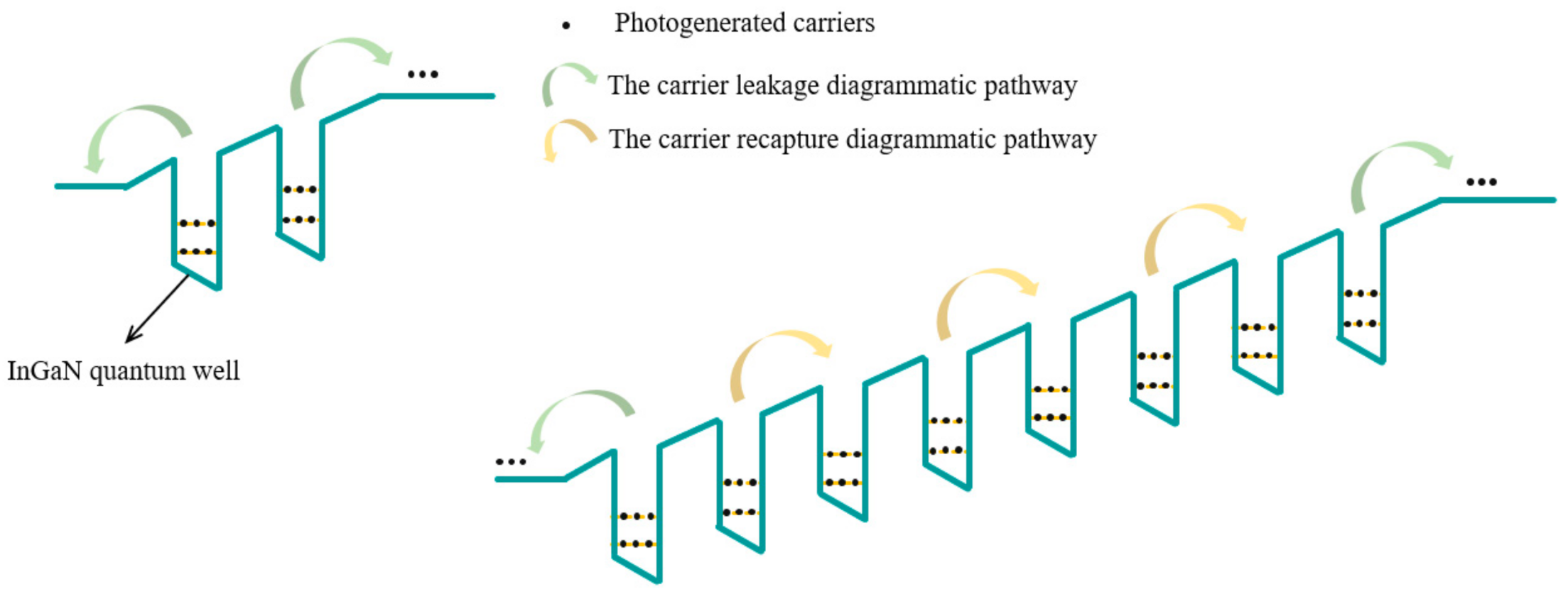
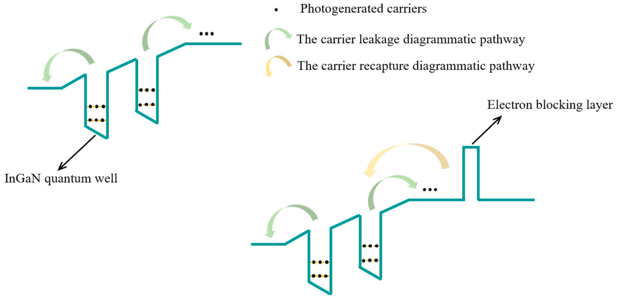
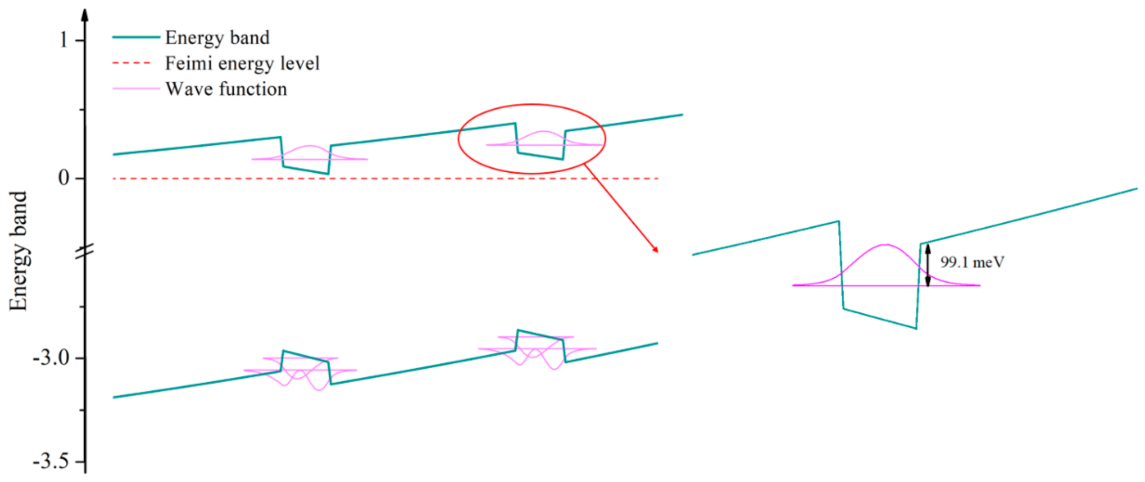
3.2. The Physical Mechanism of Carrier Leakage in GaN-Based MQW

In Figure 5c, we also found that the IQE decays with increase of temperature for both sample, which is caused by the activation of non-radiative centers [22]. However, the decay rate of IQE is much different between the sample 2QW and 2QW-EBL. In the early stages of temperature rising, the decay rate of IQE for sample 2QW-EBL is faster than sample 2QW. However, when temperature rises further, the decay rate for sample 2QW increase rapidly and the IQE of sample 2QW is lower than sample 2QW-EBL when temperature is beyond 220K. The decay process is corresponding to the Arrhenius equation which is written as [27,28]:
I T = 1 1 + c i exp E A i / k B T
where the EAi corresponds to the activation energy of non-radiative recombination centers, and the Ci is the constant related to the density of these centers.
The fitting results are presented in Table 1 and two noteworthy points will be discussed below. Firstly, there is a new kind of non-radiative centers whose activation energy is 34.8 meV in sample 2QW-EBL compared to sample 2QW. As mentioned above, sample 2QW-EBL has a worse quality of MQW and a kind of huge black spots appears in Figure 6b as marked by red circle. The huge black spots may be related to more serious phase segregation of indium in MQW caused by high growth temperature of AlGaN EBL. Relatively, the new kind of non-radiative centers in sample 2QW-EBL may origin from the worse quality of MQW.
Secondly, the IQE of sample 2QW decays faster than that of sample 2QW-EBL when temperature is beyond 220 K. Considering the structure design to hinder the carrier leakage in sample 2QW-EBL, it is safe to say the carrier leakage mechanism dominating the higher temperature stage and the activation energy is around 100 meV. When temperature is low, such as 30 K, the carriers are frozen. The possibility of carriers leaked out of quantum well is negligible. The dominant non-radiative recombination centers are mainly corresponding to the defects and dislocations in MQW. Due to the worse quality as shown in Figure 6b, the decay of IQE of sample 2QW-EBL is faster than that of sample 2QW at lower temperature stage. As temperature rises, the possibility of carrier leakage will increase. As a result, the IQE of sample 2QW decreases dramatically at higher temperature stage. However, for sample 2QW-EBL, the carriers are blocked by the AlGaN EBL, leading to an obvious improvement of IQE at higher temperature stage due to increase carrier concentration.
To further investigate the dependence of carrier leakage on excitation power, a leakage factor m is introduced into the Equation (3) and the new equation can be expressed as:
η = B n / m A + B n / m
When leakage factor m is 1, the carrier leakage process does not exist in a MQW sample, corresponding to the assumption of no carrier leakage in ABC-model. All the injection carriers participate in the radiative recombination process or non-radiative recombination process. When the m is greater than 1, meaning that a certain proportion of carriers leaked out of well layers. As the decrease of carriers will mainly weaken the radiative recombination process, the IQE will decrease with the increase of leakage factor m. The Equation (5) can be further deformed to:
1 η = A · m B · 1 n + 1
Assuming the conversion efficiency of photons into electrons is constant, since the photon density is proportional to excitation power P, the Equation (6) can be roughly written as:
1 η = K · 1 P + 1 & K A · m B  
Through Equation (7), the leakage factor can be analyzed qualitatively by the slope K. Figure 8 shows the data and linear fitting of reciprocal of IQE versus the reciprocal of excitation power for sample 2QW and 2QW-EBL. The slope K of sample 2QW-EBL is around one-tenth of sample 2QW. Assuming the similar ratio of non-radiative SRH recombination coefficient and radiative recombination coefficient A/B of MQW for the two samples, the degree of carrier leakage in sample 2QW-EBL is much lower than that of sample 2QW (considering the worse quality of MQW for sample 2QW-EBL, the carrier leakage in sample 2QW-EBL will be less.) However, the intercept is obviously higher than 1 and the linearity of the data is unsatisfactory. The slope K decreases with decreasing excitation power as pointed by the data shown in Figure 8. The results may indicate that the leakage factor m is dependent to the excitation power.
Figure 9a further presents the non-linear fitting results based on the least square method and the differential slope K is calculated and shown in Figure 9b, which obviously increases with increasing excitation power. The result indicates that the carriers leaked out of MQW may increase with increasing excitation power. Figure 10 shows the PL spectra of sample 2QW with 2 and 50 mW excitation laser power under 160 K. Significantly, the peak wavelength with 50 mW excitation laser power decrease from 458.5 nm to 452 nm, indicating a higher peak energy of PL spectra. When excitation power increases, electrons have a higher possibility to occupy localized states with higher energy [29], thus the recombination energy is higher with 50 mW excitation laser power. As a result, the quantum barrier height restricting carriers reduces and the electrons are easier to leak out of quantum wells. Meanwhile, we can find that differential slope K increases rapidly at low power stage, then slow down at higher power stage, suggesting that the carrier leakage is turn on at low excitation power and reach the saturation at higher excitation power. Such a turn-on excitation power is below 10 mW, indicating that the carriers leaked out of MQW is much easier than expectation in InGaN/GaN MQW under the optical excitation.
To understand why the carrier leakage happens easily in InGaN/GaN MQW, a simulation calculation of energy band structure of InGaN/GaN MQW are conducted by LASTIP program (Crosslight Software Inc., Burnaby, BC, Canada). The MQW parameters are corresponding to the HRXRD measurement results of sample 2QW (which has been listed above): the indium composition and thickness of well layers is determined to be 10.0% and 3 nm, while it is 2% and 11 nm in barrier layers, respectively. Figure 11 presents the calculated energy band structure, and we can find that only ground state energy level exists in In0.1Ga0.9N quantum well and the potential energy barrier hindering the carrier leakage is only 100 meV, which is in good agreement to the activation energy (91–102 meV) via Arrhenius fitting of temperature dependence of IQE. The higher energy gap between the ground state energy level and conduction band minimum is mainly caused by the small effective electron mass (m*) of InGaN and the narrow thickness of quantum well. According to the reports in the literature, the m* of GaN is 0.22 m0, while it is 0.11 m0 [30,31] (the m0 represents the free electronic mass) for the InN. Additionally, in this work, the quantum well thickness is as low as 3 nm. According to a simplified model of infinite deep square potential well, the discrete energy levels above the conduction band edge are in inverse proportion to the effective electron mass and square of quantum well thickness. The small effective electron mass of InGaN and the narrow thickness leads to a more prone carrier leakage mechanism in InGaN/GaN quantum well.

4. Conclusions

In summary, the IQE measurement derived from the ABC-model has its limitations in characterizing the SRH non-radiative recombination process in MQW. MQW samples with enhanced non-radiative SRH recombination could have higher IQE via structure design optimization (such as EBL and increase of well layers). The key factor is the carrier leakage mechanism which was normally neglected under optical excitation. By blocking the carrier leakage, the sample with EBL has a much higher IQE even through the non-radiative SRH recombination is stronger in this sample. Moreover, the carrier leakage process will be turned on below the 220 K or 10 mW. Such a low turn-on temperature and power in InGaN/GaN MQW is mainly caused by the small effective electron mass of InGaN (0.11–0.22 m*) and the narrow thickness of quantum well.

Author Contributions

Conceptualization, Y.B. and D.Z.; methodology, Z.L.; software, Y.B.; validation, D.Z. and F.L.; formal analysis, Y.B.; investigation, Y.B.; resources, D.Z.; data curation, F.L.; writing—original draft preparation, Y.B.; writing—review and editing, F.L., J.Y. and P.C.; visualization, F.L.; supervision, F.L.; project administration, D.Z.; funding acquisition, D.Z. All authors have read and agreed to the published version of the manuscript.

Funding

This work was supported by the National Key R&D Program of China (Grant No. 2021YFF0307403), the National Natural Science Foundation of China (Grant Nos. 62034008, 62074142, 62074140, 61974162, 61904172, 61874175, 62127807), Beijing Nova Program (Grant No. 202093), the Strategic Priority Research Program of Chinese Academy of Sciences (Grant No. XDB43030101), Beijing Municipal Science& Technology Commission, Zhongguancun Science Park (Z211100004821001), and the Youth Innovation Promotion Association of Chinese Academy of Sciences (Grant No. 2019115).

Institutional Review Board Statement

Not applicable.

Informed Consent Statement

Not applicable.

Data Availability Statement

The data that support the findings of this study are available from the corresponding author upon reasonable request.

Conflicts of Interest

The authors declare no conflict of interest.

References

  1. Nakamura, S.; Senoh, M.; Nagahama, S.; Iwasa, N.; Yamada, T.; Matsushita, T.; Kiyoku, H.; Sugimoto, Y. InGaN-based multi-quantum-well-structure laser diodes. Jpn J. Appl. Phys. 1996, 35, L74–L76. [Google Scholar] [CrossRef]
  2. Kim, K.S.; Son, J.K.; Lee, S.N.; Sung, Y.J.; Paek, H.S.; Kim, H.K.; Kim, M.Y.; Ha, K.H.; Ryu, H.Y.; Nam, O.H.; et al. Characteristics of long wavelength InGaN quantum well laser diodes. Appl. Phys. Lett. 2008, 92, 101103. [Google Scholar] [CrossRef]
  3. Nakatsu, Y.; Nagao, Y.; Kozuru, K.; Hirao, T.; Okahisa, E.; Masui, S.; Yanamoto, T.; Nagahama, S.-I. High-efficiency blue and green laser diodes for laser displays. In Proceedings of the Gallium Nitride Materials and Devices XIV, San Francisco, CA, USA, 2–7 February 2019; International Society for Optics and Photonics: Bellingham, WA, USA, 2019; Volume 10918, p. 109181. [Google Scholar]
  4. Masui, S.; Nakatsu, Y.; Kasahara, D.; Nagahama, S.I. Recent improvement in nitride lasers. In Proceedings of the Gallium Nitride Materials and Devices XII, San Francisco, CA, USA, 28 January–2 February 2017; International Society for Optics and Photonics: Bellingham, WA, USA, 2017; Volume 10104, p. 101041. [Google Scholar]
  5. Feng, L.; Degang, Z.; Zongshun, L.; Ping, C.; Jing, Y.; Lihong, D.; Yongsheng, S.; Hai, W. GaN-based blue laser diode with 6.0 W of output power under continuous-wave operation at room temperature. J. Semicond. 2021, 42, 112801. [Google Scholar]
  6. Wu, J. When group-III nitrides go infrared: New properties and perspectives. J. Appl. Phys. 2009, 106, 5. [Google Scholar] [CrossRef]
  7. Lee, C.M.; Zhang, C.; Cantore, M.; Farrell, R.M.; Oh, S.H.; Margalith, T.; Speck, J.S.; Nakamura, S.; Bowers, J.E.; DenBaars, S.P. 4 Gbps direct modulation of 450 nm GaN laser for high-speed visible light communication. Opt. Express 2015, 23, 16232–16237. [Google Scholar] [CrossRef]
  8. Goldberg, G.R.; Ivanov, P.; Ozaki, N.; Childs, D.T.D.; Hogg, R.A. Gallium nitride light sources for optical coherence tomography. In Proceedings of the Gallium Nitride Materials and Devices XII, San Francisco, CA, USA, 28 January–2 February 2017; International Society for Optics and Photonics: Bellingham, WA, USA, 2017; Volume 10104, p. 101041. [Google Scholar]
  9. Karpov, S. ABC-model for interpretation of internal quantum efficiency and its droop in III-nitride LEDs: A review. Opt. Quant. Electron. 2015, 47, 1293–1303. [Google Scholar] [CrossRef]
  10. Dai, Q.; Schubert, M.F.; Kim, M.H.; Kim, J.K.; Schubert, E.F.; Koleske, D.D.; Crawford, M.H.; Lee, S.R.; Fischer, A.J.; Thaler, G.; et al. Internal quantum efficiency and nonradiative recombination coefficient of GaInN/GaN multiple quantum wells with different dislocation densities. Appl. Phys. Lett. 2009, 94, 111109. [Google Scholar] [CrossRef] [Green Version]
  11. Langer, T.; Chernikov, A.; Kalincev, D.; Gerhard, M.; Bremers, H.; Rossow, U.; Koch, M.; Hangleiter, A. Room temperature excitonic recombination in GaInN/GaN quantum wells. Appl. Phys. Lett. 2013, 103, 202106. [Google Scholar] [CrossRef]
  12. Podlipskas, Z.; Aleksiejunas, R.; Kadys, A.; Mickevicius, J.; Jurkevicius, J.; Tamulaitis, G.; Shur, M.; Shatalov, M.; Yang, J.; Gaska, R. Dependence of radiative and nonradiative recombination on carrier density and Al content in thick AlGaN epilayers. J. Phys. D Appl. Phys. 2016, 49, 145110. [Google Scholar] [CrossRef]
  13. Narukawa, Y.; Kawakami, Y.; Funato, M.; Fujita, S.; Fujita, S.; Nakamura, S. Role of self-formed InGaN quantum dots for exciton localization in the purple laser diode emitting at 420 nm. Appl. Phys. Lett. 1997, 70, 981–983. [Google Scholar] [CrossRef]
  14. Nakamura, S. The roles of structural imperfections in InGaN-Based blue light-emitting diodes and laser diodes. Science 1998, 281, 956–961. [Google Scholar] [CrossRef] [PubMed] [Green Version]
  15. Hangleiter, A.; Hitzel, F.; Netzel, C.; Fuhrmann, D.; Rossow, U.; Ade, G.; Hinze, P. Suppression of nonradiative recombination by V-shaped pits in GaInN/GaN quantum wells produces a large increase in the light emission efficiency. Phys. Rev. Lett. 2005, 95, 127402. [Google Scholar] [CrossRef] [PubMed] [Green Version]
  16. Der Maur, M.A.; Pecchia, A.; Penazzi, G.; Rodrigues, W.; di Carlo, A. Efficiency Drop in Green InGaN/GaN Light Emitting Diodes: The Role of Random Alloy Fluctuations. Phys. Rev. Lett. 2016, 116, 027401. [Google Scholar] [CrossRef] [PubMed] [Green Version]
  17. Peng, L.; Zhao, D.; Zhu, J.; Wang, W.; Liang, F.; Jiang, D.; Liu, Z.; Chen, P.; Yang, J.; Liu, S.; et al. Achieving homogeneity of InGaN/GaN quantum well by well/barrier interface treatment. Appl. Surf. Sci. 2020, 505, 144283. [Google Scholar] [CrossRef]
  18. Laak, N.K.V.D.; Oliver, R.A.; Kappers, M.J.; Humphreys, C.J. Role of gross well-width fluctuations in bright, green-emitting single InGaN/GaN quantum well structures. Appl. Phys. Lett. 2007, 12, 121911. [Google Scholar] [CrossRef]
  19. Oto, T.; Banal, R.G.; Kataoka, K.; Funato, M.; Kawakami, Y. 100 mW deep-ultraviolet emission from aluminium-nitride-based quantum wells pumped by an electron beam. Nat. Photonics 2010, 4, 767–771. [Google Scholar] [CrossRef]
  20. Wang, X.; Liang, F.; Zhao, D.; Jiang, D.; Liu, Z.; Zhu, J.; Yang, J.; Wang, W. Effect of dual-temperature-grown InGaN/GaN multiple quantum wells on luminescence characteristics. J. Alloys Compd. 2019, 790, 197–202. [Google Scholar] [CrossRef]
  21. Piprek, J. Efficiency droop in nitride-based light-emitting diodes. Phys. Status Solidi A 2010, 207, 2217–2225. [Google Scholar] [CrossRef]
  22. Huang, K.; Rhys, A. Theory of Light Absorption and Non-Radiative Transitions in F-Centres. Proc. R. Soc. Lon. Ser. A 1950, 204, 406–423. [Google Scholar]
  23. Miller, R.C.; Kleinman, D.A.; Nordland, W.A., Jr.; Gossard, A.C. Luminescence Studies of Optically Pumped Quantum Wells in GaAs-AlxGal-x As Multilayer Structures. Phys. Rev. B 1980, 22, 863–871. [Google Scholar] [CrossRef]
  24. Vaxenburg, R.; Lifshitz, E.; Efros, A. Suppression of Auger-stimulated efficiency droop in nitride-based light emitting diodes. Appl. Phys. Lett. 2013, 102, 031120. [Google Scholar] [CrossRef]
  25. Zhou, R.L.; Ikeda, M.; Zhang, F.; Liu, J.P.; Zhang, S.M.; Tian, A.Q.; Wen, P.Y.; Li, D.Y.; Zhang, L.Q.; Yang, H. Total-InGaN-thickness dependent Shockley-Read-Hall recombination lifetime in InGaN quantum wells. J. Appl. Phys. 2020, 127, 013103. [Google Scholar] [CrossRef]
  26. Ben, Y.; Liang, F.; Zhao, D.; Wang, X.; Yang, J.; Liu, Z.; Chen, P. Anomalous Temperature Dependence of Photoluminescence Caused by Non-Equilibrium Distributed Carriers in InGaN/(In)GaN Multiple Quantum Wells. Nanomaterials 2021, 11, 1023. [Google Scholar] [CrossRef] [PubMed]
  27. Leroux, M.; Grandjean, N.; Beaumont, B.; Nataf, G.; Semond, F.; Massies, J.; Gibart, P. Temperature quenching of photoluminescence intensities in undoped and doped GaN. J. Appl. Phys. 1999, 86, 3721–3728. [Google Scholar] [CrossRef]
  28. Yasan, A.; McClintock, R.; Mayes, K.; Kim, D.H.; Kung, P.; Razeghi, M. Photoluminescence study of AlGaN-based 280 nm ultraviolet light-emitting diodes. Appl. Phys. Lett. 2003, 83, 4083–4085. [Google Scholar] [CrossRef]
  29. Xing, Y.; Zhao, D.; Jiang, D.; Liu, Z.; Zhu, J.; Chen, P.; Yang, J.; Liang, F.; Liu, S.; Zhang, L. Carrier Redistribution Between Two Kinds of Localized States in the InGaN/GaN Quantum Wells Studied by Photoluminescence. Nanoscale Res. Lett. 2019, 14, 88. [Google Scholar] [CrossRef]
  30. Witowski, A.M.; Pakuła, K.; Baranowski, J.M.; Sadowski, M.L.; Wyder, P. Electron effective mass in hexagonal GaN. Appl. Phys. Lett. 1999, 75, 4154–4155. [Google Scholar] [CrossRef]
  31. Morkoç, H. Nitride Semiconductor Devices: Fundamentals and Applications; Wiley: Hoboken, NJ, USA, 2013. [Google Scholar]
Figure 1. The internal quantum efficiency of sample 2QW and 8QW under different excitation power; the dotted lines are guides to eyes.
Crystals 12 00171 g001
Figure 2. The micro-PL images of GaN-based MQW samples with two quantum wells (a) and eight quantum wells (b).
Crystals 12 00171 g002
Figure 3. The schematic diagram of conduction band and carrier leakage pathway in sample 2QW and 8QW. Due to the larger number of well layers of sample 8QW, the carriers leaking out of quantum well are more likely to be recapture by another quantum well.
Crystals 12 00171 g003
Figure 4. The schematic diagram of conduction band and carrier leakage pathway in sample 2QW and 2QW-EBL.
Crystals 12 00171 g004
Figure 5. The TDPL spectra from 30 to 300 K for sample 2QW (a) and 2QWEBL (b); the trend of internal quantum efficiency with increasing temperature from 30 to 300 K (c); the lines are corresponding to the Arrhenius fitting. The IQE is derived by calculated the ratio of integrated luminescence intensity at room temperature and that at low temperature (here is 30 K).
Crystals 12 00171 g005
Figure 6. The micro-PL images of GaN-based MQW samples 2QW (a) and 2QW-EBL (b); the huge black spots shown in the red circle may correspond to the new kind of non-radiative recombination centers.
Crystals 12 00171 g006
Figure 7. The trend of internal quantum efficiency of sample 2QW under different wavelength excitation sources.
Crystals 12 00171 g007
Figure 8. The data and fitting line of reciprocal of IQE versus the reciprocal of excitation power for sample 2QW and 2QW-EBL.
Crystals 12 00171 g008
Figure 9. The non-linear fitting results based on the least square method (a) and the differential slope K versus excitation laser power (b).
Crystals 12 00171 g009
Figure 10. The PL spectra of sample 2QW with 2 and 50 mW excitation laser power under low temperature.
Crystals 12 00171 g010
Figure 11. The calculated energy band structure via simulation software LASTIP.
Crystals 12 00171 g011
Table 1. The fitting results.
SampleC1EA1/meVC2EA2/meVC3EA3/meV
2QW2.0210.51026102.7//
2QW-EBL4.1912.523091.413.5534.8
Publisher’s Note: MDPI stays neutral with regard to jurisdictional claims in published maps and institutional affiliations.

