1. Introduction
GaN-based nitrides have achieved great success in solid state lighting because of their wide and direct band gap properties [
1]. So far, various optoelectronic devices based on GaN-based materials have been developed. For examples, GaN-based light sources from green to ultraviolet have been realized, and they have broad application potential in the fields of lighting, display, biomedicine, high-density data storage, and laser application [
2,
3,
4].
It has been well-known that the light emission in a semiconductor can be from either spontaneous recombination or simulated recombination, and the excitons always play the key role. In addition to the normal spontaneous recombination or simulated recombination, the excitons can also couple with photons to form a new hybrid structure, which is proposed theoretically by Hopfield in 1950s [
5]. According to the strength of the coupling, it can be divided into strong coupling and weak coupling. When the excitons and photons are designated weak coupling, it mainly affects the radiation recombination rate of the original spontaneous recombination. In weak coupling, the probability of photons being bonded by excitons is extremely low, and the entire system is a dissipative system. In contrast, in strong coupling, the probability of photons being bund by excitons is very high. Then, the exciton-photon complex will appear and no longer follow the rule of original spontaneous recombination. To achieve strong coupling, the probability of photons coupling with excitons must be greater than the probability of photons escaping from the cavity. For the solution, one is to use long-lifetime excitons, which is an easy condition for InGaN material (with a large binding energy and relative longer exciton lifetime). The other one is to increase the staying time of photons, which means the strong confinement of the photons. Obviously, with a good optical cavity, photons can be effectively confined. Then, finally, when a InGaN-based quantum wells (QW) is placed in a good optical cavity [
6], the coupling between excitons and photons can be increased. If the coupling strength increases further, an exciton polariton can be formed, and even reach the state of Bose–Einstein condensate (BEC) under certain conditions. These properties have a wide range of applications, such as ultra-low threshold polariton lasers [
7,
8,
9].
Group III nitride semiconductors have a large amount of exciton binding energy (26 meV for bulk GaN and 40 meV for narrow quantum well QW). Some studies have indicated that GaN can achieve exciton-polariton at room-temperature in a microcavity with double distributed Bragg reflectors (DBR) [
10,
11,
12]. S. Christopoulos et al. studied the exciton-polariton emission in a GaN microcavity. The result of a low-threshold coherent emission was one order of magnitude smaller than that of the previously reported nitride-based VCSEL [
13]. In order to make the exciton–photon couple stronger, the restriction on photons must be strong enough, so it is necessary to explore new high-quality optical microcavity and easy to be realized. In the past research, different ridge-shape microcavities have been widely used to limit the distribution of photons in strip lasers [
14,
15]. For example, the common rectangular ridge microcavity can confine the light directly below the ridge. Zhong-Kai Zhang et al. found that a narrower ridge will provide stronger optical confinement for the lateral mode in the ridge and improve the far-field characteristics of the device [
16]. So, the ridge microcavity can be one of good candidatures, once achieving a strong photon confinement in a desired ridge shape. Compared with the usual rectangular ridge cavity, the triangular ridge cavity has a triangular cross section, which can furtherly concentrate the photons on the top part of the ridge. Clearly, this is beneficial to obtain high-efficiency photon localization in small volume.
In this paper, the triangular-like ridge cavity with InGaN/GaN MQWs inside is fabricated. It is found that the triangular-like ridge cavity with an appropriate apex angle can effectively confine photons, and abnormal emission signals confirm that a new transition channel appeared in the triangular-like ridge cavity.
2. Materials and Methods
The wafer used in our experiment is a standard blue LED wafer grown on a (0001) sapphire substrate by using the metal-organic chemical vapor deposition (MOCVD). From the substrate, a 25 nm GaN buffer layer was first grown. Above the buffer, a 4.5-μm n-type GaN layer was grown and followed by an 8-period InGaN/GaN (3 nm/12 nm) multiple quantum wells (MQWs) with the In composition of 15%. Finally, 320 nm p-type GaN was grown.
The fabrication process of the triangular-like ridge cavity is as follows: first, depositing 600 nm SiO2 on the wafer surface by plasma enhanced chemical vapor deposition (PECVD, Oxford, UK), and then transferring the device pattern to the SiO2 by photolithography and inductively coupled plasma (ICP, Oxford, UK) etching. Finally, uncovered GaN material was etched by ICP to form the ridge. In order to form a triangular cross-section, we mainly used Cl2/BCl3 to etch GaN while increasing the power of the ICP, and finally obtained a triangular-like ridge cavity with a larger sidewall inclination.
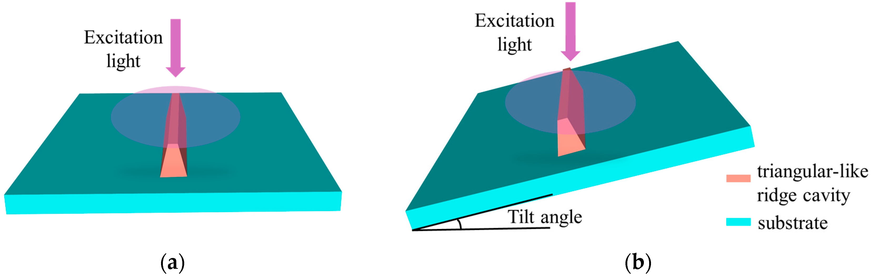
The optical properties of the triangular-like ridge cavity are measured by photoluminescence (PL), time-resolved photoluminescence (TR-PL), and angle-resolved photoluminescence (AR-PL). In the PL experiment, the excitation source is Mira900F femtosecond laser (Coherent Inc., Santa Clara, CA, USA). The laser wavelength is set at 375 nm, the pulse width is 140 fs, and the frequency is 76 MHz. The AR-PL is measured by an angle-resolved far-field emission spectroscopy microscope system (Shanghai, China). The excitation light source is a 405 nm semiconductor laser. The diameter of the light spot is adjusted by a microscope objective (Olympus 100x, NJ, USA) to cover the triangular ridges. The light emission of the triangular-like ridge cavity is also collected through the same objective lens. The measurement angle is limited by the numerical aperture (NA = 0.9) of the microscope objective to a range of ±60°. A fiber optic spectrometer (NOVA-EX, Shanghai, China) scans along the Fourier plane to collect angle-resolved far-field emission spectra. All measurements are performed at room-temperature.
3. Results
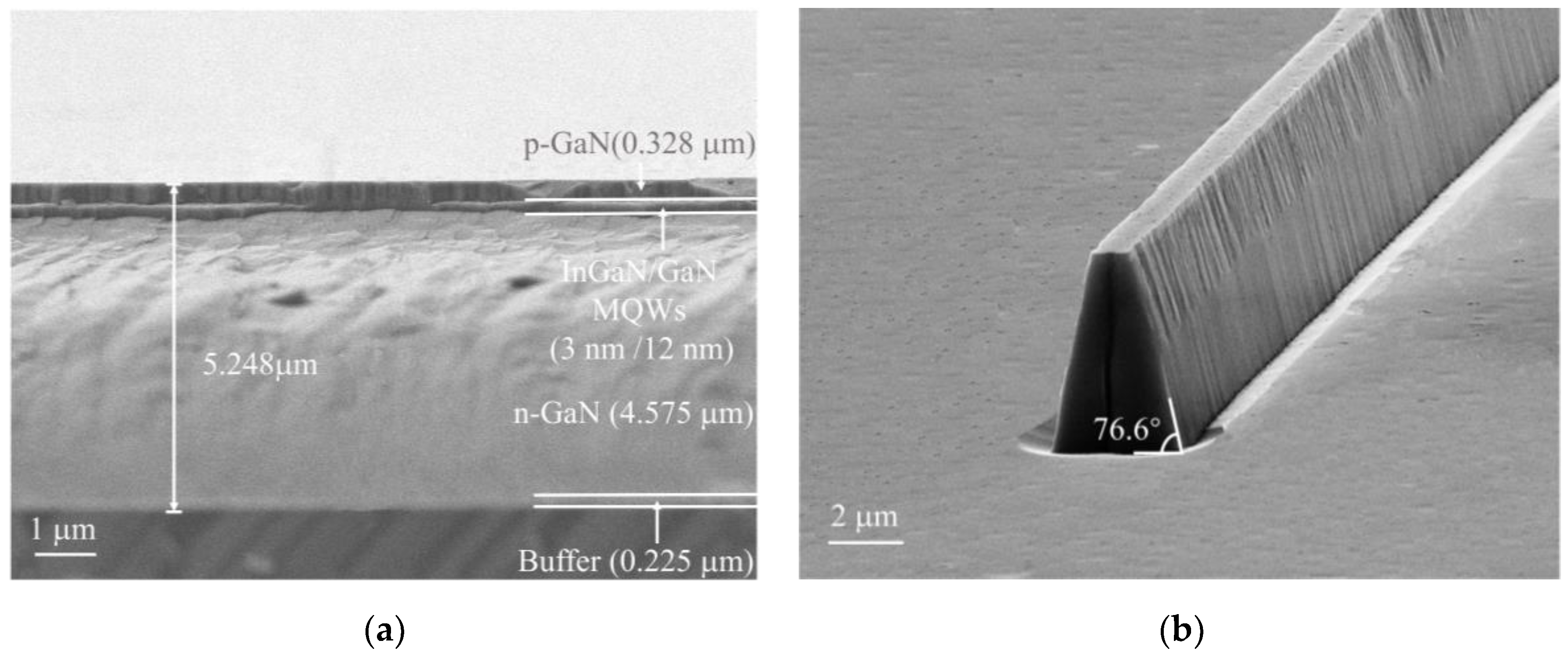
The morphology of the triangular-like ridge cavity was observed by scanning electron microscopy (SEM), as shown in
Figure 1. Since the distance between the MQWs and the wafer top surface is only 320 nm, the triangular ridge with a sharp top corner is not safe to the MQWs, which has a high possibility to be destroyed by the ion bombing through the inclined sidewall during the ICP etching. In order to ensure that the MQWs are not damaged by ICP etching, we have fabricated a triangular-like ridge cavity with small top flat surface about 0.9 μm wide, and the bottom side is 3.6 μm wide. The length of the ridge is 1000 μm. To further reduce the damage caused by ICP etching, we also adopted the low-damage etching parameters reported in our previous work [
17]. For reference, part of the wafer was protected during all process to keep original flat surface.
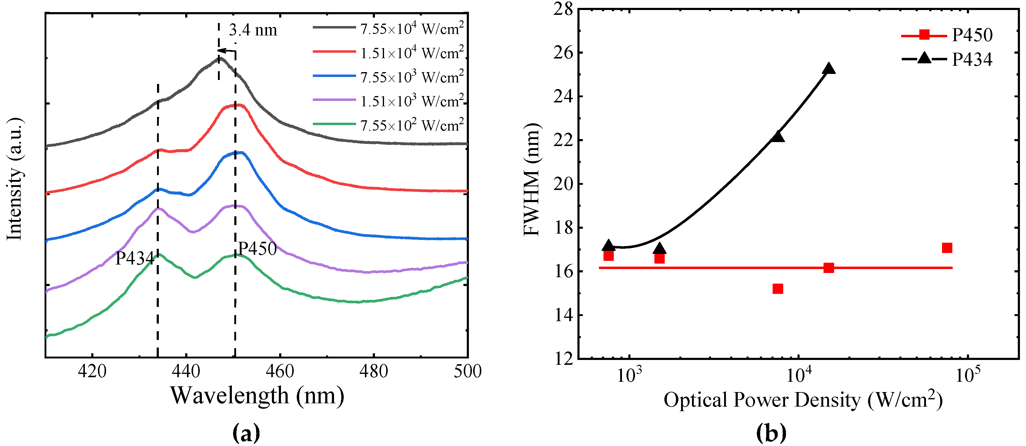
The PL spectrum of the triangular-like ridge cavity at room-temperature is shown in
Figure 2. In
Figure 2a, there are two emission peaks, located at 434 nm (P434) and 450 nm (P450), respectively. In the low-power excitation, the intensity of P434 is relatively stronger. As the excitation power increases, the intensity of P450 becomes higher. Meanwhile, the peak position of P434 does not move with the increase in excitation power, but P450 show a blue shift of 3.4 nm. It is well-known that there are many reasons for the blue-shift of the luminescence peak with increasing excitation, including the band-filling effect of quantum wells [
18,
19], and the quantum Stark effect [
20,
21]. Regardless, these results reflect that P434 and P450 may be different transitions. The original of the two peaks need to be judged in conjunction with other results, such as the full width at half maximum (FWHM) in the following study.
We obtained the FWHM of the P450 and P434 by Lorenzian fitting, as shown in
Figure 2b. It can be seen that the P434 FWHM keeps widening with the increase in excitation power, while the P450 FWHM is almost unchanged. According to previous studies, for a normal recombination process, the density of photo-generated carriers in MQWs becomes higher with the increase in the excitation power, and then involving more energy levels into the radiation transition, which leads to the broadening of the FWHM. Therefore, the increase in P434 FWHM with the increase in excitation power indicates that P434 is the usual spontaneous emission from the InGaN/GaN quantum wells. However, the P450 FWHM remains unchanged during all measurements, this indicates an unusual transition. The carriers in the microcavity should be affected by other factors, which change the original radiation mechanism.
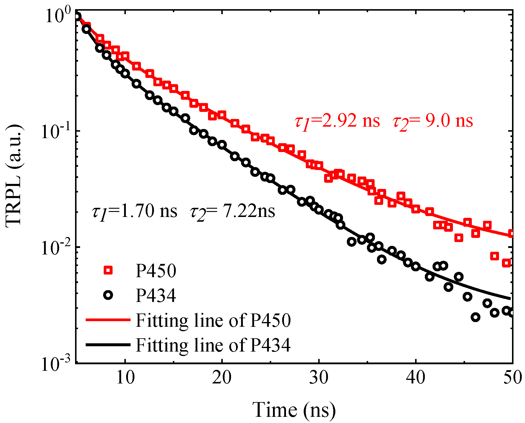
In order to further investigate the difference between P434 and P450, we measured the lifetime of P434 and P450 under different excitation powers at room temperature, one typical result was showed in
Figure 3. The data were fitted with a standard two-exponential component model described by Equation (1):
where
τ1 is fast decay components, and
τ2 is slow decay components [
22].
As shown in
Figure 3, the black and red solid lines are the fitting curves, and the lifetime of P450 is longer than that of P434, whatever for
τ1 or
τ2. At the excitation power of P = 1.25 kW/cm
2, we calculated that the
τ1 of P450 is 70% higher than that of P434, further confirming the different recombination mechanisms between P434 and P450. As discussed in
Figure 2, the behavior of FWHM has indicated that P434 is the usual spontaneous emission from the InGaN/GaN quantum wells. The only special figure of our sample is the ridge structure. As the simulation presented later, the top part of the ridge can accumulate high density of the light. Thus, we can see that the different background light density may contribute to the formation of P450, a new transition channel. This can explain the faster growth of P450 with the increase in excitation power, i.e., the number of photons in the ridge top part is increasing.
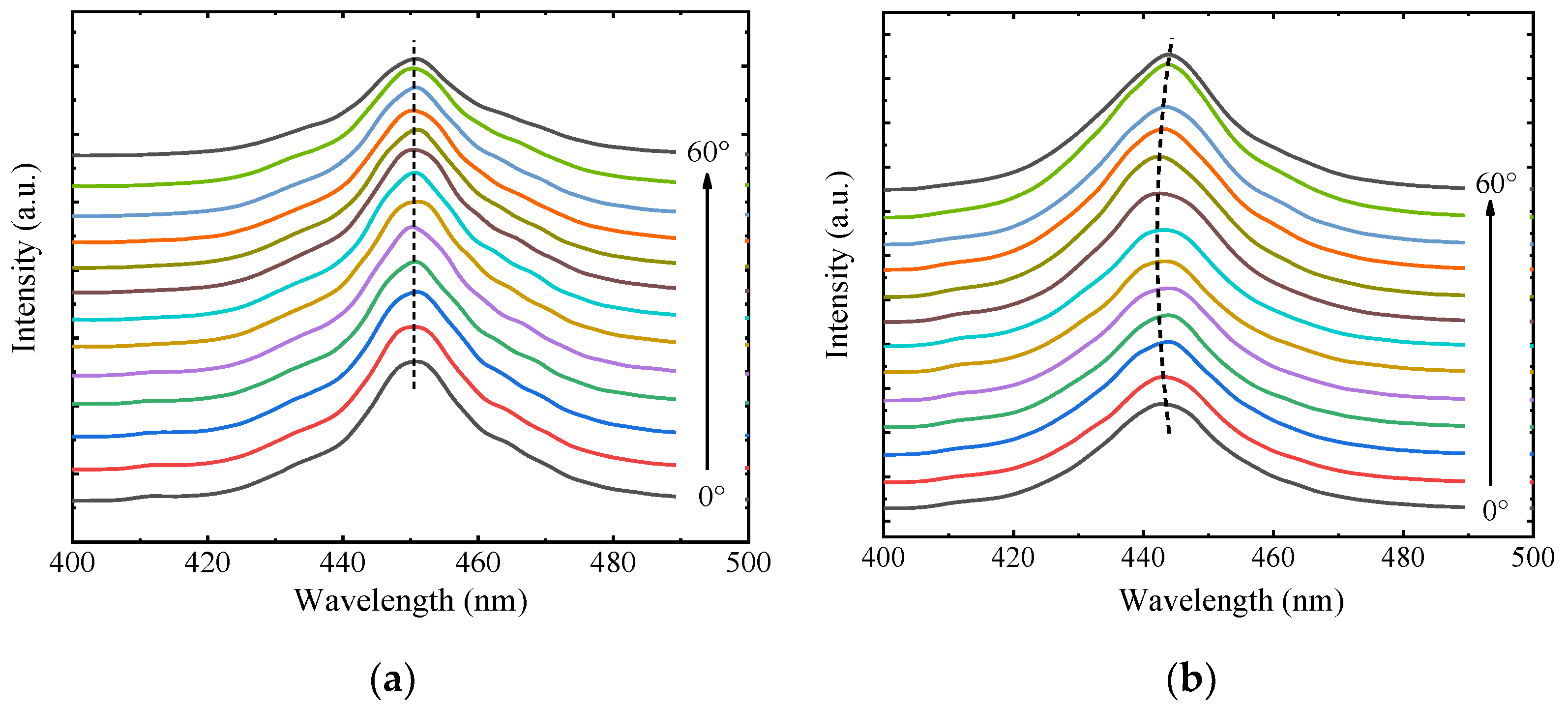
If the formation of P450 is depended on background light density, and the light confinement in the ridge clearly is isotropic, then the AR-PL should reveal the difference between the emissions from the flat area and the triangular-like ridge cavity in one wafer. In principle, the emission from the flat area should be independence to the measure angle. During the AR-PL measurements, the scan angle range is from 0° to 60° in 5° interval. The AR-PL results are shown in
Figure 4. Due to the nonuniformity and weaker excitation, the spontaneous emission from the flat area is around 452 nm.
From
Figure 4, we can see a clear difference in the movement of the peak position with the measurement angle. In the flat area, there is no surprise that the PL peak is constant at different angles. However, in the triangular-like ridge cavity, the peak position of P450 first decreases and then increases as the angle increases, which shows a clear isotropic emission. This is a clear sign of the origin of P450, which is related to the background light field. Furthermore, we realize that the background light field cannot be uniform, and the photon can be localized at the top with various modes. So, for the ridge cavity in our sample, the normal measurement position may not be the best position to reveal the effect of the photon-coupled emission, it is necessary to tilt the ridge to measure AR-PL again. We tilt the sample to change the incident angle of the laser spot, as shown in
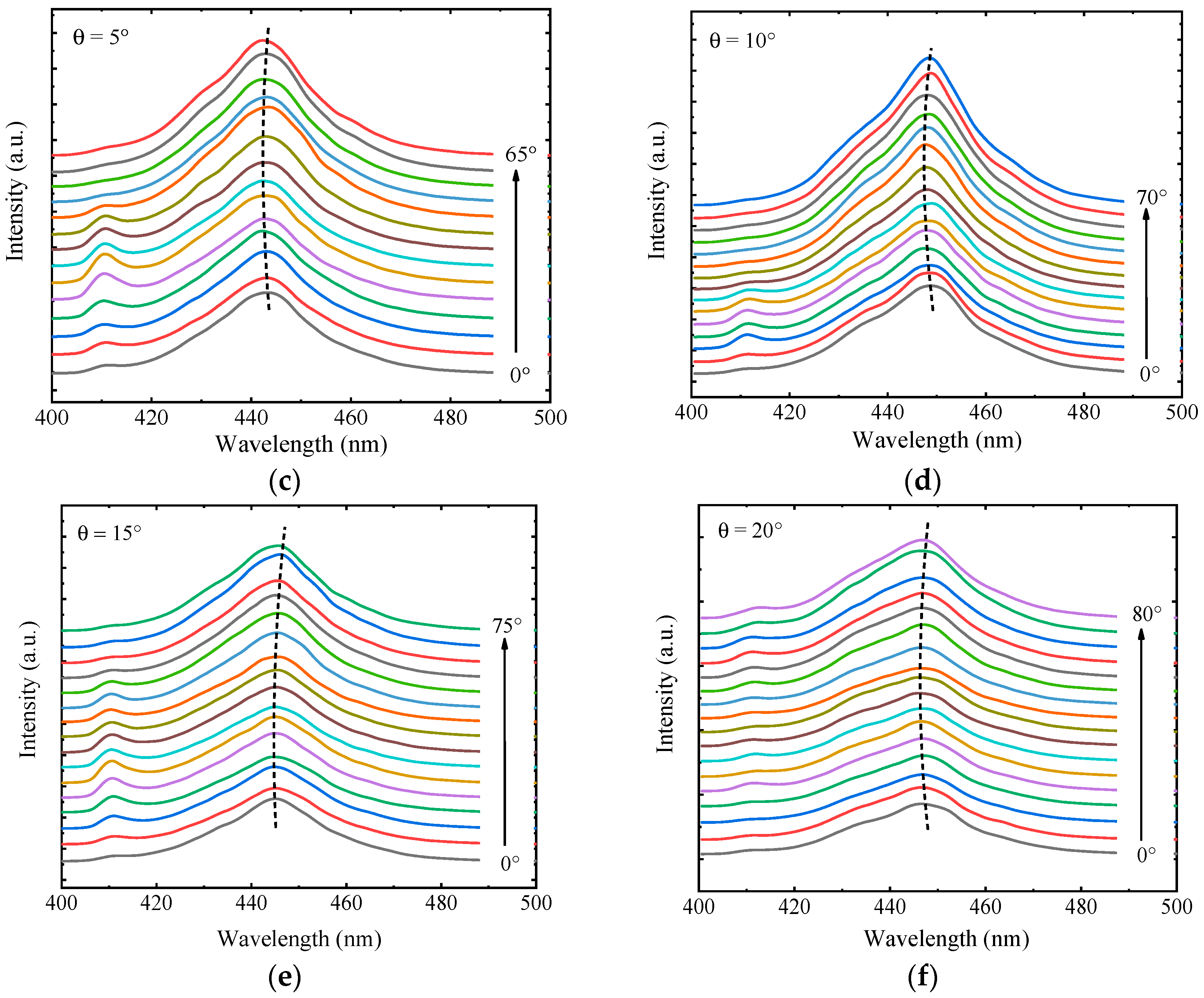
Figure 5b. The “tilt” measurement means that the 0° line passes through the side wall of the triangular ridge, rather than perpendicular to the top surface as usual. We further explored the P450 properties at different tilt angles (θ, 5°~20°), as shown in
Figure 5.
It can be found from
Figure 5 that the peak position shows the same changing trend under all tilt angles (θ = 5~20°), the dash line is an eye-guide line. Although the wavelength shift is smaller than the linewidth at different tilt angles, this does not mean that there is no photon-exciton coupling [
23,
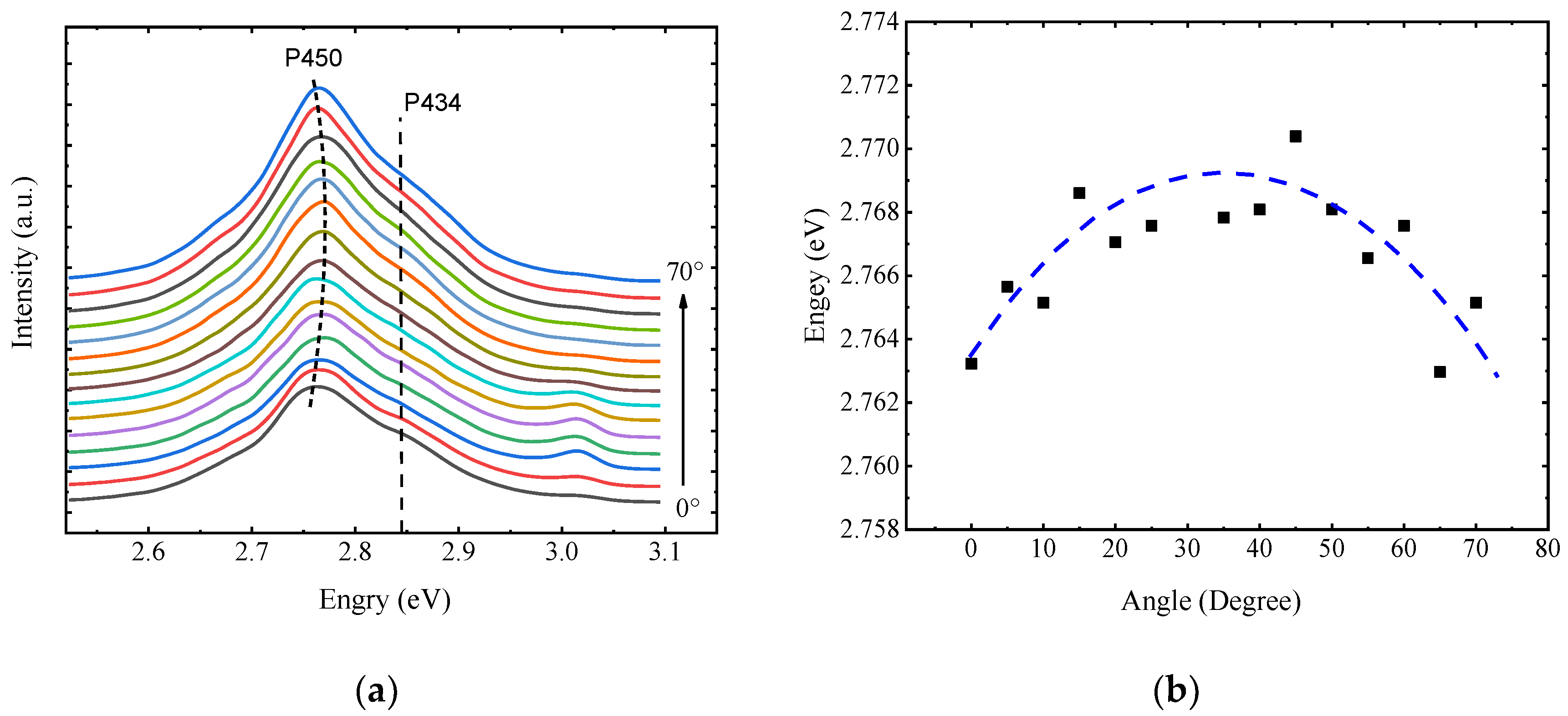
24]. The peak appearing at 410 nm is the emission from the barrier of the MQWs, which is also observable at certain angle during the measurement. At θ = 10°, the peak position changes most obviously. We can obtain
Figure 6a by converting
Figure 5d into photon energy. Obviously, only the peak shift of P450 can be observed. In our AR-PL measurements, a laser spot is large enough to cover the triangular-like ridge, and the MQWs in the ridge is close to the top surface. So, in the measurements, the excitation of the MQWs is almost unchanged, thus the distribution of carriers is unchanged either. Therefore, carrier diffusion has no effect on the shift. We further extracted the peak energy of P450 at different angles through Gaussian fitting, as shown in
Figure 6b. As the angle increases, the peak energy of the P450 moves to a higher energy until about 40°, and then drops to the original energy at about 70°. In InGaN material system, due to the special properties of the material, once the photon cycle occurs, the photons at the high end of the emission spectrum will usually be absorbed. Therefore, when the photon recycling effect is enhanced, the luminous peak will be red-shifted, and the luminous intensity will decrease at the same time. However, none of these are reflected in
Figure 6b, so the photon recycling effect does not show obvious influence on the shift. Since AR-PL measurements are conducted at constant excitation power, the shift cannot be caused by Stark shift and phase space filling. Therefore, the shift of the P450 observed in our experiments is likely caused by coupling with the background light field.
There have been several reports on the exciton–photon coupling in GaN-based microcavities (double DBR planar cavity), and always show the angle-depended PL [
10,
11,
12]. In those cases, the new transition is from the exciton-polariton, and the PL peak energy behaves like a downward arch under different measurement angle. The angle-depended PL behavior is the most important evidence for the formation of exciton-polariton. This judgement can be used for our experiments. The results showed in
Figure 3 and
Figure 6 clear indicate the P450 is from exciton–photon coupling. However, the PL peak energy in our sample behaves like an upward arch under different measurement angle. This can be caused by the different optical modes in different cavities. The ridge cavity clearly has different optical confinement from the double DBR planar cavity.
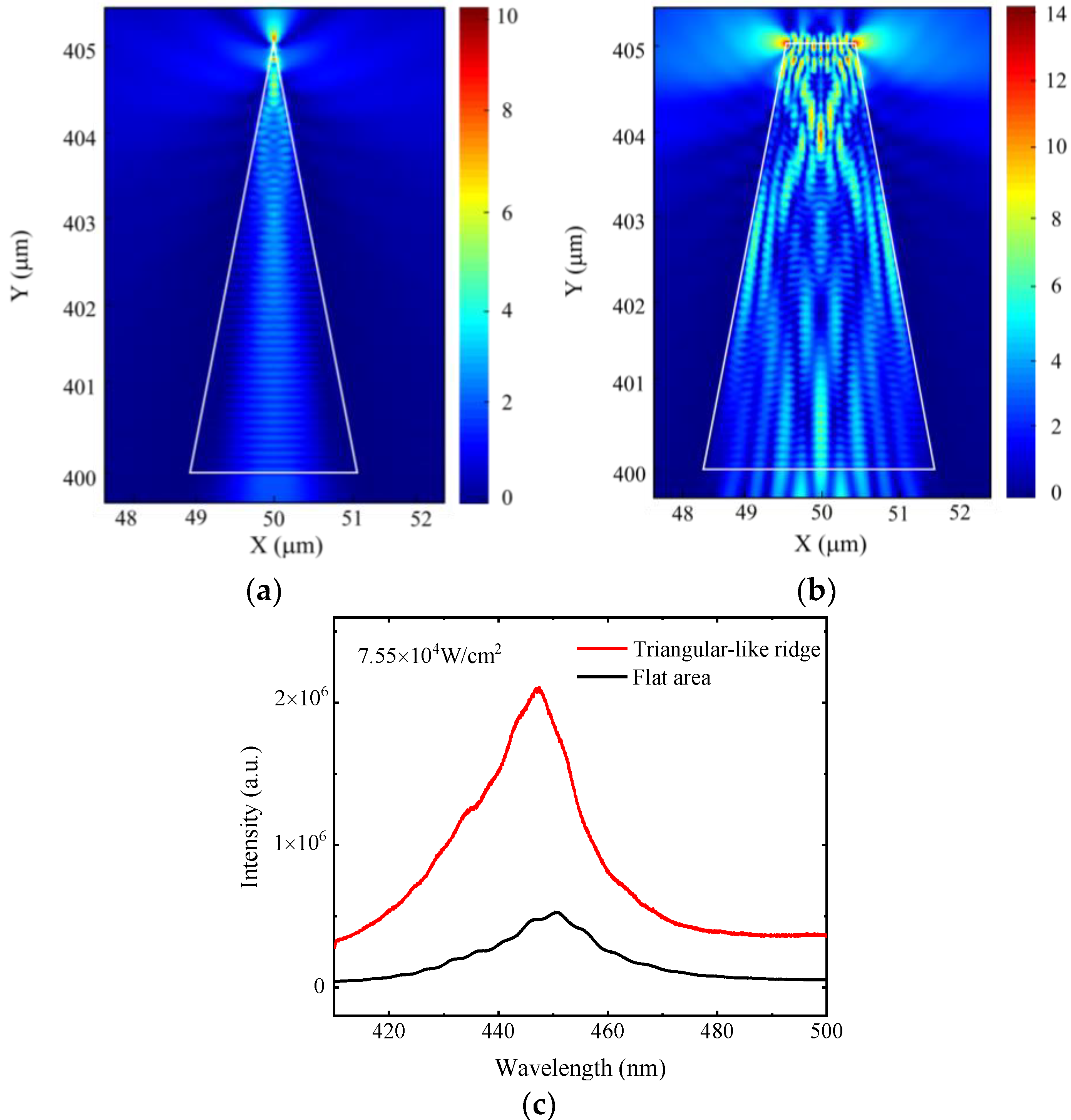
We further use Lumerical’s FDTD Solution software to simulate the optical field distribution in the triangular-like ridge cavity.
Figure 7a,b are the triangular ridge cavities with an apex angle of 26.8°. The vertical axis and horizontal axis of
Figure 7 are the coordinates of the triangular ridge, and the unit is μm. On the right is the electric field intensity bar. The difference between the two structure is that
Figure 7a is an ideal triangular ridge cavity,
Figure 7b is set according to the real sample structure used in our experiment. It can be seen that both the ideal triangular ridge and our actual triangular-like ridge increase spontaneous emission intensity. To more clearly illustrate the enhancement of spontaneous emission by the triangular-like ridge structure, we plot the PL spectra of the flat area and the triangular-like ridge under the same excitation power, as shown in
Figure 7c. In the measurement, the laser spot radius is 500 μm. For our triangular-like ridge, the width of MQWs is 0.9 μm. So we calculate the actual luminous intensity ratio of the triangular-like ridge to the flat area to be 3.5 × 10
3 based on the luminous intensity and effective luminous area of the two samples. The light extraction efficiency is higher than that of the flat area due to the special structure of the ridge. The luminous efficiency of the flat area is 5%, so the light extraction efficiency of the ridge is at most 20 times than that of the flat area. Our actual luminous intensity ratio is 3.5 × 10
3, it is clear that the luminous intensity enhancement of the triangular-like ridge comes from the radiation enhancement. For
Figure 7a, the optical field is mainly concentrated at the top apex, and the internal optical oscillation direction is relatively sample. However, for our actual microcavity
Figure 7b, it is found that the optical field distribution in the ridge is complexed, which complicates the original single oscillation mode. Therefore, at different tilt angles, the incident light will match to a certain oscillation direction, resulting in the weakening or strengthening the coupling of photons and excitons, depending on the intensity of the corresponding optical mode. In addition, since the length of our triangular-like ridge is 1000 μm, the confinement of light in the direction of the ridge is very weak, which is different from the strong confinement of DBR microcavity. So these two factors lead to the coupling of excited states to the optical field rather weak. Anyway, the structural complexity of our triangular-like ridge cavity is much lower than the double DBR cavity reported previously, so if a strong coupling is achieved in the triangular-like ridge cavity, then it is very helpful to achieve device application.


 ,
, 


