
All-Inorganic Perovskite Single Crystals for Optoelectronic Detection


1
Future Energy Laboratory, School of Materials Science and Engineering, Hefei University of Technology, Hefei 230009, China
2
School of Chemistry and Chemical Engineering, Hefei University of Technology, Hefei 230009, China
3
Key Laboratory of Advanced Functional Materials and Devices of Anhui Province, Engineering Research Center of High-Performance Copper Alloy Materials and Processing, Ministry of Education, Hefei University of Technology, Hefei 230009, China
*
Authors to whom correspondence should be addressed.
Crystals 2022, 12(6), 792; https://0-doi-org.brum.beds.ac.uk/10.3390/cryst12060792
Submission received: 12 May 2022
/
Revised: 24 May 2022
/
Accepted: 25 May 2022
/
Published: 31 May 2022
(This article belongs to the Special Issue Progress in Advanced Battery Materials)
Abstract
:Due to their many varieties of excellent optoelectric properties, perovskites have attracted large numbers of researchers in the past few years. For the hybrid perovskites, a long diffusion length, long carrier lifetime, and high μτ product are particularly noticeable. However, some disadvantages, including high toxicity and instability, restrict their further large-scale application. By contrast, all-inorganic perovskites not only have remarkable optoelectric properties but also feature high structure stability due to the lack of organic compositions. Benefiting from these, all-inorganic perovskites have been extensively explored and studied. Compared with the thin film type, all-inorganic perovskite single crystals (PSCs) with fewer grain boundaries and crystalline defects have better optoelectric properties. Nevertheless, it is important to note that only a few reports to date have presented a summary of all-inorganic PSCs. In this review, we firstly make a summary and propose a classification method according to the crystal structure. Then, based on the structure classification, we introduce several representative materials and focus on their corresponding growth methods. Finally, applications for detectors of all-inorganic PSCs are listed and summarized. At the end of the review, based on the current research situation and trends, some perspectives and advice are proposed.
1. Introduction
In the last 10 years, PSCs have attracted large numbers of researchers due to their low defect density, long carrier lifetime, and excellent optoelectronic properties [1,2,3,4,5,6,7]. The chemical formula of perovskite is ABX3 (A = CH3NH3+ (MA) or NH2CHNH3+ (FA), Cs+, B = Pb2+ or Sn2+, and X = Cl−, Br−, or I−). Among them, hybrid organic–inorganic perovskites, represented by MAPbX3 (X = Cl−, Br−, I−) and FAPbX3 (X = Cl−, Br−, I−) [8,9,10,11], have achieved high power conversion efficiency (PCE) in the solar cell. Some solar cells based on the single crystal have also achieved excellent PCEs of 25% or higher [11,12,13,14]. Owing to this, hybrid-type PSCs have also been widely used in the field of detectors, including in X-ray medical detectors [15,16,17], gamma-ray detectors [18], and so on [19,20,21,22,23,24]. Although their noticeable merits have attracted many researchers to study them in depth [3,5,25,26,27] and propose large numbers of improvement methods [28,29,30,31,32], some disadvantages are still inevitable. It has long been thought that the toxicity brought by the lead element and poor stability of perovskite [33,34,35,36] have hindered their broad applications and become the major problems that need to be solved.
Compared with those hybrid perovskites, all-inorganic type perovskites demonstrate better stability in the air [37,38,39,40,41,42,43], and some of them are lead-free [44], which also contain similar merits such as long charge-carrier lifetimes [45], large diffusion length [43], high average atomic numbers, and general tolerance to defects [46]. Benefiting from these remarkable properties, all-inorganic perovskite single crystals, represented by CsPbX3 (X = Cl, Br, I), are becoming promising candidates to develop an optoelectronic device with high and stable performance. Therefore, they have attracted much attention in recent years [47,48,49,50], and to reach higher device performance, more and more scientists have been devoted to the field of improving crystal growth methods [51,52,53,54] and exploring more kinds of new perovskite materials such as low-dimensional materials, double perovskite crystals, and doped perovskite crystals.
Thin films always contain more defects and grain boundaries than those of single crystals [55,56], leading to their worse optoelectric properties. Besides, due to the complex compositions in thin films, the properties of crystals are not easy to be studied and explored, which may hinder the process of their understanding and application. By contrast, single crystals could demonstrate intrinsic properties that are influenced by fewer external factors than thin films. There is no doubt that better growth is a requirement for the generation of single crystals of high quality. To fabricate optoelectronic devices with better performance, optimized growth methods currently still need to be explored and studied in more depth. The growth method is now playing a more and more important role in the fabrication of all-inorganic PSC devices. Nevertheless, there have been few reports about the summary of all-inorganic perovskite single crystal growth methods. Therefore, a systematic summary of the growth and applications of all-inorganic PSCs may help to shed more light on understanding this material system and provide new perspectives to researchers. Since the application of all-inorganic PSCs is mainly focused on the detector field, we mainly introduce its application in the detector in this article.
In this review, firstly, all-inorganic PSCs are divided into several categories according to their structure. Then, based on the classified PSCs, we introduce their corresponding growth methods and related research. Some novel improvements to optimize the growth methods are listed and discussed. Finally, the application of materials in irradiation and photon detectors is discussed in detail. At the end of the review, perspectives and outlooks are proposed based on the current research situation and works.
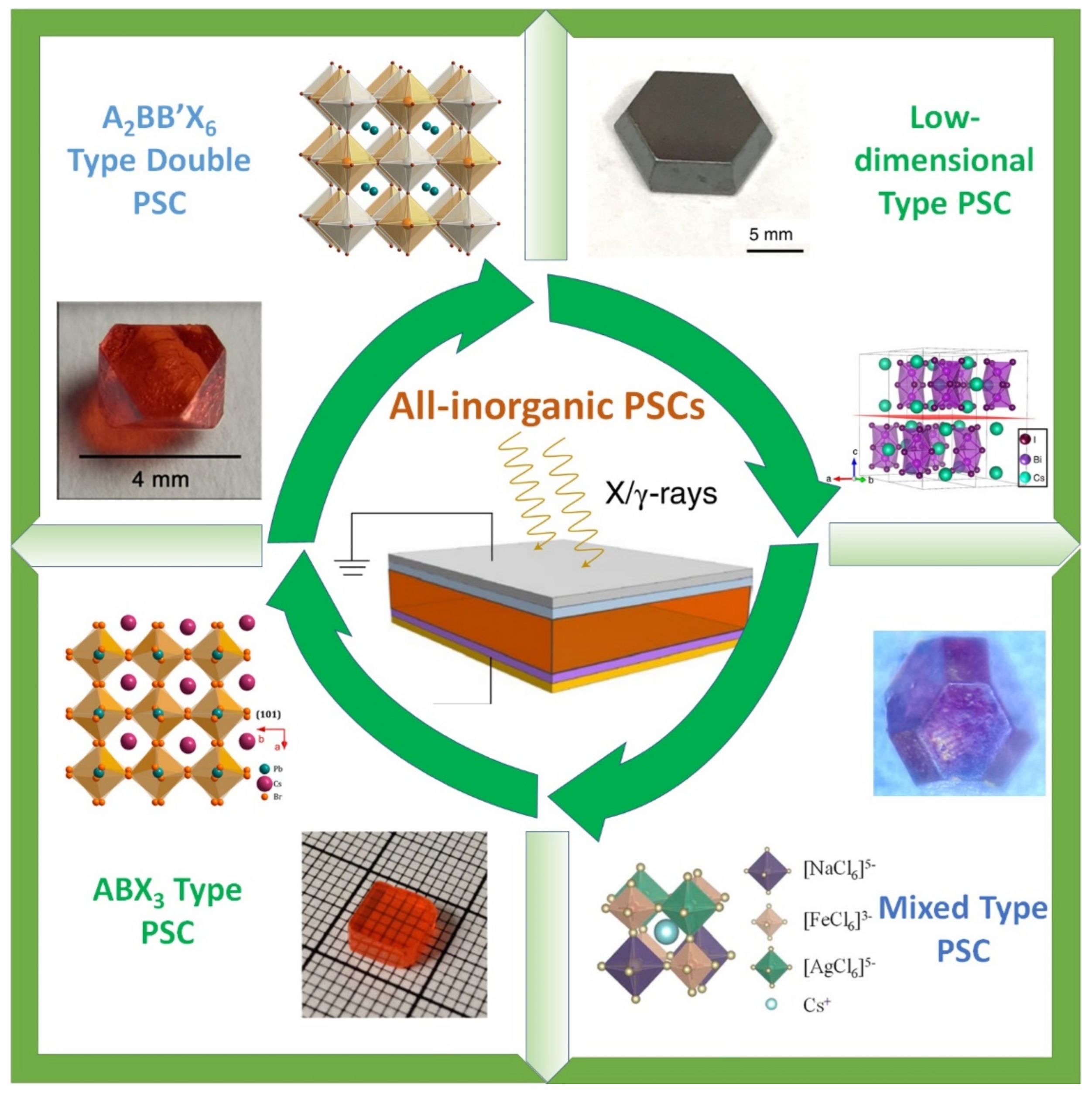
2. Classification of All-Inorganic PSC
It has been thought that the most common formula of perovskite is ABX3, in which A represents an organic or inorganic cation such as MA, FA, or Cs cation, and B represents a Pb or Sn cation. Meanwhile, X represents halogen anions such as Cl, Br, and I. When the perovskite not only contains organic composition at the A site, but also contains inorganic composition at the B site, this kind of perovskite can be categorized as an organic–inorganic hybrid perovskite, represented by MAPbX3. On the contrary, if perovskite does not contain any organic composition, this means that it can be categorized as all-inorganic perovskite.
When the A sites are inorganic ions, this kind of perovskite can be regarded as all-inorganic perovskite; that is, there are no organic compositions in materials, which results in their ultrahigh stability, represented by CsPbBr3.
Apart from the ABX3 conventional type all-inorganic perovskite, other kinds of structures include a double perovskite structure and low-dimensional structure, whose chemical formulas are represented by ABIBIIIX6 and AnBX3+n (n = 3), respectively. All-inorganic perovskites with these novel structures could be made lead-free more easily and also contain larger numbers of attractive merits than the ABX3 type; as a result, they are becoming more and more important in the family of all-inorganic perovskites [57]. Therefore, all-inorganic PSCs with these novel structures are also emphasized in this review.
Except for the pure perovskite mentioned above, some emerging doped PSCs play a crucial role in the family of all-inorganic PSCs [58]. By exploring doped PSCs, we can deeply understand the role of their composition in compounds, which could greatly help researchers to create a systematic PSCs growth theory. Therefore, some doped all-inorganic PSCs are also introduced in this review to thoroughly study the properties of all-inorganic PSCs.
Considering the above-mentioned points, PSCs can be divided into three categories including ABX3 type all-inorganic PSCs, PSCs with special structure, and doped PSCs. Additionally, PSCs with low dimensions and double perovskite PSCs, which belong to the family of PSCs with special structures, are discussed separately. Classification of all-inorganic PSCs is shown in Figure 1. According to the classification, we successively introduce the family of all-inorganic PSCs and their corresponding growth methods.
3. Traditional ABX3 Type All-Inorganic PSCs
The ABX3 type structure is regarded as the representative structure of perovskite. Large numbers of earlier and meaningful reports on perovskite are based on this kind of typical structure. Thus, in the beginning, we introduce the most common type of perovskite and list the progress of crystal growth methods.
3.1. CsPbBr3
All-inorganic perovskite single crystal, CsPbBr3 single crystal (CsPbBr3 SC), was first studied in the 1950s [59]. Currently, CsPbBr3 growth methods can be classified into two kinds of methods: the Bridgman method [60] and the solution-grown method [61]. Based on the Bridgman method, improvement measures have been put forward including optimizing the process parameters and changing the structure of the device, such as in the electrodynamic gradient (EDG) method [52,53]. In terms of solution growth, a large number of optimized growth methods have been proposed by exploring the effect of solution components and optimizing the growth condition and situation. Due to the excellent properties of CsPbBr3, it has adopted the most representative role in the family of all-inorganic perovskite. Therefore, growth methods—especially the Bridgman method and the solution-grown method of the CsPbBr3 PSCs—are summarized in detail first in this review.
I. Bridgman method
As a traditional growth method, the Bridgman method was first proposed by Bridgman in 1925 to grow single crystals of tungsten, zinc, tin, and so on. It is curretnly widely used to grow high-quality and large-size inorganic materials due to its amenability to scale-up and vacuum conditions [62,63]. Benefiting from these merits, the Bridgman method has become a crucial method to grow all-inorganic PSCs.
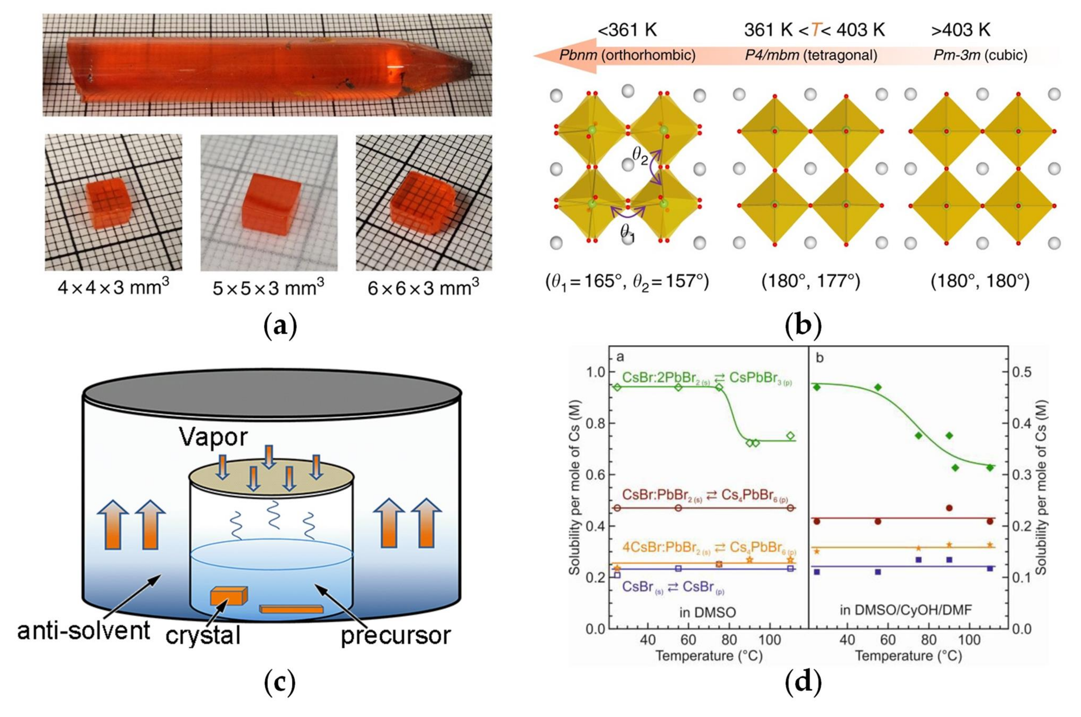
Using the Bridgman method, Stoumpos et al., succeeded in growing CsPbBr3 PSCs with a large size for the first time. They also firstly provided the detailed process of its growth and parameters. Followed by them, He et al. optimized the growth condition based on the relation between the resulting defects and the excessive temperature gradient. After carefully optimizing parameters, CsPbBr3 PSCs of high purity (shown in Figure 2a) were synthesized and showed excellent performance in the gamma-ray detector. They also confirmed that CsPbBr3 exhibits two nondestructive phase transitions at relatively low temperatures. The first phase transition occurs around 130 °C, from a cubic to tetragonal first-order phase transition. This is followed by a second-order transition at around 88 °C to the orthorhombic phase, which is stable at room temperature as shown in Figure 2c [64].
To create a more stable device and avoid the defects caused by the vibration of the growth furnace, Zhang et al., invented the EDG method. Compared with the conventional Bridgman method, mutual movement between the heating device and the ampoule is avoided in the EDG method, whose gradient zone is formed in an adiabatic space and can be precisely controlled by adjusting the temperature of the heating zone and cooling zone. In this case, the temperature gradient can change smoothly, which increases the possibility of obtaining purer crystals in the furnace.
Aiming to explore more state-of-the-art CsPbBr3 growth techniques, some other innovative methods such as the traveling zone melting method [65] have been proposed and must studied further.
Figure 2.
(a) Optical images of Bridgman-grown CsPbBr3 PSCs. Adapted with permission from Ref. [64]. 2018, Springer Nature; (b) phase transition process of CsPbBr3 at different temperature. Adapted with permission from Ref. [64] 2018, Springer Nature; (c) phase transition process of CsPbBr3 at different temperature. Adapted with permission from Ref. [54]. 2017, American Chemical Society; (d) different solubility-temperature profiles in DMSO solvent and DMSO mixed solvent. Adapted with permission from Ref. [66]. 2016, American Chemical Society.

II. Inverse temperature crystallization (ITC) method
In the solution-grown method, precursor solution plays an important part in crystallization. Due to the large difference in solubility among raw materials, the synthesis phase diagram of CsPbBr3 is more complex than that of hybrid perovskite, requiring the careful design of the solvent and stoichiometry to avoid unnecessary phase generation. Saidaminov et al. and Rakita et al. all reported that precursor solution containing 1:1 CsBr and PbBr2 cannot result in perfect CsPbBr3 SCs, and the ratio of raw CsBr and PbBr2 materials needs to be modified [43,61]. After careful analysis, Saidaminov et al. systematically studied this phenomenon and finally designed an optimized ratio of raw materials.
Firstly, due to the limited solubility of N,N-dimethylformamide (DMF), Saidaminov et al. chose dimethyl sulfoxide (DMSO) as the solvent of the precursor solution. When the experiment was carried out using precursor solutions of 1:1 and 1:1.5 CsBr and PbBr2, they found that impurity phase Cs4PbBr6 still dominated the composition of resulting crystals. The reason may be the higher solubility of PbBr2 than that of CsBr. Therefore, when increasing the component of PbBr2 to the 1:2 ratio, the target CsPbBr3 SCs begin to be dominant regardless of some CsPb2Br5. After filtering the solution at 100 °C instead of at room temperature, pure CsPbBr3 SCs are obtained. The detailed results of the experiments are shown in Figure 2e [43]. They confirmed that CsPbBr3 SCs grown by the ITC method have the same bandgap and structure as the crystals grown by the Bridgman-grown method.
Dirin et al., inspired by the solvent used in hybrid PSCs growth, adopted a better solvent containing DMF and γ-butyrolactone, whose solubility–temperature profile (shown in Figure 2b) can be smoother than before [66]. The improved solvent can improve the reproducibility of results and lead to fewer nuclei compared with the former report. Rakita et al. used MeCN and MeOH to decrease the growth temperature in a similar way—after using a two-step heating method, they also finally obtained ideal pure target crystals. As mentioned above, the phase structure of CsPbBr3 PSCs would change when heating. To restrict the phase transition, with the help of choline bromide (CB), Feng et al. developed a growth method and efficiently decreased the growth temperature to 85 °C. Without high growth temperature, defects in crystals were efficiently reduced [67].
III. Anti-solvent vapor-assisted crystallization (AVC) method
Inspired by the AVC method used to grow hybrid PSCs, Rakita et al. firstly reported the solution-grown method to fabricate CsPbBr3 PSCs and made up for the vacancy in the solution growth method [61].
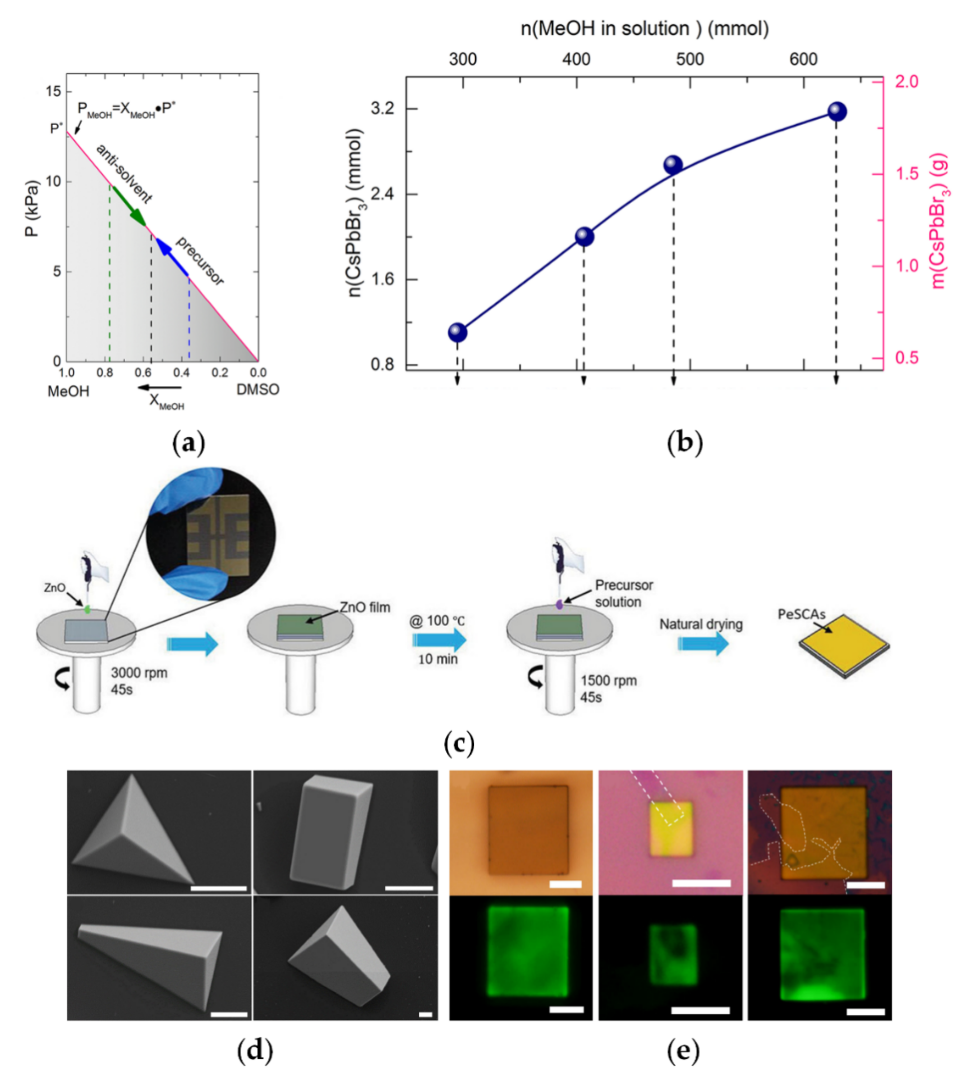
They made a great effort to find a proper anti-solvent to saturate the solution appropriately and solve the problem of the different solubilities between CsBr and PbBr2. Unlike the precursor solution used in the ITC method, in this case, the precursor solution was added with an anti-solvent to make the solution saturated in advance. Then, the solution was put into a container and a balanced antisolvent atmosphere created to diffuse the antisolvent into the growth solution. The scheme of the device is shown in Figure 2d.
To control the growth rate and shed more light on the growth of CsPbBr3 PSCs, Zhang et al. adopted the diluted antisolvent MeOH-DMSO to reduce the vapor pressure of MeOH. They explored the optimized condition that the ratio of PbBr2 and CsBr in the precursor was 1.5:1 and the corresponding mixed antisolvent composition was 50% DMSO and 50% MeOH. Based on this, they obtained the largest CsPbBr3 PSC with a size of 42 × 5 × 3 mm3 of higher quality [54]. Shen et al. thought of CH2Cl2 as an antisolvent for CsPbBr3 and a good solvent for DMF and DMSO [68].
Compared with the ITC method, AVC can efficiently avoid the phase transition during the process of crystallization. At low temperatures, crystals can be more easily grown into a large size. To obtain crystals with large size and high quality, Zhang et al. proposed that three aspects need to be taken into account: the amount of antisolvent vapor diffusion, the concentration of Pb2+ and Br− in precursor solution, and the vapor pressure in a growth environment.
- (1)
- The relationship between the mass of resulting CsPbBr3 and MeOH as the antisolvent volatilized in the precursor solution was explored, and they found that with the increase of antisolvent diffusion, the precipitated crystals also increased (Figure 3b);
- (2)
- The variable mole ratios of PbBr2 and CsBr (n:1) were explored in their work, and they found one metastable region when the value of n was between 1.3 and 1.5. The result shows that in this metastable region, the grown crystals can be changed into white PbBr2·2[(CH3)2SO] after vibration;
- (3)
- The vapor pressure was calculated using Raoult’s law (Figure 3a). Based on the crystals grown at the variable value of XMeOH in the solutions from 100% to 50%, they finally verified that the value of XMeOH should be set at 50% to grow CsPbBr3 PSCs of high quality. From these experiments, it is important to note that these detailed process parameters can greatly influence the growth results and the quality of crystals. Therefore, adopting proper growth conditions should be considered while growing CsPbBr3 PSCs.
In these solution-grown methods, the structure of target crystals always corresponds with the CsPbBr3 PSCs grown by the Bridgman method. Generally, large numbers of features of solution-grown crystals, such as their optoelectric properties, defect density, and resistivity, are comparable with that of CsPbBr3 PSCs grown by the Bridgman method despite there being some differences in detailed parameters.
IV. Other methods
Here, we select several novel growth techniques and introduce them. Tang et al. reported an in-situ growth method to grow CsPbBr3 PSCs onto cubic zinc oxide (c-ZnO), thus producing perovskite single-crystal arrays (PeSCAs). This invention can be used as an inorganic electron transport layer in optoelectronic devices. They observed that the (100) plane of cubic CsPbBr3 and the (100) plane of c-ZnO can match properly in the lattice distance, enabling the growth of PeSCAs via the spin-coating method (shown in Figure 3c) [69].
It is worth mentioning that the epitaxial growth of PSCs on c-ZnO is better than on a substrate without c-ZnO. XRD patterns show the appearance of impurities (Cs4PbBr6) when the epitaxial growth is carried out without c-ZnO. Obtained single crystals with epitaxial growth demonstrated high purity and quality, leading to a faster diffusion rate than nanocrystals, which also showed the superior stability of the optical properties and structure.
Wang et al. reported a CVD method to create CsPbX3 SCs including CsPbBr3, CsPbI3, and CsPbCl3 [70]. Compared with the in situ grown methods, the CVD method needs vacuum conditions, thus greatly avoiding unintended impurity introduction. Therefore, crystals grown by the CVD method generally exhibit a smooth surface and are free of apparent grain boundaries (shown in Figure 3d). Under a broad field UV excitation, the CsPbCl3, CsPbBr3, and CsPbI3 platelets clearly showed uniform blue, green, and red emissions inside the platelets, as shown in Figure 3e, suggesting highly uniform optical properties throughout the entire platelet.
Figure 3.
(a) The calculation result of vapor pressure using Raoult’s law Adapted with permission from Ref. [54]. 2017, American Chemical Society; (b) relationship between the obtained mass of CsPbBr3 and the amount of MeOH in solution. Adapted with permission from Ref. [54]. 2017, American Chemical Society; (c) schematic of the preparation of PeSCAs, with the inset showing the substrates used in the experiments Adapted with permission from Ref. [69]. 2020, John Wiley and Sons; (d) SEM images of CVD-synthesized CsPbX3 PSCs Adapted with permission from Ref. [70]. 2016, Springer Nature.; (e) emissions of CsPbX3 PSCs under UV excitation Adapted with permission from Ref. [70]. 2016, Springer Nature.

To enhance the stability of CsPbX3 PSCs, Zheng et al. proposed a CsPbI3@SiO2 nanocomposite system, namely confining the CsPbI3 into SiO2 [51]. This measure aimed to improve the stability of photoluminescence performance. Testing results indicated that CsPbI3@SiO2 could retain 95% of its initial PL intensity, while the bulk CsPbI3 type only retains 30%. From this perspective, the stability of PSCs can be enhanced by modifying the whole material system other than some traditional detailed growth conditions.
3.2. TlPbI3
TlPbI3 features high stability in air and excellent optoelectric properties, like CsPbBr3. It has been explored since the 2000s [71,72] and has demonstrated good potential in the field of detectors. Due to its low melting temperature, thermally activated defects could be effectively reduced during the process of growth. Considering this merit, researchers always adopt the Bridgman method to grow TlPbI3 PSCs.
M. Kocsis first synthesized TlPbI3 using the heating method and firstly applied it to X-ray detectors [72]. However, the resulting crystal from the heating method is a polycrystal instead of a single crystal. To overcome the boundaries in the pristine growth samples, Khyzhun et al. adopted the Bridgman method to grow high-quality single crystals with TlI and PbI2 as raw materials. After direct melting and growth in the Bridgman device, a high-quality crystal was obtained [73].
Recently, Hany et al. managed to grow TlPbI3 PSCs with the optimized Bridgman method and fabricated gamma-ray detectors with them. They systematically studied the properties and structure of TlPbI3 [74]. Via a temperature-dependent IV measurement, they also calculated a high resistivity of about 2 × 10¹¹ Ω cm at room temperature, which was beneficial to minimize noise and increase resolution. Despite TlPbI3 PSCs featuring many advantages including high resistivity, large bandgap, long charge carrier drift length, and excellent stability, compared with the μτ product of other all-inorganic PSCs, charge carrier transport properties of TlPbI3 still need to be further improved to satisfy the basic criteria of detectors.
3.3. CsSnI3
Chung et al. first studied the overall properties of CsSnI3 including conductivity, carrier concentration, hole mobility, and so on by using experimental methods and theoretical calculations [75]. In their work, they used the Bridgman method to obtain high-quality CsSnI3 SCs. P-type metallic behavior of CsSnI3 was verified, and they found that this kind of new material has the highest hole mobility among the p-type semiconductors. Due to the remarkable intrinsic properties, they further applied doped CsSnI3 to solar cells and created all-solid-state dye-sensitized solar cells with remarkable performance, whose PCE reached 10.2% [76]. Though solar cells were fabricated by using the CsSnI3-containing solution, CsSnI3 SCs with remarkable intrinsic optoelectric properties should be studied in more devices.
Wu et al. adopted the calculation method to investigate CsSnI3 and predicted the 23% PCE for optimized CsSnI3 PSCs solar cells. They also studied the difference between SCs and polycrystalline, verifying that PSCs have better properties than polycrystals [77]. Despite CsSnI3 PSCs having remarkable properties [78] and the notion that they could be promising candidates to replace toxic CsPbBr3, current research on CsSnI3 mainly focuses on solar cells fabricated by the solution-grown method [77,79]. Therefore, CsSnI3 PSCs solar cells still need to be explored and studied further. Other emerging ABX3 type all-inorganic perovskites such as TlHgBr3 [80,81] and CsGeX3 [82,83] are not discussed here because of their limitations regarding toxicity or growth methods.
4. All-Inorganic PSCs with Low Dimensions
The general formula of perovskites can be described as AnBX2+n; when n = 1, this kind of ABX3 type perovskite, as mentioned above, is referred to as a 3D perovskite, and when n = 4, the A4BX6 type perovskite would be referred to as a 0D perovskite because under this circumstance the BX64− octahedral in perovskite forms isolated dots. When the dimensions of crystals reduce, the photoluminescence quantum yield (PLQY) increases [84,85,86,87], based on which researchers try to study the 0D materials to achieve quantum confinement and high PLQY. Other materials with low dimensions such as A3B2X9 type PSCs could also exhibit unique advantages [85]. Therefore, in this section, we introduce some PSCs with low dimensions, especially A3B2X9 and A4BX6 type PSCs.
4.1. A3B2X9 Type PSC: Cs3Bi2X9 (X = Br or I), Rb3Bi2I9 and (NH4)3X2I9 (X = Sb or Bi)
Due to the high toxicity in traditional CsPbBr3 PSCs, researchers have come up with large numbers of methods to replace the lead element in CsPbBr3. The most popular way now is to replace Pb with some non-toxic elements such as Sn, Ge, and Bi. Among them, Bi-based perovskite is regarded as a promising candidate to solve this problem because it not only has numerous similarities compared with Pb-based PSCs but also is environmentally friendly.
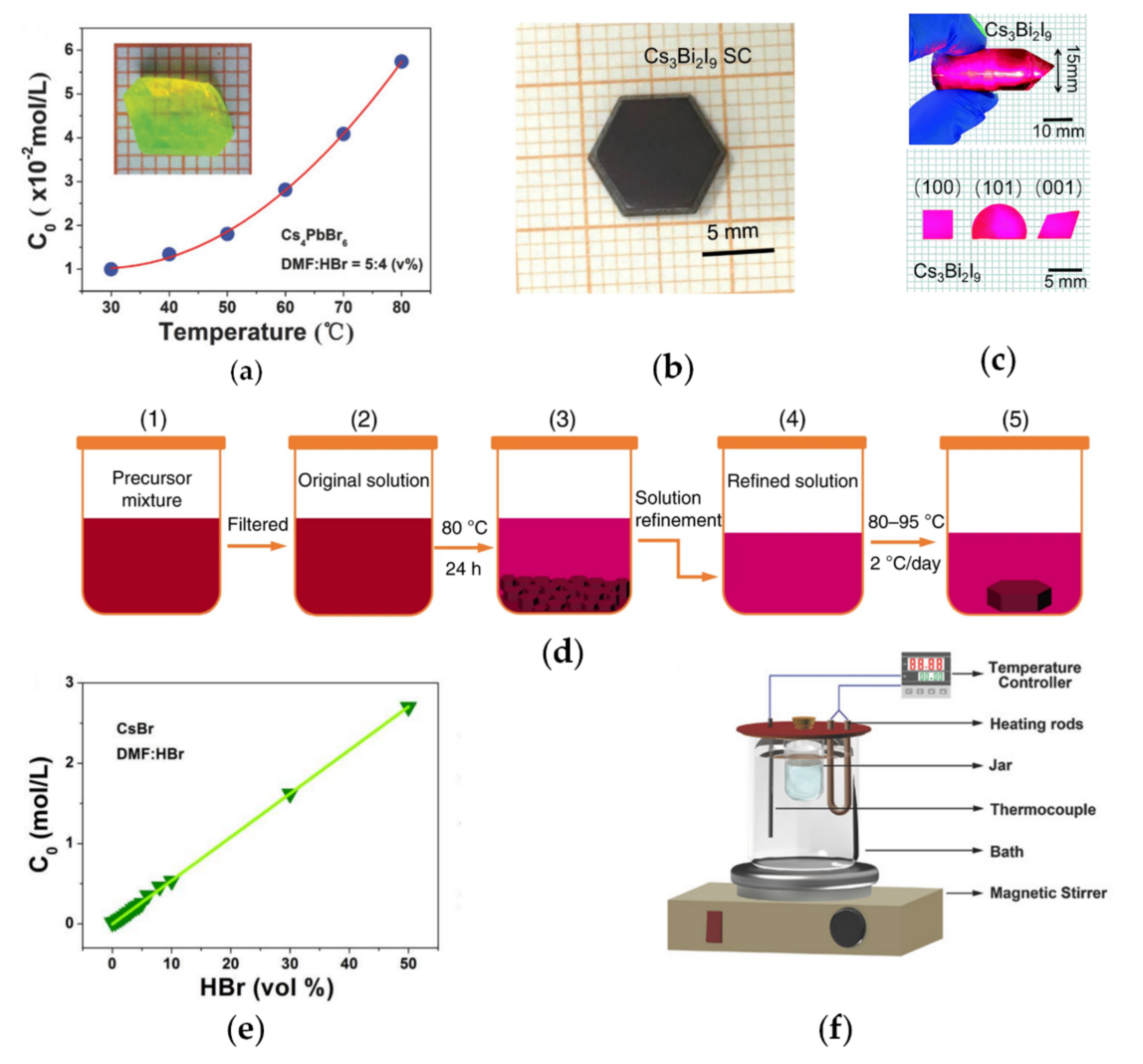
Sun et al. adopted a modified vertical Bridgman method to grow 0D Cs3Bi2I9 SCs of high quality [88]. The optical image is shown in Figure 4c. After analyzing the optical and electrical anisotropic properties of this kind of 0D Cs3Bi2I9, they reported the first observation of resolved energy peaks using alpha particles with an excellent spectral resolution of 32%. Also with the Bridgman method, Li et al., synthesized larger Cs3Bi2Br9 PSCs and first applied them to X-ray detectors, which demonstrated the great potential in the field of X-ray detectors [89].
Recently, Zhang et al. proposed a novel solution-grown method that could effectively control the crystal nuclei in the solution, further improving the efficiency of single-crystal growth [90]. Based on the classical nucleation theory, when there are crystal sites with a radius (r) larger than the critical nucleation radius r0 (r > r0), they will grow spontaneously into bigger crystallites or precipitates, which could greatly hinder the growth of single crystals. However, once the extra nuclei are removed by refining the solution, single crystals will easily be grown. According to this, Cs3Bi2Br9 PSCs with large sizes were synthesized (shown in Figure 4b). The diagram of the process is shown in Figure 4d.
Figure 4.
(a) Photograph of a grown embedded crystal and the Cs4PbBr6 solubility curve. Adapted with permission from Ref. [91]. 2018, John Wiley and Sons; (b) optical image of Cs3Bi2I9 PSC grown by a nuclei-control method. Adapted with permission from Ref. [90]. 2020, Springer Nature; (c) photographs of Cs3Bi2I9 PSCs grown by the Bridgman method Adapted with permission from Ref. [88]. 2018, Royal Society of Chemistry; (d) diagram of nuclei-control growth process. Adapted with permission from Ref. [90]. 2020, Springer Nature; (e) with the increase of HBr content in DMF solution, the solubility of CsBr also increased Adapted with permission from Ref. [91]. 2018, John Wiley and Sons; (f) diagram of SCM crystal growth set up Adapted with permission from Ref. [91]. 2018, John Wiley and Sons.

Xia et al. systematically studied the structural descriptor for A3B2X9 PSCs and synthesized 2D Rb3Bi2I9 using the controlled cooling solution-grown method [92]. The 2D Rb3Bi2I9 was verified to have high X-ray attenuation coefficients, and the assembled X-ray detector reached a record low detection limit among all perovskite X-ray detectors, also exhibiting better stability than a detector made from traditional CsPbBr3 PSCs.
While the toxicity caused by the lead element in perovskite should be taken seriously, the toxicity of some typical solvents such as DMF and DMSO should also be carefully considered. These two solvents could easily be absorbed by the human body. Considering this, Zuo et al. proposed the (NH4)3Sb2IxBr9-x PSCs family, which could be grown without DMF or DMSO as a solvent [93]. They adopted ethanol as the solvent to dissolve the raw materials NH4I and SbI3. By using the AVC method, they finally grew (NH4)3Sb2I9 PSCs with a hole mobility of 4.8 cm2 V−1 s−1 and electron mobility of 12.3 cm2 V−1 s−1. Zhuang et al., designed (NH4)3Bi2I9 PSC X-ray detectors with an extremely low detection limit [94]. They also validated that (NH4)3Bi2I9 PSCs would be easily scaled up within the AVC method, the hole and electron μτ products of which are comparable with μτ products of hybrid type MAPbBr3 PSCs. In the growth process of (NH4)3Bi2I9 PSCs, DMF is replaced with hydroiodic acid as a solvent. High quality, reduced toxicity in the process, and low cost are their features, which would enable (NH4)3X2I9 PSCs (X = Sb or Bi) to have a great potential in other application fields.
In short, because of the excellent properties of A3B2X9 type low-dimensional PSCs, especially their non-toxic characteristics, they are attracting more and more researchers and have been regarded as promising candidates to produce environmentally friendly devices with high performance.
4.2. A4BX6 type PSC: Cs4PbBr6 and Cs4EuX6(X = Br, I)
As mentioned above, the growth of CsPbBr3 PSCs in solution cannot be easily controlled due to the appearance of side products such as Cs4PbBr6. Saidaminov et al. studied this phenomenon and used the different solubilities between them when synthesizing 0D Cs4PbBr6 crystals that demonstrated high PLQY and remarkable optical properties [85]. Cha et al. adopted the AVC method to grow 0D Cs4PbBr6 and 3D CsPbBr3 crystals under different growth environments [84] and, after comparison, they proved the 0D Cs4PbBr6 had a large exciting binding energy which could lead to poor performance in photodetectors.
The above-mentioned 0D Cs4PbBr6 crystals are small in size because these solution-grown methods are mainly suitable for the growth of 3D CsPbBr3 instead of 0D Cs4PbBr6. Chen et al. proposed the slow cooling method (SCM) to control the process of crystal growth and, using this method [91], centimeter-sized 0D Cs4PbBr6 PSCs with embedded 3D nano CsPbBr3 crystals were successfully grown.
SCM is a simple and versatile technique for solution crystal growth via controlling solubility. In this method, the precursor solution should be saturated in advance; then the crystal seed can be put into the cooling solution, and the crystal seed would grow upward in the solution. The setup for crystal growth is shown in Figure 4f. To obtain 0D Cs4PbBr6 PSCs from the solution, they introduced HBr as an additive to increase the solubility of CsBr. Meanwhile, they found that HBr is beneficial to decreasing the PbBr2 DMF intermediates, thus boosting the crystallization process. With the SCM method and HBr additive, centimeter-sized single crystals of high quality were grown. They finally fabricated high efficiency (151 lm W−1) and 90.6% color gamut prototype WLED devices using 0D Cs4PbBr6 PSCs.
Wu et al. first reported 0D-halide-perovskite-based scintillators that demonstrated a high gamma-ray detection efficiency using Cs4EuX6 (X = Br, I) PSCs grown by the vertical Bridgman method [95]. This kind of special 0D structure with strongly localized excitons is beneficial to achieving high scintillation efficiency. the scintillation yield significantly increases with the reduction of the perovskite dimension (shown in Figure 5d), which suggests that the 0D structure with strongly localized excitons is beneficial for achieving high scintillation efficiency. The dominant factor non-proportionality (nPR) in determining the energy resolution of these two crystals is shown in Figure 5c. The ideal nPR response will be the same number of photons emitted per energy unit for any given gamma-ray energy. It is noticeable that, compared with NaI:Tl, Cs4EuX6 has less deviation, with decreasing gamma-ray energy demonstrating better proportionality.
These reports show that these kinds of all-inorganic 0D A4BX6 type perovskites have high radiation detection efficiency and high PLQY, providing one way to fabricate detectors and luminescent devices with high performance.
4.3. Copper Type Low-Dimensional PSC: Cs3Cu2I5
As mentioned above, perovskite with a 0D structure has the potential to achieve high scintillation efficiency. Since its excellent properties are reported, other kinds of new 0D PSCs have been explored and studied. Recently, Lin et al. synthesized Cs3Cu2I5 PSCs with an ultrahigh photoluminescence quantum yield (PLQY~100%) using the AVC method [96].
They observed dual self-trapped exciton (STE) emissions in Cs3Cu2I5, which showed a strong electron–phonon coupling. Results of temperature-dependent PL spectra and Raman spectra demonstrate the thermal-assisted radiative recombination of dark STEs, which could provide special insight into the application of high-quantum-efficiency light-emitting devices.
Cheng et al. adopted the Bridgman method to grow Cs3Cu2I5 bulk single crystals. Crystals grown in this way were more transparent and purer [97]. They confirmed that the Cs3Cu2I5 crystal not only demonstrates a high scintillation yield and an extremely low afterglow under X-ray radiation but also possesses a high light yield under γ-ray radiation.
These excellent properties (high PLQY, high scintillation yield, low afterglow, and remarkable energy resolution) enable Cs3Cu2I5 SCs to become promising alternatives in the field of radiation detection.
4.4. Heterometallic Type Low Dimensional PSC: Cs4MnBi2Cl12
Cs4MnBi2Cl12 features a triple-layered two-dimensional structure (shown in Figure 5a). Wei et al. [98] managed to synthesize Cs4MnBi2Cl12 PSCs with a solution-grown method. Like other all-inorganic PSCs, Cs4MnBi2Cl12 PSCs have strong soft X-ray attenuation and bright radiative luminescence under X-ray irradiation.
Figure 5.
(a) The triple-layered two-dimensional structure diagram of Cs4MnBi2Cl12. Adapted with permission from Ref. [98]. 2020, Elsevier; (b) crystal structure diagram of Cs4EuX6, where the purple polyhedral represents the tilted and isolated EuX64− octahedral, and green and purple ellipsoids represent Cs and X atoms. Adapted with permission from Ref. [95]. 2018, Royal Society of Chemistry; (c) dominant factor of Cs4EuI6 and Cs4EuBr6 Adapted with permission from Ref. [95]. 2018, Royal Society of Chemistry; (d) relationship between the dimension and scintillation light yield in CsnEuI2+n family. Adapted with permission from Ref. [95]. 2018, Royal Society of Chemistry; (e) patterned fish-like images and QR code of Cs4MnBi2Cl12 under (left) visible and (right) UV light, respectively. Adapted with permission from Ref. [98]. 2020, Elsevier.

They first studied the PLQY of Mn+ doped CsMnCl3 and found the PLQY was very low. Then, doping with another metal, Bi, resulted in Cs4MnBi2Cl12 PSCs exhibiting remarkable orange emission with a high PLQY of 25.7%. They proposed the reason for the increase in PLQY to be the exciton transfer process from the [BiCl6]3− octahedron to [MnCl6]4− octahedron. In this process, the transformation increased the exciton density in 4T1g, thus boosting the PLQY. After blending PSC powder with commercial phosphors, they obtained efficient white emission under the excitation of a 365 nm UV chip. Besides, by filling Cs4MnBi2Cl12 powders into designed patterned grooves, delicate images such as fishes and QR codes (shown in Figure 5e) were presented, suggesting their prospects as high-resolution PL imaging agents. They also tested Cs4MnBi2Cl12 PSCs’ potential in X-ray detectors and, with a commercial digital camera, they fabricated an efficient detection device. The target object was recognized with the help of their invented detection devices.
5. All-Inorganic A2BB′X6 Type PSCs
Except for exploring new elements to replace toxic Pb ions in CsPbBr3, as mentioned above, many researchers have made a great effort to find perovskite with new structures to avoid the appearance of the Pb element. For instance, double perovskite with a special structure could offer two B site atoms per unit. Some other combination of atoms may be more stable than two Pb atoms. Therefore, in this section, we introduce some emerging materials with novel double perovskite A2BB′X6 structures.
5.1. Cs2AgBiBr6
Inspired by the oxide double perovskites A2BB′O6, Slavney et al. first managed to grow Cs2AgBiBr6 PSCs and studied their potential in optoelectric applications [99]. Using the ITC method and making some improvements including thermal annealing and surface treatment, they managed to grow high-quality Cs2AgBiBr6 crystals (shown in Figure 6a). Zhang et al. synthesized Cs2AgBiBr6 PSCs with a large size using precursor solution with the addition of 30% CH3COONa [100]. After surface treatment and thermal annealing, Cs2AgBiBr6 PSCs were verified to be effective to improve X-ray detection in detectors.
Yin et al. developed a controlled cooling method to grow Cs2AgBiBr6 PSCs; compared with other normal ITC methods, this could effectively improve the efficiency of single-crystal growth [101]. In the beginning, they systematically studied the relationship between nucleation and concentration (shown in Figure 6e); in the light of the above relationship, after carefully setting the growth environment, especially the cooling process, they obtained high-quality Cs2AgBiBr6 PSCs and managed to avoid the appearance of extra crystal seeds.
Slavney et al. proved that Cs2AgBiBr6 has a long photoluminescence (PL) lifetime and an indirect bandgap of 1.95 eV [99] suited for a tandem solar cell. They also carried out experiments to verify that the stability of solution-grown Cs2AgBiBr6 PSCs was higher than that of hybrid organic-inorganic type PSCs. XRD patterns in Figure 6b suggest that Cs2AgBiBr6 PSCs would maintain their pristine structure after long-term exposure to the environment. By contrast, XRD patterns of hybrid type would change slightly after treatment. Their remarkable stability, without doubt, makes them more promising in applications.
5.2. Cs2InAgCl6
As mentioned above, the band structure of Cs2AgBiBr6 is indirect, which could lead to a limitation on optoelectric applications. To explore more double perovskite-type candidates in the photovoltaic field, Volonakis et al. calculated the properties of Cs2InAgCl6 and fabricated Cs2InAgCl6 PSCs with a solution-grown method, whose crystal structure is shown in Figure 6c [102]. Cs2InAgCl6 PSCs with a direct band-structure, without doubt, are more fit for optoelectronic devices. Besides, they confirmed the good stability of Cs2InAgCl6 PSCs, and it is possible to form Cs2InAg(Cl1−xBrx)6 for x < 1. A tunable band-gap was also achieved by adopting the composition of doped materials.
Luo et al. successfully fabricated stable UV photodetectors with Cs2InAgCl6 PSCs [103]. Cs2InAgCl6 PSCs of high quality with an ultra-low trap-state density ((8.6 ± 1.9) × 108 cm−3) were synthesized by taking a one-pot hydrothermal method. Oxygen was found effective for controlling Cs2InAgCl6 PSCs’ surface composition, thus influencing their optical properties. They also verified that after UV-O3 treatment, the photoconductivity and on–off ratio of detectors can be improved a great deal. As shown in Figure 6d, it is noticeable that detectors with treated Cs2InAgCl6 PSCs demonstrated better photoconductivity. Finally, fabricated devices were proved to effectively harvest UV signals, whose detectivity and on–off ratios reached 1012 Jones and 500, respectively.
Other novel all-inorganic double PSCs, such as Cs2TlBiI6 [104], Cs2AgxNa1-xFeCl6 [105], and so on, are also experimentally explored or calculated by various methods; nevertheless, here, we mainly introduce the synthesized PSCs with a specific application, so we do not introduce these materials in detail. In terms of lead-free characteristics and optoelectrical properties, these A2BB′X6 type double PSCs could be promising candidates to be further applied, and there is no doubt that they should be explored further.
Figure 6.
(a) The optical image of Cs2AgBiBr6 PSC. Adapted with permission from Ref. [99]. 2016, American Chemical Society; (b) XRD patterns of Cs2AgBiBr6 after long-term exposure to environment. Adapted with permission from Ref. [99]. 2016, American Chemical Society; (c) structure diagram of Cs2InAgCl6. Adapted with permission from Ref. [103]. 2018, American Chemical Society; (d) photoconductivity test of Cs2InAgCl6 PSC under different conditions. Adapted with permission from Ref. [103]. 2018, American Chemical Society; (e) solubility and saturation curves of Cs2AgBiBr6 crystal at different temperatures. Adapted with permission from Ref. [101]. 2019, John Wiley and Sons.

6. Mixed Type All-Inorganic PSCs
To further improve the properties and quality of all-inorganic PSCs, more and more researchers have been devoted to doping other kinds of elements in these PSCs. Mixed type PSCs are not only able to reduce the amount of Pb element in materials but also to boost their properties [106,107]. In the field of ABX3 type perovskite, the stability of their structure can be represented by the tolerance factor (τ), which can be calculated via the following Equation (1):
where rA, rB, and rX represent the ion radii of A, B, and X, respectively. Generally, when the τ of the PSC structure is in the range of 0.77 to 1.10, the PSC structure is considered as structurally stable. In theory, doping an external element would change the τ of the structure, thus affecting the stability. Many experimental studies on doped materials verified that, with the extra composition introduction, the pristine structure stability and optical properties are indeed enhanced. Given their special merits, these mixed-type all-inorganic PSCs enriched varieties of traditional ABX3 type materials. Here, for the sake of comprehensiveness, we introduce research works that include all three sites (A, B, X site) of ion mixed type materials.
6.1. CsPbIxBr3−x (0 < x < 3)
Yang et al. adopted the ITC method to prepare iodine-mixed CsPbBrxI3-x PSCs by adjusting the amount of PbBr2 and PbI2 [108]. They found that, with the increase of iodine content, impurities brought by the growth environment can be reduced and the thermal stability of PSCs can be enhanced, which indicated that mixing some other elements into the material is also a good choice to broaden the research ideas and improve the devices’ performance.
Zhao et al. explored the CsPbIxBr3−x crystal anisotropy effect of materials on optical and electrical properties [109] with the first-principle calculation and drift-diffusion model to find a class of proper mixed CsPbIxBr3−x material and a suitable crystal orientation to achieve a high PCE in the solar cell. After calculating the effect mass, deformation potential, and elastic moduli in different orientations, they found that the obvious anisotropy effect in the crystal led both the electron and hole mobility along [001] to be far higher than those along [100]. Based on this phenomenon, they adopted different device structures and drift-diffusion models to predict the PCE of devices. After utilizing CsPbIBr2/silicon and CsPbI2Br/silicon tandem structures along the [001] orientation, much higher PCEs were achieved up to 26.32% and 31.39%, respectively. To date, solar cells fabricated by thin-film CsPbIxBr3−x reached 20.1% PCE [110], which means that CsPbIBr2 solar cells should be explored further. Jia et al. discussed the influence factor of CsPbIxBr3−x solar cells in detail [111]. To obtain better CsPbIxBr3−x solar cells, numerous improvements still need to be proposed regarding defect passivation, crystallization, and so on. There is still a long way to go to achieve a better CsPbIxBr3−x PSC application. Meanwhile, the authors emphasized that the excellent thermal stability of these PCEs would make them competitive candidates in solar cells.
Although Zhao et al. only carried out theoretical calculations, the study of anisotropy is meaningful in the scope of single crystals, and their related calculation results are helpful to further applications, especially for solar cells. These above-mentioned research works demonstrate that when applying PSCs to optoelectronic devices, orientation and doped elements could also be important factors that need to be carefully considered.
6.2. CsPb1-xBixBr3 (0 < x < 1)
To reduce the amount of toxic Pb ions in traditional CsPbBr3 SCs, Miao et al. chose the Bi element to develop Bi-doped CsPb1-xBixBr3 PSCs [112]. They found that with an increase of the Bi component, absorption was slightly improved and the absorption spectra of Bi-doped PSCs could cover entirely the visible spectrum. Besides, it is noteworthy that although the introduction of trivalent Bi element slightly increases the defect density of the crystal, the carrier concentration of the crystal will increase a great deal; combined with the ideal absorption spectra, CsPb1-xBixBr3 PSCs are suitable for further optoelectric applications. As shown in Figure 7b, the dielectric constant test result also suggests their better ion mobility.
Doping external element generally needs growth optimization to obtain correct crystals. For Bi-doped CsPb1-xBixBr3 PSCs, they adopted a modified AVC method to grow PSCs (shown in Figure 7e). They first used the controlled cooling method to foster prime crystal seeds; after filtration, these crystal seeds with the saturated solution were then put into the AVC growth setup to allow the crystal seeds to grow. Benefiting from the solution-grown method, they could easily adapt the molar ratio of raw materials PbBr2 and BiBr3 in precursor solution, thus controlling the compositions of ultimate crystals.
They also verified the photostrictive effect of CsPb1-xBixBr3 PSCs, which could expand the scope of CsPb1-xBixBr3 applications, such as in microactuators and microsensing.
Figure 7.
(a) With the doping of atoms, the size and structure of crystal cells change. Adapted with permission from Ref. [113]. 2019, American Chemical Society; (b) capacitance test results of CsPbBr3 and CsPbxBi1−xBr3 single crystals at different frequencies. Adapted with permission from Ref. [112]. 2017, Royal Society of Chemistry; total absorption spectra (c) and PL spectra (d) of Cs1−xRbxSnBr3 samples with 0 ≤ x ≤ 0.3. Adapted with permission from Ref. [113]. 2019, American Chemical Society; (e) schematic diagram of the modified AVC method. Adapted with permission from Ref. [112]. 2017, Royal Society of Chemistry.

6.3. Cs1−xRbxSnBr3 (0 < x < 1)
Currently, to enhance the stabilization of PSCs and their relative devices, the strategy of doping multiple cations in the A site has proven to be feasible. Inspired by this thought, Bernasconi et al. systematically studied the Cs1−xRbxSnBr3 PSCs system to find if there is a way to solve the instability of pure CsSnBr3 roused by the oxidation of Sn2+ to Sn4+ in the air. They successfully synthesized Cs1−xRbxSnBr3 PSCs with the high-temperature melt growth method [113]. In this work, the influence brought by the doped Rb element on the crystals’ stability, properties, and structure was emphasized.
They found that, after doping Rb ions into PSCs, the tolerance factor of crystals was increased, leading to higher stability. At the same time, the cell volume of Cs1−xRbxSnBr3 PSC decrease with the Rb content doping (Figure 7a). The absorption spectra and photoluminescence (PL) spectra also slightly shifted when changing the composition (shown in Figure 7c,d, respectively). Furthermore, it is noteworthy that an increase in charge carrier lifetime is induced by the Rb inclusion. With higher stability and better properties, these positive results verified that Cs1−xRbxSnBr3 SCs have great potential in the field of optoelectronic devices, which also indeed indicated the feasibility of doping external elements.
With the doping method, many excellent devices and materials were invented; for example, Chung et al. doped SnF2 into CsSnI3 to fabricate devices with a high PCE, and Bernasconi et al. doped the Rb element into CsSnBr3 to obtain more stable and excellent crystals. Some researchers have also developed Ge-doped, Mn-doped, and Ag mixed perovskites aiming to remove some limitations on traditional PSCs. These mixed-type materials greatly enrich the family of all-inorganic PSCs and also provide more research areas to scientists. Combined with the convenience brought by the solution-grown method, mixed type all-inorganic PSCs still have great potential and should be explored further.
7. Applications and Properties
The high average atomic numbers, long carrier lifetimes, high mobility, and ultra-high stability of all-inorganic PSCs mean that their applications cover many categories. Benefiting from remarkable properties, all-inorganic PSCs have received broad attention for applications in optoelectronic devices. In the above part of the article, we focus on the growth methods of different kinds of all-inorganic PSCs and the corresponding application direction. Detailed parameters of devices and their properties are not mentioned.
In this section, we introduce the applications and properties of all-inorganic PSCs in three main fields: gamma-ray detectors, X-ray detectors, and photon detectors. In addition, some devices made up of polycrystalline thin films and hybrid organic–inorganic perovskites are also listed to shed more light on the difference between all-inorganic PSCs and other perovskite structures.
7.1. Carrier Mobility and Lifetime
To systematically introduce the detector applications and their properties, in this part, we firstly introduce the two important carrier properties of semiconductors, mobility and lifetime, with their measurement methods. For one semiconductor detector, the type of transport carrier can be determined by selecting the electrode. The LUMO and HOMO level of the semiconductor and the work function of the electrode are key parameters affecting the carrier transport. These energy level differences would lead to different energy barriers for electrons and holes. Therefore, by utilizing the different energy barriers for electrons and holes, hole-only and electron-only devices can be fabricated, respectively. For instance, if the work function of the electrode is near the LUMO level of the semiconductor, electrons would be difficult to transfer to the HOMO level, thus resulting in a high energy barrier for electrons, based on which the hole-only device can be determined; vice versa, the electron-only device can also be determined in the same way. After determining the type of transmission carrier, further carrier property measurement can be carried out.
For typical semiconductor detectors, space charge limited current (SCLC) technology could measure the trap density and the carrier mobility of semiconductors. This kind of I–V measurement is of importance to understanding the internal mechanism. Generally, with the increase of bias voltage, the device would first demonstrate the Ohmic properties, and the current is proportional to the voltage. In the next region, the current would sharply be increased at the VTFL point, which is the trap-filling process, and in the last region, the relation between the current and the voltage would be in line with the following Equation (2) (known as Mott–Gurney’s law):
In which J and V are current density and voltage, respectively; L is the sample thickness; ε and ε0 are relative permittivity and vacuum permittivity, respectively; and μ is the mobility. Therefore, with this equation, mobility can be calculated in I–V measurement. The trap density can also be indicated by the VTFL point. It can be calculated with Equation (3):
Figure 8i is the measurement results of the I–V test with the corresponding schematic diagram of three different stages [114]. Except for the SCLC method, other characterization methods such as time of flight (TOF) and Hall effect measurement are also able to demonstrate the carrier mobility; to date, numbers of measurement methods have been widely used. However, there are still some errors in the data from different research groups. A more accurate method still needs to be invented.
Carrier lifetime is also one important property of materials indicating the carrier transport ability. Thus, here, we introduce a representative measurement of it: the time-resolution photoluminescence spectrum (TRPM). When nonequilibrium carriers are generated in semiconductors, they will be affected by impurities and defects, and then hole carrier recombination will occur. When photogenerated carriers are generated in the material, Equation (4), as follows, is used:
where N(t) represents the number of photogenerated carriers at time t, and τ is the carrier lifetime. TRPM technology utilizes this principle to detect the photoluminescence intensity decay phenomenon, thus indirectly calculating the carrier lifetime. The intensity decay pattern would be fitted by the following Equation (5) [115]:
where I(t) is the decay intensity; A1 and A2 are the decay amplitude; and τ1 and τ2 are taken from the recombination of surface traps and body defects, respectively. After the pattern is fitted, the final carrier lifetime can be calculated from Equation (6):
Apart from the above-mentioned two properties that can indicate the carrier transport capability, other parameters such as diffusion length and effective mass are also important for materials and detectors. However, given that the mobility and the carrier lifetime are used most widely and with these two properties, other properties such as diffusion length can also be easily obtained, we do not introduce other properties for semiconductors here.
7.2. X-ray Detectors
The X-ray wavelength ranges from 0.001 nm to 10 nm, featuring high frequency, large energy, and excellent penetration ability. X-ray detection is of great importance to medical imaging, the nondestructive inspection of luggage nuclear power stations, and scientific research [116,117,118]. Traditional materials used in X-ray detectors represented by CdZnTe and CdTe could meet the basic needs of X-ray detection in most cases [119,120]. Three key parameters—the atomic number, μτ product, and resistivity of materials—that greatly affect the performance of X-ray detectors should be carefully considered [90]. Compared with the emerging perovskite materials, the μτ product of traditional materials is lower [66], and the resolution and performance of devices made of CZT still need to be further improved. For example, devices with a low detection limit allow the human body to receive less X-ray radiation in medical imaging, which is crucial to improving the safety of medical treatment. Given the great importance of X-ray detection, better detection materials need to be explored further.
X-ray detectors can be categorized into two types: (1) scintillator type and (2) semiconductor type [121]. Nevertheless, the former type of detector features a lower energy resolution and a more complex system configuration. This is because scintillator-type detectors need an extra component: a photomultiplier tube. When the scintillator type detector is irradiated by an X-ray, its scintillator would firstly accumulate X-ray energy. Then, the electron would be activated and escape from the scintillator. These electrons would next get into the photomultiplier tube to generate much more electrons, thus boosting the signal in the detection system, which requires many components to work together and obviously leads to a complicated system.
By contrast, semiconductor type detectors with a simple structure can directly convert an X-ray to a current signal, as shown in Figure 8b,g, which makes them more suitable for the following high-resolution digital analysis. Here, we list some detailed properties and mainly introduce some detectors based on semiconductors (shown in Table 1) to systematically analyze the all-inorganic PSCs. To understand the X-ray detectors overall, we first introduce some of their basic characteristics here.
First of all, sensitivity plays an important role in the characterization of device performance, which shows, how much signal was produced when the detector was irradiated by an X-ray—namely, the current generated. This value (S) can be described with Equation (7):
where A is the area of detectors exposed to the X-ray; D is the dose rate of the X-ray; I and Idark are the measurement current under an X-ray and in the dark, respectively. This is a general indicator for detectors that is also suitable for X-ray detection.
Another important characterization of X-ray detectors is the low detection limit. As mentioned above, the lower the detection limit, the fewer X-rays would need to be used in daily life. The low detection limit calculation method can be traced back to Currie’s work in 1968 [122]. Currently, according to the rule defined by the IUPAC (International Union of Pure and Applied Chemistry), the detection limit is set to the corresponding X-ray dose when the response signal becomes three times the noise signal (diagram shown in Figure 8j) [123]. Note that this definition factually may not be suitable for every situation, Pan et al. proposed an updated statistical method to expand and improve upon the previous formula, which has better accuracy.
In Table 1, we list the properties of crystals and their corresponding growth methods. Key parameters of X-ray detectors, low detection limit and sensitivity, and the structure of the detector are also listed. From this table, we could notice that detectors made of hybrid PSCs demonstrate ultrahigh sensitivity whether in thin films or PSCs; therefore, in terms of sensitivity and their instability, hybrid PSCs are suited for short-time applications that require very high sensitivity, such as in outer space or on the moon. For all-inorganic materials, their high stability and low detection limit make them suited for large-scale medical testing. Given that some of them are non-toxic, they are more suitable for wide application in medical devices, which could relieve environmental pressure.
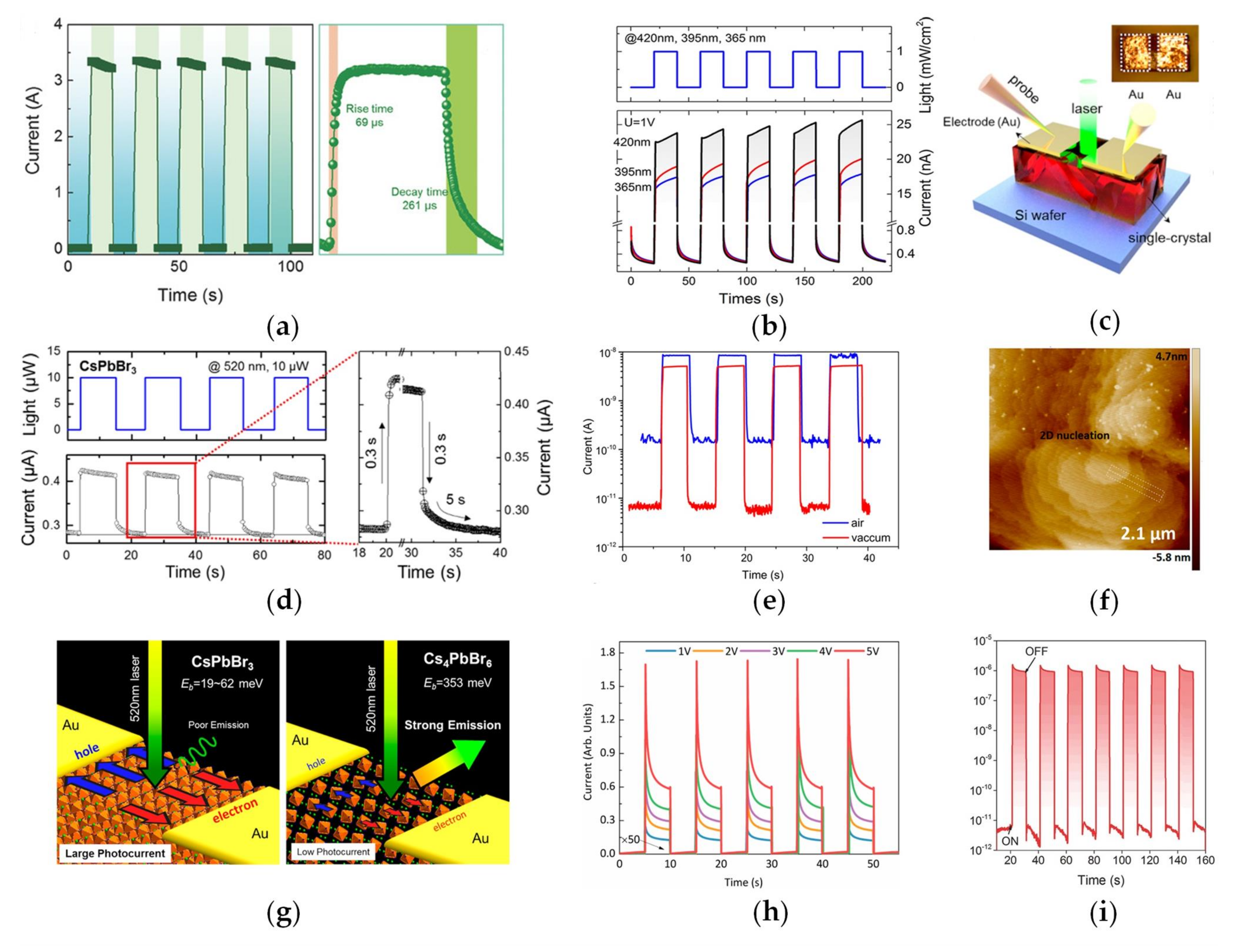
Improvements in crystal growth greatly affect the performance of devices. Zhang et al. confirmed that by adopting the solution-control method, Cs3Bi2I9 PSCs with better quality and a larger size could be achieved. They subsequently fabricated devices with the structure shown in Figure 8b, whose actual detection experiments and absorption coefficients comparison are shown in Figure 8a,c, respectively. Additionally, Pan et al. adopted thermal annealing and surface treatment to obtain Cs2AgBiBr6 PSCs of better quality, whose attenuation efficiency is shown in Figure 8f. As shown in Figure 8d,e, the dark current and responsivity of devices are greatly optimized due to these crystal treatments. Combined with the high attenuation efficiency, Cs2AgBiBr6 PSCs are now attractive materials in the field of X-ray detection. With the modified Bridgman method, Li et al. invented Cs3Bi2Br9 X-ray detectors that verified their excellent time-responding capability. Utilizing the detector structure shown in Figure 8g, Steele et al. also tested temperature-dependent X-ray detection performance. They found that with the temperature decrease, more current was generated (as shown in Figure 8h) and the rise time was delayed because of their lower carrier mobility, which was helpful to understand their long-term detection performance. Note that adopting some properly improved methods and treatments is of great importance to fabricated devices.
Apart from devices based on semiconductors, scintillators could also be used to detect X-rays. Mykhaylyk [124] and Cheng [97] reported the application of an X−ray scintillator with CsPbBr3 PSCs and Cs3Cu2I5 PSCs, respectively. For scintillators, their scintillation is a crucial parameter that could indicate the quality of the device. The scintillation light yield of CsPbBr3 at 7 K is assessed to be 50,000 ± 10,000 ph/MeV at excitation with 12 keV X−rays, and the Cs3Cu2I5 crystal demonstrates a high scintillation yield of about 32,000 photons MeV−1, which means that all-inorganic PSCs are promising materials for scintillator-type X-ray detection and should be explored further to enrich the family of X-ray detection.

Table 1.
Detailed information about the applications of X-ray detectors.
| Materials | Growth | μτ Product (cm2 V−1) | Resistivity (Ω cm) | Structure of Detectors | Electrical Field (V mm−1) | Sensitivity (µC Gyair−1 cm−2) | Low Detection Limit (nGyair s−1) | Reference |
|---|---|---|---|---|---|---|---|---|
| CdTe | Modified directed crystallization | 1.5 × 10⁻⁴ | 108–109 | Diode structure | * 90 V | 1.2 | - | [125] |
| α-Se | - | 10−7 | - | α-Se/ (α-Si:H) TFT | 15,000 | 0.44 | - | [126] |
| Cs2AgBiBr6 PSC | ITC method | 6.3 × 10⁻³ | 1.6 × 10¹¹ | Au/CABB /Au | 25 | 105 | 59.7 under 5 V | [114] |
| Cs2AgBiBr6 PSC | ITC method | - | - | Ag/CABB/Ag | 6 | 316 | 91.98 under 1 V | [121] |
| Cs2AgBiBr6 PSC | ITC method | 2.48 × 10⁻³ | 5.4 × 10⁹ | Au/CABB /Au | - | - | - | [127] |
| CsPbBr3 PSC | ITC method | - | − | Ag/CPB/ITO | 8 V * | 770 | - | [128] |
| CsPbI3 (1D) PSC | ITC method | 3.63 × 10⁻³ | 7.4 × 10⁹ | Au/CPI/Au | 4.17 | 2370 | - | [129] |
| Rb3Bi2I9 PSC | ITC method | 2.51 × 10⁻³ | 2.3 × 10⁹ | Au/RBI/Au | 300 | 159.7 | 8.32 under 1 V | [92] |
| Cs3Bi2I9 PSC | ITC method | 7.97 × 10⁻⁴ | 2.79 × 10¹⁰ | Au/CBI/Au | 50 | 1652.3 | 130 under 50 V mm−1 | [90] |
| Cs3Bi2I9 PSC | Bridgman method | 6.10 | 1012 | Au/CBI/Au | 450 | 111.9 | - | [88] |
| Cs3Bi2Br9 PSC | Bridgman method | 3.73 × 10⁻⁵ | 6.8 × 10¹¹ | Au/CBB/Au | 200 V * | 230.4 | - | [89] |
| MAPbBr3 PSC | AVC method | 4 × 10⁻³ | - | Si-integrated device | 7 V * | 21,000 | 36 under 1 V | [130] |
| MAPbBr3 PSC | AVC method | 1.2 × 10⁻² | 1.7 × 10⁷ | Au/MPB/C60/BCP/Au | - | 80 | 500 under 0.1 V | [16] |
| MAPbI3 thin film | Spin-coating method | 2 × 10⁻⁷ | - | Ag/ZnO/PCBM/MPI/PEDOT:PSS/ITO/Glass | 1300 | 2.5 × 10⁴ µC Gyair−1 cm−3 * | - | [131] |
| MAPbI3 thin film | Spin-coating method | 10−4 | - | ITO/PI-MPI/MPC/PI-MPI/TFT | 240 | 11,000 | - | [15] |
| MAPbI3 wafer | Nanocrystalline compression method | 2 × 10⁻⁴ | - | ITO/PMMA/MPI/Au | 200 | 2527 | - | [132] |
| (NH4)3Bi2I9 PSC | ITC method | 1.1 × 10⁻² | − | Ag/NHBI/Ag | 6.5 | 803 | 55 under 6.5 V mm−1 | [94] |
* unit is different from the corresponding table title.
Figure 8.
(a) X-ray image of key and nut obtained from the Cs3Bi2I9 PSC detector. Adapted with permission from Ref. [90]. 2020, Springer Nature; (b) schematic of the Cs3Bi2I9 PSC-based X-ray detector structure. Adapted with permission from Ref. [90]. 2020, Springer Nature; (c) absorption coefficients of Cs3Bi2I9 and other materials. Adapted with permission from Ref. [90]. 2020, Springer Nature; (d,e) comparative measurements of resistivity and responsivity of devices made of the pristine crystal and treated crystal. Adapted with permission from Ref. [114]. 2017, Springer Nature; (f) relationship between attenuation efficiency and thickness of 50 keV X-ray photons in several typical semiconductors. Adapted with permission from Ref. [114]. 2017, Springer Nature; (g) photograph of fabricated detectors based on Cs2AgBiBr6 PSC. Adapted with permission from Ref. [133]. 2018, John Wiley and Sons; (h) measurement results of photocurrent response of the detector to 61.12 μGy S−1 X-ray at different temperatures. Adapted with permission from Ref. [133]. 2018, John Wiley and Sons; (i) measurement results of I−V test with the corresponding schematic diagram of different stages. Adapted with permission from Ref. [114]. 2017, Springer Nature; (j) diagram explanation of detection limit. Adapted with permission from Ref. [123]. 2021, Springer Nature.

7.3. Gamma-Ray Detectors
Similar to X-ray detectors, gamma-ray detectors can also be divided into two categories: devices based on (1) scintillators and (2) semiconductors. Gamma rays feature a very large energy and a wavelength even shorter than that of X-rays. Gamma-ray detection has played an important part in many areas including security imaging, nuclear inspection, medical treatment, and some basic scientific research [134,135].
An average atomic number, μτ product, and resistivity are also three basic requirements for gamma-ray detection materials. Traditional zinc-alloyed CdTe single crystals possess high resistivity and a large μτ product, so they have been widely used in many gamma-ray detectors [136]. Nevertheless, the cost-restricted crystal manufacturing at a scaled-up level and low hole mobility of traditional CZT crystals have hindered the development of CZT gamma-ray detectors. Compared with traditional CZT single crystals, PSCs feature low-cost, high mobility, and are easy to grow; because of this, many scientists have come up with many methods to apply this kind of emerging PSCs to gamma-ray detectors and have fabricated devices with high performance. Here, we list detailed information including the growth, device structure, semiconductor properties, and energy resolution under different test sources. This information on all-inorganic PSC gamma-ray detectors is shown in Table 2.
To better understand the application of gamma-ray detectors, we introduce the energy resolution concept of gamma-ray detectors. Under the irradiation of gamma rays with different energy, an energy-resolved gamma-radiation spectrum could be obtained. Near the energy peak of the spectra, half of the response peak could be recognized at two points. The energy difference between two points would be the full width at half maxima (FWHM); then, the energy resolution could be calculated with Equation (8):
where ER is the energy resolution and Emax is the energy value of the peak point. This resolution value could reflect the gamma-ray detection capability and the responsivity of the device.
From Table 2, compared with hybrid organic–inorganic PSCs, all-inorganic PSCs demonstrate better performance in gamma-ray detectors with generally higher energy resolution. He et al. reported detectors with 1.4% energy resolution made of CsPbBr3 PSCs grown by the Bridgman method [45]. In addition, the stability of all-inorganic PSCs is much better than that of hybrid PSCs, and they are easy to grow on a large scale using the Bridgman method. Detectors made of all-inorganic PSCs also demonstrate better performance than that of the hybrid type. Therefore, there is no doubt that all-inorganic PSCs could be more ideal materials in the field of gamma-ray detectors than hybrid organic–inorganic perovskites.
Meanwhile, in general, all-inorganic CsPbBr3 PSCs grown by the Bridgman method possess a better μτ product and higher energy resolution than CsPbBr3 grown by the ITC method, which also confirms the superiority of the Bridgman method. Therefore, in terms of crystal growth, vacuum condition and the lack of extra composition boost the crystallization process in the Bridgman method. Hence, the easy scaling-up and crystals of high quality grown by the Bridgman method effectively promote the progress of the development of detectors.
Due to their high PLQY characteristics, the low-dimensional PSCs in Table 2 also demonstrate significant performance in scintillator-based detectors, which also means that low-dimensional PSCs have great potential in the field of gamma-ray detection. Since there are few reports on low-dimensional PSC and double perovskite-type PSC used in gamma-ray detectors, it is worthwhile to pay more attention to the development of environment-friendly and excellent gamma-ray low-dimensional type and double type PSC detectors. The multiple choices of the elements in these materials makes this goal more possible.
Table 2.
Detailed information about the applications of gamma-ray detect.
| Materials | Growth | μτ Product (cm2 V−1) | Resistivity (Ω cm) | Structure of Detectors | Test Source | Energy Resolution | Reference |
|---|---|---|---|---|---|---|---|
| CZT | Traveling heater method | 1.5 × 10⁻² | - | - | 122 keV 57Co | 3.0% | [137] |
| 662 keV 137Cs | 0.91% | ||||||
| CZT | Bridgman method | 1.3 × 10⁻³ | 2.2 × 10¹⁰ | - | 88 keV 109Cd | 3.7% | [138] |
| 59.5 keV 241Am | 4.9% | ||||||
| Cs4EuI6 PSC | Bridgman method | - | - | Scintillator | 662 keV 137Cs | 5.0% | [95] |
| Cs4EuBr6 PSC | Bridgman method | - | - | Scintillator | 662 keV 137Cs | 4.3% | [95] |
| CsPbBr3 PSC | ITC method | 4 × 10⁻⁴ | - | Ga/CPB/Au | 662 keV 137Cs | 5.5% | [139] |
| 122 keV 57Co | 13.1% | ||||||
| 59.5 keV 241Am | 28.3% | ||||||
| CsPbBr3 PSC | ITC method | 1.34 × 10⁻³ | - | Ga/CPB/Au | 662 keV 137Cs | 5.5% | [67] |
| CsPbBr3 PSC | ITC method | 2 × 10⁻⁴ | 3 × 10⁹ | - | 59.5 keV 241Am | - | [66] |
| CsPbBr3 PSC | Bridgman method | 1.34 × 10⁻³ | - | Ga/CPB/Au | 122 keV 57Co | 3.8% | [64] |
| 662 keV 137Cs | 3.9% | ||||||
| CsPbBr3 PSC | Bridgman method | 8 × 10⁻³ | >109 | EGaIn/CPB/Au | 662 keV 137Cs | 1.4% | [45] |
| TlPbI3 PSC | Bridgman method | 3.43 × 10⁻⁵ | 2 × 10¹¹ | Ag/TPI/Ag | - | - | [74] |
| Cs3Cu2I5 PSC | Bridgman method | - | - | Scintillator | 662 keV 137Cs | 3.4% | [97] |
| Bi-poor Cs2AgBiBr6 PSC | ITC method | 1.47 × 10⁻³ | 1.56 × 10¹¹ | carbon /CABB/carbon | 59.5 keV 241Am | 13.91% | [140] |
| MAPbI3 PSC | ITC method | 8 × 10⁻⁴ | - | Ga/MPI/Au | 59.5 keV 241Am | 12% | [18] |
| 122 keV 57Co | 6.8% | ||||||
| FAPbI3 PSC | ITC method | 10−2 | - | - | 59.5 keV 241Am | 35% | [141] |
| MAPbBr2.94Cl0.06 PSC | ITC method | 1.8 × 10⁻² | 3.6 × 10⁹ | Cr/MAPBC/C60/bathocuproine /Cr | 662 keV 137Cs | 6.5% | [142] |
| MAPbBr2.85Cl0.15 PSC | ITC method | - | 2.57 × 10⁸ | Cr/MPBC/Cr | 662 keV 137Cs | 25% | [143] |
| 59.5 keV 241Am | 35% |
7.4. Photodetectors
Photodetectors play an important role in image sensing, location tracking, and basic scientific research [2,144]. Owing to the excellent optoelectric properties of PSCs, they recently have received much attention in the field of photodetectors, represented by hybrid organic–inorganic MAPbBr3 PSCs. Currently, researchers are trying to optimize hybrid PSCs to overcome their instability in many ways, such as doping other elements, surface passivation, and so on. However, a perfect stabilization method is still lacking. By contrast, in photodetectors, all-inorganic PSCs not only have remarkable optoelectric properties but also have higher stability and a longer life span. Therefore, in this part, we introduce the current research on the application of photodetectors based on all-inorganic PSCs.
To better understand the research on photodetectors, we first introduce some key parameters. The following three parameters are widely used to indicate the performance of detectors, which could reflect the detection capability and responsivity to light.
- (1)
- Responsivity:The responsivity calculation formula is as above (Equation (9)), where I is the actual current generated under the light conditions; Idark refers to the dark current generated without light; P in the denominator is the power intensity of the incident light; and S refers to the area irradiated by the light, which is the area of the exposed perovskite crystal in this device. Responsivity could reflect the intensity of the generated signal under light, which could indicate the detection performance and efficiency of detectors.
- (2)
- External quantum efficiency (EQE):The EQE calculation formula is as above (Equation (10)), where R is the responsivity shown in Equation (9); λ is the wavelength of light; e and c are electron charge and the velocity of light, respectively. The EQE value represents the ratio between the number of electrons generated by the incident light and the number of photons irradiated on the effective working area of the photodetector in unit time, which could indicate the photon–electron conversion efficiency.
- (3)
- Detectivity:where ∆f is the electric bandwidth and in represents the background noise current. This value could indicate the lowest intensity of light that could be recognized from the noise signal. This value also has great reference significance in practical application. To manifest the actual performance in application, apart from these three key parameters that should be calculated and considered, an I-t test could also demonstrate the comparison between the light-on and light-off situation. The on–off ratio and its time-dependence would overall reflect the practical detection performance. Considering this, the on–off ratio test is also of significance to the detector test.
In the above part, we introduce some key values of detectors. Here, we introduce the detector performance with the corresponding growth method. Utilizing the Bridgman method, Song et al. synthesized ultra-large CsPbBr3 PSCs with excellent carrier mobility and fabricated dual-modal photodetectors. The testing results showed that CsPbBr3 PSCs have excellent electrical transporting properties, and the fabricated devices also demonstrated good detection performance under 532 nm lamination (shown in Figure 9a). For solution-grown CsPbBr3 PSCs, Dirin et al. utilized them to fabricate photodetectors, whose spectral responsivity under 10 V-bias shows a very sharp (∼20 nm FWHM, centered at 550 nm) peak demonstrating a responsivity of 6 A/W [66]. The μτ product is measured to be 2 × 10⁻⁴ cm2 V−1, which is lower than that of Bridgman-grown CsPbBr3 SCs because of the inclusions brought from the environment. Although the μτ product of solution-grown crystals is generally smaller, they are also able to achieve high performance in detectors. Saidaminov et al., using CsPbBr3 PSCs grown by the ITC method, successfully fabricated detectors with an ultrahigh 105 on–off ratio, and their low dark current was verified (shown in Figure 9i) [43].
To reduce the inclusions in crystals and optimize the growth process, many researchers have made a great effort in improving growth conditions and revealing growth mechanisms. Zhang et al., using the improved solution-grown method, successfully synthesized centimeter-sized crystals and fabricated photodetectors with a strong response to optical light (shown in Figure 9b) [54]. Ding et al. revealed that the growth of CsPbBr3 PSCs corresponds to a 2D nucleation mechanism (shown in Figure 9f) and reported photodetectors with a responsivity of 0.028 A/W and a response time of <100 ms, whose on–off test result is shown in Figure 9h [145].
For low-dimensional SCs, Cha et al. systematically analyzed the difference in photoresponse between 0D Cs4PbBr6 and 3D CsPbBr3 (the structure of detectors is shown in Figure 9c). They confirmed that the large exciton binding energy of low-dimensional materials could lead to poor performance in terms of the photoresponse (the schematic illustration of the photocurrent and PL emission is shown in Figure 9g) [84]. By contrast, detectors based on the 3D CsPbBr3 PSCs had a good photoresponse (shown in Figure 9d). Although there are some limitations on low-dimensional materials, in some cases, they could be used to detect light with high energy; for example, Mo et al. adopted 1D Cs3Cu2I5 PSCs to fabricate white LEDs, and at the same time, they also successfully applied them into UV detection. For double PSCs, Luo et al. managed to invent UV detectors using Cs2AgInCl6 PSCs whose detectivity was measured to be 1012 Jones [103], which means that lead-free materials could also be applied to photodetectors. The light-to-dark current–voltage (I−V) test result of UV photodetectors is shown in Figure 9e.
Except for the above-mentioned detectors, all-inorganic PSCs also have been applied in other fields like LED [85,146], ReRAM [147], and perovskite arrays [148], given only a few reports on these applications, here we will not introduce them in detail. Besides, the solar cells based on all-inorganic perovskite are usually made of polycrystalline thin films [38,76,79,149], therefore, we will not list them in detail, either. From the above-mentioned PSCs, we could notice their excellent performance and great potential in the field of detection. In addition, applications of all-inorganic PSCs whether on solar cells or in other fields still need to be more explored, and more novel devices are meant to be more studied, too.
Figure 9.
(a) Measurement results of I−T curve of detectors under bias of 2 V voltage and rise and decay time measurement result. Adapted with permission from Ref. [150]. 2017, John Wiley and Sons; (b) photoresponse test result of CsPbBr3 PSC photodetector fabricated by Zhang et al. at different wavelengths. Adapted with permission from Ref. [54]. 2017, American Chemical Society; (c) structure of the detector made of CsPbBr3. Adapted with permission from Ref. [84]. 2017, American Chemical Society; (d) measurement results of I-T curve of detectors and rise and decay time test result. Adapted with permission from Ref. [84]. 2017, American Chemical Society; (e) light-to-dark test results of the Cs2InAgCl6 PSC detectors under 365 nm monochromatic. Adapted with permission from Ref. [103]. 2018, American Chemical Society; (f) AFM image of two-dimensional nucleation on CsPbBr3 PSC (101) plane. Adapted with permission from Ref. [145]. 2017, American Chemical Society; (g) schematic diagram of photocurrent production and the PL emission process in 0D Cs4PbBr6 and 3D CsPbBr3 PSCs. Adapted with permission from Ref. [84]. 2017, American Chemical Society; (h) measurement results of I-T curve of CsPbBr3 PSC detectors under different voltage bias. Adapted with permission from Ref. [145]. 2017, American Chemical Society; (i) on-off ratio test result (I-T curve) of CsPbBr3 PSC detectors. Adapted with permission from Ref. [43]. 2016, John Wiley and Sons.

8. Summary and Perspectives
Compared with unstable organic–inorganic hybrid PSCs that are easy to decompose, all-inorganic PSCs demonstrate remarkable stability in the normal environment. Meanwhile, all-inorganic PSCs also show excellent optoelectric properties, which makes them become promising candidates to be applied in more fields. Owing to the above-mentioned merits, all-inorganic PSCs have attracted numerous researchers and have been intensively explored. Here, we make a summary of them and provide some perspectives on the development of all-inorganic PSCs.
8.1. Summary
Firstly, we list traditional 3D ABX3 type all-inorganic perovskite single crystals. The most representative all-inorganic ABX3 type PSC is CsPbBr3, whose growth methods can be mainly clarified into two methods: the Bridgman method and the solution-grown method. Using the Bridgman method to grow crystals needs vacuum conditions and high temperatures. Crystals grown by the Bridgman method contain fewer impurities and are always large; therefore, their mobility, resistivity, and other optoelectric properties are usually more excellent than those of crystals grown by the solution-grown method. Many researchers have made great efforts to improve this method by modifying the growth device and optimizing the process parameters. However, the high temperature would make the crystals suffer a phase transition when growing CsPbBr3 PSCs. PSCs can be synthesized at room temperature using the solution-grown method. We also emphasize the two main solution-grown methods: the AVC method and the ITC method. Precursor solutions play an important role in these methods and also need to be improved most. Compared with CsPbBr3 thin films, CsPbBr3 PSCs generally have more excellent optoelectric properties because single perovskites always contain fewer grain boundaries and defects than polycrystalline crystals. Some other novel growth methods such as epitaxial methods of CsPbBr3 are also listed.
Except for traditional ABX3 all-inorganic PSCs, we introduce crystals with low-dimensional structures that feature high PLQY and scintillation yield. Benefiting from these features, they have been widely used in irradiation detectors and without a doubt demonstrate remarkable energy resolution and performance. Then, the special double PSCs are discussed—this kind of A2BB′X6 type double PSC provides a way to reduce the lead element in materials, and they could be easily grown using the solution-grown method. These advantages could facilitate the applications of these emerging materials. We also list some mixed-type materials to deeply understand the role of species composition in all-inorganic PSCs, which can help us to understand these materials comprehensively so that we can make better use of them and develop new materials.
Finally, we make a summary of the current research on applications in irradiation detectors and photodetectors and discuss the progressiveness of all-inorganic PSCs. Based on this summary, we find that except from adopting better growth methods and conditions, applications of them still need to be more explored whether in the structure of devices or the application type.
8.2. Perspectives
It is worth mentioning that there is an interesting phenomenon that the solution-grown methods for all-inorganic PSCs mostly originate from the same methods for hybrid PSCs. Many improvements in the compositions of organic solvents and anti-solvents are also actually inspired by similar methods for hybrid PSCs. It is these inspirations that effectively accelerate and promote the development of the solution-grown methods. Benefiting from the solution-grown methods, the PSCs can be widely explored and studied by more researchers.
- (1)
- In our previous work, we successfully grew hybrid PSCs with a micro-concave structure that could enhance the harvesting capabilities of devices [151]. Considering the general link between hybrid PSCs and all-inorganic PSCs, therefore, paying more attention to the physical structure of PSCs may help to enhance the harvesting capability, thus boosting the performance of devices. Growing more all-inorganic PSCs with different appearances could be a promising perspective to develop new devices with specific applications.
- (2)
- The problem of phase transition still exists in some methods that need high temperatures. These methods can be optimized by changing the conditions such as by adding an antisolvent into precursor solutions because, in most cases, the composition of the solution could influence both the volatilization rate and the saturation degree. Therefore, the complex effects should be considered to improve crystallization, thus creating PSCs of high quality. Looking for a more suitable solvent or precursor solution with advanced tools such as machine learning should be explored due to the large amounts of data created for potential materials.
- (3)
- The toxin in traditional lead halide perovskite is harmful to the environment and human health. Synthesizing new lead-free perovskite is a good way to solve this. In this review, we could notice that the structures of low-dimensional crystals and double perovskite materials offer more opportunities to replace toxic elements. Hence, developing other kinds of new all-inorganic perovskites not only can better their potential in optoelectronic devices but also achieve the goal of being environmentally friendly. Researchers could take advantage of the merits of materials, thus achieving great potentials.
- (4)
- Due to the absence of systematical growth theories of PSCs, it is a pity that some growth behaviors such as the relationship between the growth rate and temperature and the effect of composition in precursor solutions are still hard to understand. Therefore, if the effect of a complex crystallization environment can be summarized systematically, it will greatly help researchers to build up systematical growth theories of PSCs and fundamentally optimize their growth methods. Some state-of-the-art technologies such as machine-learning with excellent big-data solving abilities should be carefully considered, which would represent a great tool in the analysis of crystallization from the selection of solvent to a detailed control process.
- (5)
- In terms of application, although devices such as irradiation detectors made of these special PSCs achieve excellent performance, other devices such as solar cells and optical light detectors still need to be studied further. As mentioned above, it has been confirmed by theoretical calculations that these PSCs, with proper dopants and specific orientations, could result in extremely excellent performance; therefore, further research on more applications and device structures is necessary to achieve their great potential and expand the scope of applications.
Author Contributions
Conceptualization, X.W. (Xiujia Wu) and J.L.; methodology, X.W. (Xiujia Wu) and J.L.; formal analysis, X.W. (Xiangfeng Wei), P.L., X.W. (Xiujia Wu) and J.L.; writing—original draft preparation, X.W. (Xiangfeng Wei), P.L., X.W. (Xiujia Wu) and J.L.; writing—review and editing, X.W. (Xiangfeng Wei), P.L., X.W. (Xiujia Wu) and J.L.; supervision, X.W. (Xiujia Wu) and J.L.; project administration, X.W. (Xiujia Wu). All authors have read and agreed to the published version of the manuscript.
Funding
This research was funded by National Natural Science Foundation of China (U1832136 and 21303038) and the Fundamental Research Funds for the Central Universities (JZ2020HGQA0149), and Anhui Students’ Innovation and Entrepreneurship Training Program (S202010359042).
Institutional Review Board Statement
Not applicable.
Informed Consent Statement
Not applicable.
Conflicts of Interest
The authors declare no conflict of interest.
References
- Li, J.; Wang, J.; Ma, J.; Shen, H.; Li, L.; Duan, X.; Li, D. Self-trapped state enabled filterless narrowband photodetections in 2D layered perovskite single crystals. Nat. Commun. 2019, 10, 806. [Google Scholar] [CrossRef] [Green Version]
- Zhang, X.M.; Li, F.; Zheng, R.K. Growth and optimization of hybrid perovskite single crystals for optoelectronics/electronics and sensing. J. Mater. Chem. C 2020, 8, 13918–13952. [Google Scholar] [CrossRef]
- Garcia-Batlle, M.; Baussens, O.; Amari, S.; Zaccaro, J.; Gros-Daillon, E.; Verilhac, J.M.; Guerrero, A.; Garcia-Belmonte, G. Moving ions vary electronic conductivity in lead bromide perovskite single crystals through dynamic doping. Adv. Electron. Mater. 2020, 6, 2000485. [Google Scholar] [CrossRef]
- Song, J.W.; Dang, Y.Y.; Liu, X.L.; Tao, X.T. Layered hybrid lead perovskite single crystals: Phase transformations and tunable optical properties. Cryst. Eng. Comm. 2020, 22, 6310–6315. [Google Scholar] [CrossRef]
- Fang, H.H.; Raissa, R.; Abdu-Aguye, M.; Adjokatse, S.; Blake, G.R.; Even, J.; Loi, M.A. Photophysics of organic-inorganic hybrid lead iodide perovskite single crystals. Adv. Electron. Mater. 2015, 25, 2378–2385. [Google Scholar] [CrossRef]
- Mcclintock, L.; Xiao, R.; Hou, Y.S.; Gibson, C.; Travaglini, H.C.; Abramovitch, D.; Tan, L.Z.; Senger, R.T.; Fu, Y.P.; Jin, S.; et al. Temperature and gate dependence of carrier diffusion in single crystal methylammonium lead iodide perovskite microstructures. J. Phys. Chem. Lett. 2020, 11, 1000–1006. [Google Scholar] [CrossRef]
- Xu, W.C.; Wei, X.F.; Zheng, D.Y.; Huang, W.J.; Li, P.P.; Chen, Y.D.; Meng, F.C.; Liu, J.H. Biphasic liquid–liquid interface limit architecture of high-quality perovskite single-crystal sheets for UV photodetection. J. Phys. Chem. Lett. 2021, 12, 10052–10059. [Google Scholar] [CrossRef]
- Jeong, J.; Kim, M.; Seo, J.; Lu, H.Z.; Ahlawat, P.; Mishra, A.; Yang, Y.G.; Hope, M.A.; Eickemeyer, F.T.; Kim, M.; et al. Pseudo-halide anion engineering for α-FAPbI3 perovskite solar cells. Nature 2021, 592, 381–385. [Google Scholar] [CrossRef]
- Jacak, J.E.; Jacak, W.A. Routes for metallization of perovskite solar cells. Materials 2022, 15, 2254. [Google Scholar] [CrossRef]
- Lin, R.X.; Xu, J.; Wei, M.Y.; Wang, Y.R.; Qin, Z.Y.; Liu, Z.; Wu, J.L.; Xiao, K.; Chen, B.; Park, S.M.; et al. All-perovskite tandem solar cells with improved grain surface passivation. Nature 2022, 603, 73–78. [Google Scholar] [CrossRef]
- Min, H.; Lee, D.Y.; Kim, J.; Kim, G.; Lee, K.S.; Kim, J.; Paik, M.J.; Kim, Y.K.; Kim, K.S.; Kim, M.G.; et al. Perovskite solar cells with atomically coherent interlayers on SnO2 electrodes. Nature 2021, 598, 444–450. [Google Scholar] [CrossRef]
- Chen, Z.L.; Turedi, B.; Alsalloum, A.Y.; Yang, C.; Zheng, X.P.; Gereige, I.; Alsaggaf, A.; Mohammed, O.F.; Bakr, O.M. Single-crystal MAPbI3 perovskite solar cells exceeding 21% power conversion efficiency. ACS Energy Lett. 2019, 4, 1258–1259. [Google Scholar] [CrossRef] [Green Version]
- Alsalloum, A.Y.; Turedi, B.; Zheng, X.P.; Mitra, S.; Zhumekenov, A.A.; Lee, K.J.; Maity, P.; Gereige, I.; Alsaggaf, A.; Rogan, I.S.; et al. Low-temperature crystallization enables 21.9% efficient single-crystal MAPbI3 inverted perovskite solar cells. ACS Energy Lett. 2020, 5, 657–662. [Google Scholar] [CrossRef]
- Alsalloum, A.Y.; Turedi, B.; Almasabi, K.; Zheng, X.P.; Naphade, R.; Stranks, S.D.; Mohammed, O.F.; Bakr, O.M. 22.8%-Efficient single-crystal mixed-cation inverted perovskite solar cells with a near-optimal bandgap. Energy Environ. Sci. 2021, 14, 2263–2268. [Google Scholar] [CrossRef]
- Kim, Y.C.; Kim, K.H.; Son, D.Y.; Jeong, D.N.; Seo, J.Y.; Choi, Y.S.; Han, I.T.; Lee, S.Y.; Park, N.G. Printable organometallic perovskite enables large-area, low-dose X-ray imaging. Nature 2017, 550, 87–91. [Google Scholar] [CrossRef]
- Wei, H.; Fang, Y.; Mulligan, P.; Chuirazzi, W.; Fang, H.-H.; Wang, C.; Ecker, B.R.; Gao, Y.; Loi, M.A.; Cao, L.; et al. Sensitive X-ray detectors made of methylammonium lead tribromide perovskite single crystals. Nat. Photonics 2016, 10, 333–339. [Google Scholar] [CrossRef]
- Wang, X.; Li, Y.W.; Xu, Y.B.; Pan, Y.Z.; Zhu, C.Y.; Zhu, D.J.; Wu, Y.; Li, G.W.; Zhang, Q.; Li, Q.; et al. Solution-processed halide perovskite single crystals with intrinsic compositional gradients for X-ray detection. Chem. Mater. 2020, 32, 4973–4983. [Google Scholar] [CrossRef]
- He, Y.H.; Ke, W.J.; Alexander, G.C.B.; Mccall, K.M.; Chica, D.G.; Liu, Z.F.; Hadar, I.; Stoumpos, C.C.; Wessels, B.W.; Kanatzidis, M.G. Resolving the energy of gamma-ray photons with MAPbI3 single crystals. Acs Photonics 2018, 5, 4132–4138. [Google Scholar] [CrossRef]
- Deng, W.; Jie, J.S.; Xu, X.Z.; Xiao, Y.L.; Lu, B.; Zhang, X.J.; Zhang, X.H. A microchannel-confined crystallization strategy enables blade coating of perovskite single crystal arrays for device integration. Adv. Mater. 2020, 32, 1908340. [Google Scholar] [CrossRef]
- Jiang, X.M.; Fu, X.W.; Ju, D.X.; Yang, S.; Chen, Z.L.; Tao, X.T. Designing large-area single-crystal perovskite solar cells. ACS Energy Lett. 2020, 5, 1797–1803. [Google Scholar] [CrossRef]
- Shao, W.; Li, Y.; Wang, X.; Ouyang, X.; Cai, J.; Li, C.; Ouyang, X.; Wu, Z.; Xu, Q. Gradient heterostructure perovskite single crystals enable the improvement of radiative recombination for scintillator application. Phys. Chem. Chem. Phys. 2020, 22, 6970–6974. [Google Scholar] [CrossRef]
- Chen, Z.L.; Dong, Q.F.; Liu, Y.; Bao, C.X.; Fang, Y.J.; Lin, Y.; Tang, S.; Wang, Q.; Xiao, X.; Bai, Y.; et al. Thin single crystal perovskite solar cells to harvest below-bandgap light absorption. Nat. Commun. 2017, 8, 1890. [Google Scholar] [CrossRef] [Green Version]
- Hettiarachchi, C.; Xie, A.Z.; Tien Hoa, N.; Yu, J.H.; Maddalena, F.; Xuan Quyen, D.; Birowosuto, M.D.; Dang, C. Current oscillations and intermittent emission near an electrode interface in a hybrid organic-inorganic perovskite single crystal. ACS Appl. Mater. Interfaces 2019, 11, 42838–42845. [Google Scholar] [CrossRef] [PubMed]
- Wei, X.F.; Zhang, M.M.; Liu, X.Q.; Chen, F.; Lei, X.Y.; Liu, H.; Meng, F.C.; Zeng, H.L.; Yang, S.F.; Liu, J.H. Semitransparent CH3NH3PbI3 films achieved by solvent engineering for annealing- and electron transport layer-free planar perovskite solar cells. Sol. RRL 2018, 2, 1700222. [Google Scholar] [CrossRef]
- Dang, Y.Y.; Liu, G.K.; Song, J.W.; Meng, L.Q.; Sun, Y.J.; Hu, W.P.; Tao, X.T. Layered perovskite (CH3NH3)2Pb(SCN)2I2 single crystals: Phase transition and moisture stability. ACS Appl. Mater. Interfaces 2020, 12, 37713–37721. [Google Scholar] [CrossRef]
- Yang, M.F.; Yang, J.P. Revealing mechanism of obtaining the valence band maximum via photoelectron spectroscopy in organic halide perovskite single crystals. Appl. Phys. Lett. 2020, 117, 071602. [Google Scholar] [CrossRef]
- Hu, Z.; Zhao, H.Y.; Cheng, Z.X.; Ding, J.X.; Gao, H.; Han, Y.; Wang, S.A.; Xu, Z.W.; Zhou, Y.C.; Jia, T.T.; et al. Van der Waals force layered multiferroic hybrid perovskite (CH3NH3)2CuCl4 single crystals. Phys. Chem. Chem. Phys. 2020, 22, 4235–4239. [Google Scholar] [CrossRef]
- Saidaminov, M.I.; Abdelhady, A.L.; Murali, B.; Alarousu, E.; Burlakov, V.M.; Peng, W.; Dursun, I.; Wang, L.; He, Y.; Maculan, G.; et al. High-quality bulk hybrid perovskite single crystals within minutes by inverse temperature crystallization. Nat. Commun. 2015, 6, 7586. [Google Scholar] [CrossRef] [Green Version]
- Song, Y.L.; Bi, W.H.; Wang, A.R.; Liu, X.T.; Kang, Y.F.; Dong, Q.F. Efficient lateral-structure perovskite single crystal solar cells with high operational stability. Nat. Commun. 2020, 11, 274. [Google Scholar] [CrossRef] [Green Version]
- Li, Y.T.; Ding, L.; Li, J.Z.; Kang, J.; Li, D.H.; Ren, L.; Ju, Z.Y.; Sun, M.X.; Ma, J.Q.; Tian, Y.; et al. Light-enhanced ion migration in two-dimensional perovskite single crystals revealed in carbon nanotubes/two-dimensional perovskite heterostructure and its photomemory application. ACS Cent. Sci. 2019, 5, 1857–1865. [Google Scholar] [CrossRef] [Green Version]
- Palei, M.; Motapothula, M.; Ray, A.; Abdelhady, A.L.; Lanzano, L.; Prato, M.; Panda, J.K.; Scarpellini, A.; Pellegrini, V.; Primetzhofer, D.; et al. Photoluminescence enhancement and high accuracy patterning of lead halide perovskite single crystals by MeV ion beam irradiation. J. Mater. Chem. C 2020, 8, 9923–9930. [Google Scholar] [CrossRef]
- Zhou, H.H.; Liu, W.C.; Chang, R.; Huang, Z.D.; Sha, X.Z.; Chen, G.Z.; Reichmanis, E.; Song, Y.L. Ring-patterned perovskite single crystals fabricated by the combination of rigid and flexible templates. ACS Appl. Mater. Interfaces 2020, 12, 27786–27793. [Google Scholar] [CrossRef] [PubMed]
- Yuan, Y.B.; Huang, J.S. Ion migration in organometal trihalide perovskite and its impact on photovoltaic efficiency and stability. Acc. Chem. Res. 2016, 49, 286–293. [Google Scholar] [CrossRef] [PubMed] [Green Version]
- Yin, W.J.; Chen, H.Y.; Shi, T.T.; Wei, S.H.; Yan, Y.F. Origin of high electronic quality in structurally disordered CH3NH3PbI3 and the passivation effect of Cl and O at grain boundaries. Adv. Electron. Mater. 2015, 1, 1500044. [Google Scholar] [CrossRef]
- Li, J.M.; Cao, H.L.; Jiao, W.B.; Wang, Q.; Wei, M.D.; Cantone, I.; Lu, J.; Abate, A. Biological impact of lead from halide perovskites reveals the risk of introducing a safe threshold. Nat. Commun. 2020, 11, 310. [Google Scholar] [CrossRef] [Green Version]
- Babayigit, A.; Thanh, D.D.; Ethirajan, A.; Manca, J.; Muller, M.; Boyen, H.G.; Conings, B. Assessing the toxicity of Pb- and Sn-based perovskite solar cells in model organism Danio rerio. Sci. Rep. 2016, 6, 18721. [Google Scholar] [CrossRef]
- Lin, P.; Yan, Q.; Wei, Z.; Chen, Y.; Chen, F.; Huang, Z.R.; Li, X.X.; Wang, H.Y.; Wang, X.Z.; Cheng, Z.D. All-inorganic perovskite quantum dots stabilized blue phase liquid crystals. Opt. Express 2018, 26, 18310–18319. [Google Scholar] [CrossRef] [PubMed]
- Liu, C.; Wu, M.; Wu, Y.C.; Wang, D.; Zhang, T.J. Efficient all-inorganic CsPbI2Br perovskite solar cell with carbon electrode by revealing crystallization kinetics and improving crystal quality. J. Power Sources 2020, 447, 227389. [Google Scholar] [CrossRef]
- Beal, R.E.; Slotcavage, D.J.; Leijtens, T.; Bowring, A.R.; Belisle, R.A.; Nguyen, W.H.; Burkhard, G.F.; Hoke, E.T.; Mcgehee, M.D. Cesium lead halide perovskites with improved stability for tandem solar cells. J. Phys. Chem. Lett. 2016, 7, 746–751. [Google Scholar] [CrossRef]
- Akkerman, Q.A.; Meggiolaro, D.; Dang, Z.Y.; De Angelis, F.; Manna, L. Fluorescent alloy CsPbxMn1-xI-3 perovskite nanocrystals with high structural and optica stability. ACS Energy Lett. 2017, 2, 2183–2186. [Google Scholar] [CrossRef]
- Gao, B.; Meng, J. Highly stable all-inorganic CsPbIBr2 perovskite solar cells with 11.30% efficiency using crystal interface passivation. ACS Appl. Energy Mater. 2020, 3, 8249–8256. [Google Scholar] [CrossRef]
- Zheng, W.L.; Li, Z.C.; Zhang, C.Y.; Wang, B.; Zhang, Q.G.; Wan, Q.; Kong, L.; Li, L. Stabilizing perovskite nanocrystals by controlling protective surface ligands density. Nano Res. 2019, 12, 1461–1465. [Google Scholar] [CrossRef]
- Saidaminov, M.I.; Haque, M.A.; Almutlaq, J.; Sarmah, S.; Miao, X.H.; Begum, R.; Zhumekenov, A.A.; Dursun, I.; Cho, N.; Murali, B.; et al. Inorganic lead halide perovskite single crystals: Phase-selective low-temperature growth, carrier transport properties, and self-powered photodetection. Adv. Opt. Mater. 2017, 5, 1600704. [Google Scholar] [CrossRef]
- Hu, Q.S.; Deng, Z.Z.; Hu, M.C.; Zhao, A.J.; Zhang, Y.Q.; Tan, Z.F.; Niu, G.D.; Wu, H.D.; Tang, J. X-ray scintillation in lead-free double perovskite crystals. Sci. China Chem. 2018, 61, 1581–1586. [Google Scholar] [CrossRef]
- He, Y.H.; Petryk, M.; Liu, Z.F.; Chica, D.G.; Hadar, I.; Leak, C.; Ke, W.; Spanopoulos, I.; Lin, W.W.; Chung, D.Y.; et al. CsPbBr3 perovskite detectors with 1.4% energy resolution for high-energy gamma-rays. Nat. Photonics 2021, 15, 36–42. [Google Scholar] [CrossRef]
- Kang, J.; Wang, L.W. High defect tolerance in lead halide perovskite CsPbBr3. J. Phys. Chem. Lett. 2017, 8, 489–493. [Google Scholar] [CrossRef]
- Qian, J.Y.; Xu, B.; Tian, W.J. A comprehensive theoretical study of halide perovskites ABX3. Org. Electron. 2016, 37, 61–73. [Google Scholar] [CrossRef]
- Pitriana, P.; Wungu, T.D.K.; Hidayat, R. The characteristics of band structures and crystal binding in all-inorganic perovskite APbBr3 studied by the first principle calculations using the Density Functional Theory (DFT) method. Results Phys. 2019, 15, 102592. [Google Scholar] [CrossRef]
- Zhang, C.; Fernando, J.F.S.; Firestein, K.L.; Von Treifeldt, J.E.; Siriwardena, D.P.; Fang, X.S.; Golberg, D.V. Crystallography-derived optoelectronic and photovoltaic properties of CsPbBr3 perovskite single crystals as revealed by in situ transmission electron microscopy. Appl. Mater. Today 2020, 20, 100788. [Google Scholar] [CrossRef]
- Xuan Trung, N.; Timmer, D.; Rakita, Y.; Cahen, D.; Steinhoff, A.; Jahnke, F.; Lienau, C.; De Sio, A. Ultrafast charge carrier relaxation in inorganic halide perovskite single crystals probed by two-dimensional electronic spectroscopy. J. Phys. Chem. Lett. 2019, 10, 5414–5421. [Google Scholar]
- Zheng, Z.Q.; Liu, L.H.; Yi, F.C.; Zhao, J. Significantly improving the moisture-, oxygen- and thermal-induced photoluminescence in all-inorganic halide perovskite CsPbI3 crystals by coating the SiO2 layer. J. Lumin. 2019, 216, 116722. [Google Scholar] [CrossRef]
- Zhang, M.Z.; Zheng, Z.P.; Fu, Q.Y.; Chen, Z.; He, J.L.; Zhang, S.; Chen, C.; Luo, W. Synthesis and single crystal growth of perovskite semiconductor CsPbBr3. J. Cryst. Growth 2018, 484, 37–42. [Google Scholar] [CrossRef]
- Zhang, M.Z.; Zheng, Z.P.; Fu, Q.; Chen, Z.; He, J.L.; Zhang, S.; Yan, L.; Hu, Y.X.; Luo, W. Growth and characterization of all-inorganic lead halide perovskite semiconductor CsPbBr3 single crystals. Crystengcomm 2017, 19, 6797–6803. [Google Scholar] [CrossRef]
- Zhang, H.J.; Liu, X.; Dong, J.P.; Yu, H.; Zhou, C.; Zhang, B.B.; Xu, Y.D.; Jie, W.Q. Centimeter-sized inorganic lead halide perovskite CsPbBr3 crystals grown by an improved solution method. Cryst. Growth Des. 2017, 17, 6426–6431. [Google Scholar] [CrossRef]
- Chen, W.J.; Li, X.Q.; Li, Y.W.; Li, Y.F. A review: Crystal growth for high-performance all-inorganic perovskite solar cells. Energy Environ. Sci. 2020, 13, 1971–1996. [Google Scholar] [CrossRef]
- Wei, X.F.; Liu, H.; Zhang, Z.X.; Xu, W.C.; Huang, W.J.; Luo, L.B.; Liu, J.H. Low-temperature architecture of a cubic-phase CsPbBr3 single crystal for ultrasensitive weak-light photodetectors. Chem. Commun. 2021, 57, 7798–7801. [Google Scholar] [CrossRef] [PubMed]
- Wei, X.F.; Liu, J.H.; Liu, H.; Le, X.Y.; Qian, H.S.; Zeng, H.L.; Meng, F.C.; Deng, W.Q. Large-scale ligand-free synthesis of homogeneous core-shell quantum-dot-modified Cs4PbBr6 microcrystals. Inorg. Chem. 2019, 58, 10620–10624. [Google Scholar] [CrossRef]
- Liu, Y.C.; Zhang, Y.X.; Zhu, X.J.; Feng, J.S.; Spanopoulos, I.; Ke, W.J.; He, Y.H.; Ren, X.D.; Yang, Z.; Xiao, F.W.; et al. Triple-cation and mixed-halide perovskite single crystal for high-performance X-ray imaging. Adv. Mater. 2021, 33, 2006010. [Google Scholar] [CrossRef]
- MØller, C.K. Crystal structure and photoconductivity of cæsium plumbohalides. Nature 1958, 182, 1436. [Google Scholar] [CrossRef]
- Stoumpos, C.C.; Malliakas, C.D.; Peters, J.A.; Liu, Z.; Sebastian, M.; Im, J.; Chasapis, T.C.; Wibowo, A.C.; Chung, D.Y.; Freeman, A.J.; et al. Crystal growth of the perovskite semiconductor CsPbBr3: A new material for high-energy radiation detection. Cryst. Growth Des. 2013, 13, 2722–2727. [Google Scholar] [CrossRef]
- Rakita, Y.; Kedem, N.; Gupta, S.; Sadhanala, A.; Kalchenko, V.; Bohm, M.L.; Kulbak, M.; Friend, R.H.; Cahen, D.; Hodes, G. Low-temperature solution-grown CsPbBr3 single crystals and their characterization. Cryst. Growth Des. 2016, 16, 5717–5725. [Google Scholar] [CrossRef] [Green Version]
- Zhang, S.J.; Li, F. High performance ferroelectric relaxor-PbTiO3 single crystals: Status and perspective. J. Appl. Phys. 2012, 111, 031301. [Google Scholar] [CrossRef] [Green Version]
- Sebastian, M.; Peters, J.A.; Stoumpos, C.C.; Im, J.; Kostina, S.S.; Liu, Z.; Kanatzidis, M.G.; Freeman, A.J.; Wessels, B.W. Excitonic emissions and above-band-gap luminescence in the single-crystal perovskite semiconductors CsPbBr3 and CsPbCl3. Phys. Rev. B 2015, 92, 235210. [Google Scholar] [CrossRef] [Green Version]
- He, Y.H.; Matei, L.; Jung, H.J.; Mccall, K.M.; Chen, M.; Stoumpos, C.C.; Liu, Z.F.; Peters, J.A.; Chung, D.Y.; Wessels, B.W.; et al. High spectral resolution of gamma-rays at room temperature by perovskite CsPbBr3 single crystals. Nat. Commun. 2018, 9, 1609. [Google Scholar] [CrossRef] [PubMed]
- Xu, J.Y.; Liang, X.X.; Jin, M.; Zeng, H.B.; Kimura, H.; Hu, H.Y.; Shao, H.Z.; Shen, H.; Tian, T.; Li, H.X. Growth and characterization of all-inorganic perovskite CsPbBr3 crystal by a traveling zone melting method. J. Inorg. Mater. 2018, 33, 1253–1258. [Google Scholar]
- Dirin, D.N.; Cherniukh, I.; Yakunin, S.; Shynkarenko, Y.; Kovalenko, M.V. Solution-grown CsPbBr3 perovskite single crystals for photon detection. Chem. Mater. 2016, 28, 8470–8474. [Google Scholar] [CrossRef]
- Feng, Y.X.; Pan, L.; Wei, H.T.; Liu, Y.; Ni, Z.Y.; Zhao, J.J.; Rudd, P.N.; Cao, L.R.; Huang, J.S. Low defects density CsPbBr3 single crystals grown by an additive assisted method for gamma-ray detection. J. Mater. Chem. C 2020, 8, 11360–11368. [Google Scholar] [CrossRef]
- Shen, X.M.; Chen, M.M.; Shi, L.J.; Chen, F.; Liu, Y.; Cao, D.W.; Xu, C.X. Lasing behaviors in solution processed all-inorganic CsPbBr3 perovskite microsized crystals. Opt. Commun. 2019, 453, 124354. [Google Scholar] [CrossRef]
- Tang, X.B.; Chen, W.; Wu, D.; Gao, A.J.; Li, G.M.; Sun, J.Y.; Yi, K.Y.; Wang, Z.J.; Pang, G.T.; Yang, H.C.; et al. In situ growth of all-Inorganic perovskite single crystal arrays on electron transport layer. Adv. Sci. 2020, 7, 1902767. [Google Scholar] [CrossRef] [Green Version]
- Wang, Y.L.; Guan, X.; Li, D.H.; Cheng, H.; Duan, X.D.; Lin, Z.Y.; Duan, X.F. Chemical vapor deposition growth of single-crystalline cesium lead halide microplatelets and heterostructures for optoelectronic applications. Nano Res. 2017, 10, 1223–1233. [Google Scholar] [CrossRef]
- Hitomi, K.; Onodera, T.; Shoji, T.; Hiratate, Y. Thallium lead iodide radiation detectors. IEEE Trans. Nucl. Sci. 2003, 50, 1039–1042. [Google Scholar] [CrossRef]
- Kocsis, M. Proposal for a new room temperature X-ray detector-thallium lead iodide. IEEE Trans. Nucl. Sci. 2000, 47, 1945–1947. [Google Scholar] [CrossRef]
- Khyzhun, O.Y.; Fochuk, P.M.; Kityk, I.V.; Piasecki, M.; Levkovets, S.I.; Fedorchuk, A.O.; Parasyuk, O.V. Single crystal growth and electronic structure of TlPbI3. Mater. Chem. Phys. 2016, 172, 165–172. [Google Scholar] [CrossRef]
- Hany, I.; Yang, G.; Phan, Q.V.; Kim, H.J. Thallium lead iodide (TlPbI3) single crystal inorganic perovskite: Electrical and optical characterization for gamma radiation detection. Mater. Sci. Semicond. Process. 2021, 121, 105392. [Google Scholar] [CrossRef]
- Chung, I.; Song, J.H.; Im, J.; Androulakis, J.; Malliakas, C.D.; Li, H.; Freeman, A.J.; Kenney, J.T.; Kanatzidis, M.G. CsSnI3: Semiconductor or metal? High electrical conductivity and strong near-infrared photoluminescence from a single material. High hole mobility and phase-transitions. J. Am. Chem. Soc. 2012, 134, 8579–8587. [Google Scholar] [CrossRef]
- Chung, I.; Lee, B.; He, J.Q.; Chang, R.P.H.; Kanatzidis, M.G. All-solid-state dye-sensitized solar cells with high efficiency. Nature 2012, 485, 486–489. [Google Scholar] [CrossRef]
- Wu, B.; Zhou, Y.Y.; Xing, G.C.; Xu, Q.; Garces, H.F.; Solanki, A.; Goh, T.W.; Padture, N.P.; Sum, T.C. Long minority-carrier diffusion length and low surface-recombination velocity in inorganic lead-free CsSnI3 perovskite crystal for solar cells. Adv. Funct. Mater. 2017, 27, 1604818. [Google Scholar] [CrossRef]
- Xu, P.; Chen, S.Y.; Xiang, H.J.; Gong, X.G.; Wei, S.H. Influence of defects and synthesis conditions on the photovoltaic performance of perovskite semiconductor CsSnl3. Chem. Mater. 2014, 26, 6068–6072. [Google Scholar] [CrossRef]
- Kumar, M.H.; Dharani, S.; Leong, W.L.; Boix, P.P.; Prabhakar, R.R.; Baikie, T.; Shi, C.; Ding, H.; Ramesh, R.; Asta, M.; et al. Lead-free halide perovskite solar cells with high photocurrents realized through vacancy modulation. Adv. Mater. 2014, 26, 7122–7127. [Google Scholar] [CrossRef]
- Demchenko, P.; Khyzhun, O.Y.; Fochuk, P.M.; Levkovets, S.I.; Myronchuk, G.L.; Parasyuk, O.V. Single crystal growth, structure and properties of TlHgBr3. Opt. Mater. 2015, 49, 94–99. [Google Scholar] [CrossRef]
- Vu, T.V.; Lavrentyev, A.A.; Gabrelian, B.V.; Tong, H.D.; Luong, H.L.; Parasyuk, O.V.; Kogut, Y.M.; Khyzhun, O.Y. Electronic structure and basic optical constants of TlHgBr3: Density functional theory calculations. Opt. Mater. 2018, 86, 191–197. [Google Scholar] [CrossRef]
- Krishnamoorthy, T.; Ding, H.; Yan, C.; Leong, W.L.; Baikie, T.; Zhang, Z.; Sherburne, M.; Li, S.Z.; Asta, M.; Mathews, N.; et al. Lead-free germanium iodide perovskite materials for photovoltaic applications. J. Mater. Chem. A 2015, 3, 23829–23832. [Google Scholar] [CrossRef]
- Seo, D.K.; Gupta, N.; Whangbo, M.H.; Hillebrecht, H.; Thiele, G. Pressure-induced changes in the structure and band gap of CsGeX3 (X = Cl, Br) studied by electronic band structure calculations. Inorg. Chem. 1998, 37, 407–410. [Google Scholar] [CrossRef]
- Cha, J.H.; Han, J.H.; Yin, W.; Park, C.; Park, Y.; Ahn, T.K.; Cho, J.H.; Jung, D.-Y. Photoresponse of CsPbBr3 and Cs4PbBr6 perovskite single crystals. J. Phys. Chem. C 2017, 8, 565–570. [Google Scholar] [CrossRef] [PubMed]
- Saidaminov, M.I.; Almutlaq, J.; Sarmah, S.; Dursun, I.; Zhumekenov, A.A.; Begum, R.; Pan, J.; Cho, N.; Mohammed, O.F.; Bakr, O.M. Pure Cs4PbBr6: Highly luminescent zero dimensional perovskite solids. ACS Energy Lett. 2016, 1, 840–845. [Google Scholar] [CrossRef] [Green Version]
- Han, P.; Mao, X.; Yang, S.; Zhang, F.; Yang, B.; Wei, D.; Deng, W.; Han, K. Lead-free sodium-indium double perovskite nanocrystals through doping silver cations for bright yellow emission. Angew. Chem. Int. Ed. 2019, 58, 17231–17235. [Google Scholar] [CrossRef]
- Hou, S.Y.; Xie, A.Z.; Xie, Z.W.; Tobing, L.Y.M.; Zhou, J.; Tjahjana, L.; Yu, J.H.; Hettiarachchi, C.; Zhang, D.H.; Dang, C.; et al. Concurrent inhibition and redistribution of spontaneous emission from all inorganic perovskite photonic crystals. Acs Photonics 2019, 6, 1331–1337. [Google Scholar] [CrossRef]
- Sun, Q.H.; Xu, Y.D.; Zhang, H.J.; Xiao, B.; Liu, X.; Dong, J.P.; Cheng, Y.B.; Zhang, B.B.; Jie, W.Q.; Kanatzidis, M.G. Optical and electronic anisotropies in perovskitoid crystals of Cs3Bi2I9 studies of nuclear radiation detection. J. Mater. Chem. A 2018, 6, 23388–23395. [Google Scholar] [CrossRef]
- Li, X.; Du, X.Y.; Zhang, P.; Hua, Y.Q.; Liu, L.; Niu, G.D.; Zhang, G.D.; Tang, J.; Tao, X.T. Lead-free halide perovskite Cs3Bi2Br9 single crystals for high-performance X-ray detection. Sci. China Mater. 2021, 10, 1427–1436. [Google Scholar] [CrossRef]
- Zhang, Y.X.; Liu, Y.C.; Xu, Z.; Ye, H.C.; Yang, Z.; You, J.X.; Liu, M.; He, Y.H.; Kanatzidis, M.G.; Liu, S.Z. Nucleation-controlled growth of superior lead-free perovskite Cs3Bi2I9 single-crystals for high-performance X-ray detection. Nat. Commun. 2020, 11, 2304. [Google Scholar] [CrossRef]
- Chen, X.M.; Zhang, F.; Ge, Y.; Shi, L.; Huang, S.; Tang, J.L.; Lv, Z.; Zhang, L.; Zou, B.S.; Zhong, H.Z. Centimeter-sized Cs4PbBr6 crystals with embedded CsPbBr3 nanocrystals showing superior photoluminescence: Nonstoichiometry induced transformation and light-emitting applications. Adv. Funct. Mater. 2018, 28, 1706567. [Google Scholar] [CrossRef]
- Xia, M.L.; Yuan, J.H.; Niu, G.D.; Du, X.Y.; Yin, L.X.; Pan, W.C.; Luo, J.J.; Li, Z.G.; Zhao, H.T.; Xue, K.H.; et al. Unveiling the structural descriptor of A3B2X9 perovskite derivatives toward X-ray detectors with low detection limit and high stability. Adv. Electron. Mater. 2020, 30, 1910648. [Google Scholar]
- Zuo, C.T.; Ding, L.M. Lead-free Perovskite Materials (NH4)3Sb2IxBr9−x. Angew. Chem. 2017, 56, 6528–6532. [Google Scholar] [CrossRef] [PubMed]
- Zhuang, R.Z.; Wang, X.J.; Ma, W.B.; Wu, Y.H.; Chen, X.; Tang, L.H.; Zhu, H.M.; Liu, J.Y.; Wu, L.L.; Zhou, W.; et al. Highly sensitive X-ray detector made of layered perovskite-like (NH4)3Bi2I9 single crystal with anisotropic response. Nat. Photonics 2019, 13, 602–608. [Google Scholar] [CrossRef]
- Wu, Y.T.; Han, D.; Chakoumakos, B.C.; Shi, H.L.; Chen, S.Y.; Du, M.H.; Greeley, I.; Loyd, M.; Rutstrom, D.J.; Stand, L.; et al. Zero-dimensional Cs4EuX6 (X = Br, I) all-inorganic perovskite single crystals for gamma-ray spectroscopy. J. Mater. Chem. C 2018, 6, 6647–6655. [Google Scholar] [CrossRef]
- Lin, R.C.; Zhu, Q.; Guo, Q.L.; Zhu, Y.M.; Zheng, W.; Huang, F. Dual self-trapped exciton emission with ultrahigh photoluminescence quantum yield in CsCu2I3 and Cs3Cu2I5 perovskite single crystals. J. Phys. Chem. C 2020, 124, 20469–20476. [Google Scholar] [CrossRef]
- Cheng, S.L.; Beitlerova, A.; Kucerkova, R.; Nikl, M.; Ren, G.H.; Wu, Y.T. Zero-dimensional Cs3Cu2I5 perovskite single crystal as sensitive X-ray and gamma-ray scintillator. Phys. Status Solidi RRL 2020, 14, 2000374. [Google Scholar] [CrossRef]
- Wei, J.H.; Liao, J.F.; Wang, X.D.; Zhou, L.; Jiang, Y.; Kuang, D.B. All-inorganic lead-free heterometallic Cs4MnBi2Cl12 perovskite single crystal with highly efficient orange emission. Matter 2020, 3, 892–903. [Google Scholar] [CrossRef]
- Slavney, A.H.; Hu, T.; Lindenberg, A.M.; Karunadasa, H.I. A bismuth-halide double perovskite with long carrier recombination lifetime for photovoltaic applications. J. Am. Chem. Soc. 2016, 138, 2138–2141. [Google Scholar] [CrossRef]
- Zhang, W.Q.; Zhu, H.B.; Pan, S.K.; Li, H.Y.; Zhang, J.Y.; Gong, Z.; Zhang, Y.; Pan, J.G. Growth and properties of centimeter-sized lead free all inorganic perovskite Cs2AgBiBr6 crystal by additive CH3COONa. J. Cryst. Growth 2020, 532, 125440. [Google Scholar] [CrossRef]
- Yin, L.X.; Wu, H.D.; Pan, W.C.; Yang, B.; Li, P.H.; Luo, J.J.; Niu, G.D.; Tang, J. Controlled cooling for synthesis of Cs2AgBiBr6 single crystals and its application for X-ray detection. Adv. Opt. Mater. 2019, 7, 1900491. [Google Scholar] [CrossRef]
- Volonakis, G.; Haghighirad, A.A.; Milot, R.L.; Sio, W.H.; Filip, M.R.; Wenger, B.; Johnston, M.B.; Herz, L.M.; Snaith, H.J.; Giustino, F. Cs2InAgCl6: A new lead-free halide double perovskite with direct band gap. J. Phys. Chem. Lett. 2017, 8, 772–778. [Google Scholar] [CrossRef] [Green Version]
- Luo, J.J.; Li, S.R.; Wu, H.D.; Zhou, Y.; Li, Y.; Liu, J.; Li, J.H.; Li, K.H.; Yi, F.; Niu, G.D.; et al. Cs2AgInCl6 double perovskite single crystals: Parity forbidden transitions and their application for sensitive and fast UV photodetectors. Acs Photonics 2018, 5, 398–405. [Google Scholar] [CrossRef]
- Nair, S.; Deshpande, M.; Shah, V.; Ghaisas, S.; Jadkar, S. Cs2TlBiI6: A new lead-free halide double perovskite with direct band gap. J. Phys. Condens. Matter 2019, 31, 445902. [Google Scholar] [CrossRef]
- Xian, Y.M.; Yin, H.; Bao, Y.K.; Xiao, Y.J.; Yuan, S.Y.; Rahman, N.U.; Yuan, Y.X.; Zhang, Y.Y.; Meng, X.; Jin, S.Y.; et al. Engineered electronic structure and carrier dynamics in emerging Cs2AgxNa1-xFeCl6 perovskite single crystals. J. Phys. Chem. Lett. 2020, 11, 9535–9542. [Google Scholar] [CrossRef] [PubMed]
- Xian, Y.M.; Zhang, Y.L.; Rahman, N.U.; Yin, H.; Long, Y.; Liu, P.; Li, W.Z.; Fan, J.D. An emerging all-inorganic CsSnxPb1-xBr3 (0 <= x <= 1) perovskite single crystal: Insight on structural phase transition and electronic properties. J. Phys. Chem. C 2020, 124, 13434–13446. [Google Scholar] [CrossRef]
- Sun, P.P.; Li, Q.S.; Feng, S.; Li, Z.S. Mixed Ge/Pb perovskite light absorbers with an ascendant efficiency explored from theoretical view. Phys. Chem. Chem. Phys. 2016, 18, 14408–14418. [Google Scholar] [CrossRef]
- Yang, Y.N.; Wu, D.X.; Zhang, Z.; Cao, W.; Zhao, X.C.; Hao, Y.W.; Yang, P.; Wang, J.C. Rapid synthesis of inorganic halide perovskite single crystals with high thermal stability. Chem. Phys. Lett. 2020, 759, 137985. [Google Scholar] [CrossRef]
- Zhao, P.; Su, J.; Lin, Z.H.; Wang, J.P.; Zhang, J.C.; Hao, Y.; Ouyang, X.P.; Chang, J.J. All-inorganic CsPbIxBr3- x perovskite solar cells: Crystal anisotropy effect. Adv. Theory Simul. 2020, 3, 2000055. [Google Scholar] [CrossRef]
- Yu, B.C.; Shi, J.J.; Tan, S.; Cui, Y.Q.; Zhao, W.Y.; Wu, H.J.; Luo, Y.H.; Li, D.M.; Meng, Q.B. Efficient (>20 %) and stable all-inorganic cesium lead triiodide solar cell enabled by tthiocyanate molten salts. Angew. Chem. Int. Ed. 2021, 60, 13436–13443. [Google Scholar] [CrossRef]
- Jia, X.; Zuo, C.T.; Tao, S.X.; Sun, K.; Zhao, Y.; Yang, S.F.; Cheng, M.; Wang, M.K.; Yuan, Y.B.; Yang, J.L.; et al. CsPb(IxBr1−x)3 solar cells. Sci. Bull. 2019, 64, 1532–1539. [Google Scholar] [CrossRef] [Green Version]
- Miao, X.L.; Qiu, T.; Zhang, S.F.; Ma, H.; Hu, Y.Q.; Bai, F.; Wu, Z.C. Air-stable CsPb1-xBixBr3 (0 ≤ x ≪ 1) perovskite crystals: Optoelectronic and photostriction properties. J. Mater. Chem. C 2017, 5, 4931–4939. [Google Scholar] [CrossRef]
- Bernasconi, A.; Rizzo, A.; Listorti, A.; Mahata, A.; Mosconi, E.; De Angelis, F.; Malavasi, L. Synthesis, properties, and modeling of Cs1-xRbxSnBr3 solid solution: A new mixed-cation lead-free all-inorganic perovskite system. Chem. Mater. 2019, 31, 3527–3533. [Google Scholar] [CrossRef]
- Pan, W.C.; Wu, H.D.; Luo, J.J.; Deng, Z.Z.; Ge, C.; Chen, C.; Jiang, X.W.; Yin, W.J.; Niu, G.D.; Zhu, L.J.; et al. Cs2AgBiBr6 single-crystal X-ray detectors with a low detection limit. Nat. Photonics 2017, 11, 726–732. [Google Scholar] [CrossRef]
- Lu, H.Z.; Zhang, H.T.; Yuan, S.J.; Wang, J.; Zhan, Y.Q.; Zheng, L.R. An optical dynamic study of MAPbBr3 single crystals passivated with MAPbCl3/I3-MAPbBr3 heterojunctions. Phys. Chem. Chem. Phys. 2017, 19, 4516–4521. [Google Scholar] [CrossRef] [PubMed]
- Winarski, R.P.; Holt, M.V.; Rose, V.; Fuesz, P.; Carbaugh, D.; Benson, C.; Shu, D.M.; Kline, D.; Stephenson, G.B.; Mcnulty, I.; et al. A hard X-ray nanoprobe beamline for nanoscale microscopy. J. Synchrotron Radiat. 2012, 19, 1056–1060. [Google Scholar] [CrossRef] [Green Version]
- Sakdinawat, A.; Attwood, D. Nanoscale X-ray imaging. Nat. Photonics 2010, 4, 840–848. [Google Scholar] [CrossRef]
- Wen, H.; Cherukara, M.J.; Holt, M.V. Time-resolved X-ray microscopy for materials science. Annu. Rev. Mater. Res. 2019, 49, 389–415. [Google Scholar] [CrossRef] [Green Version]
- Dvoryankin, V.F.; Dvoryankina, G.G.; Kudryashov, A.A.; Petrov, A.G.; Golyshev, V.D.; Bykova, S.V. X-ray sensitivity of Cd0.9Zn0.1Te detectors. Tech. Phys. 2010, 55, 306–308. [Google Scholar] [CrossRef]
- Kasap, S.O. X-ray sensitivity of photoconductors: Application to stabilized a-Se. J. Phys. D Appl. Phys. 2000, 33, 2853–2865. [Google Scholar] [CrossRef]
- Zhang, H.N.; Gao, Z.Y.; Liang, R.R.; Zheng, X.R.; Geng, X.S.; Zhao, Y.F.; Xie, D.; Hong, J.W.; Tian, H.; Yang, Y.; et al. X-Ray detector based on all-inorganic lead-free Cs2AgBiBr6 perovskite single crystal. IEEE Trans. Electron Devices 2019, 66, 2224–2229. [Google Scholar] [CrossRef]
- Currie, L.A. Limits for qualitative detection and quantitative determination. Application to radiochemistry. Anal. Chem. 1968, 40, 586–593. [Google Scholar] [CrossRef]
- Pan, L.; Shrestha, S.; Taylor, N.; Nie, W.Y.; Cao, L.R. Determination of X-ray detection limit and applications in perovskite X-ray detectors. Nat. Commun. 2021, 12, 5258. [Google Scholar] [CrossRef] [PubMed]
- Mykhaylyk, V.B.; Kraus, H.; Kapustianyk, V.; Kim, H.J.; Mercere, P.; Rudko, M.; Da Silva, P.; Antonyak, O.; Dendebera, M. Bright and fast scintillations of an inorganic halide perovskite CsPbBr3 crystal at cryogenic temperatures. Sci. Rep. 2020, 10, 8601. [Google Scholar] [CrossRef]
- Ivanov, Y.M.; Kanevsky, V.M.; Dvoryankin, V.F.; Artemov, V.V.; Polyakov, A.N.; Kudryashov, A.A.; Pashaev, E.M.; Horvath, Z.J. The possibilities of using semi-insulating CdTe crystals as detecting material for X-ray imaging radiography. Phys. Stat. Sol. 2003, 0, 840–844. [Google Scholar] [CrossRef]
- Choquette, M.; Rougeot, H.; Martin, J.P.; Laperriere, L.; Shukri, Z.; Polischuk, B. Direct Selenium X-ray Detector for Fluoroscopy, R&F, and Radiography. In Medical Imaging 2000: Physics of Medical Imaging; International Society for Optics and Photonics: Bellingham, DC, USA, 2000; Volume 3977, pp. 128–136. [Google Scholar]
- Zhang, Z.; Chung, C.C.; Huang, Z.J.; Vetter, E.; Seyitliyev, D.; Sun, D.L.; Gundogdu, K.; Castellano, F.N.; Danilov, E.O.; Yang, G. Towards radiation detection using Cs2AgBiBr6 double perovskite single crystals. Mater. Lett. 2020, 269, 127667. [Google Scholar] [CrossRef]
- Xu, Q.; Wang, X.; Zhang, H.; Shao, W.Y.; Nie, J.; Guo, Y.; Wang, J.; Ouyang, X.P. CsPbBr3 single crystal X-ray detector with schottky barrier for X-ray imaging application. Acs Appl. Electron. Mater. 2020, 2, 879–884. [Google Scholar] [CrossRef]
- Zhang, B.B.; Liu, X.; Xiao, B.; Ben Hafsia, A.; Gao, K.; Xu, Y.D.; Zhou, J.; Chen, Y.B. High-Performance X-ray Detection Based on One-Dimensional Inorganic Halide Perovskite CsPbI3. J. Phys. Chem. Lett. 2020, 11, 432–437. [Google Scholar] [CrossRef]
- Wei, W.; Zhang, Y.; Xu, Q.; Wei, H.T.; Fang, Y.J.; Wang, Q.; Deng, Y.H.; Li, T.; Gruverman, A.; Cao, L.; et al. Monolithic integration of hybrid perovskite single crystals with heterogenous substrate for highly sensitive X-ray imaging. Nat. Photonics 2017, 11, 315–321. [Google Scholar] [CrossRef]
- Yakunin, S.; Sytnyk, M.; Kriegner, D.; Shrestha, S.; Richter, M.; Matt, G.J.; Azimi, H.; Brabec, C.J.; Stangl, J.; Kovalenko, M.V.; et al. Detection of X-ray photons by solution-processed lead halide perovskites. Nat. Photonics 2015, 9, 444–449. [Google Scholar] [CrossRef]
- Shrestha, S.; Fischer, R.; Matt, G.J.; Feldner, P.; Michel, T.; Osvet, A.; Levchuk, I.; Merle, B.; Golkar, S.; Chen, H.W.; et al. High-performance direct conversion X-ray detectors based on sintered hybrid lead triiodide perovskite wafers. Nat. Photonics 2017, 11, 436–440. [Google Scholar] [CrossRef]
- Steele, J.A.; Pan, W.C.; Martin, C.; Keshavarz, M.; Debroye, E.; Yuan, H.F.; Banerjee, S.; Fron, E.; Jonckheere, D.; Kim, C.W.; et al. Photophysical pathways in highly sensitive Cs2AgBiBr6 double-perovskite single-crystal X-ray detectors. Adv. Mater. 2018, 30, 1804450. [Google Scholar] [CrossRef] [PubMed]
- Schlesinger, T.E.; Toney, J.E.; Yoon, H.; Lee, E.Y.; Brunett, B.A.; Franks, L.; James, R.B. Cadmium zinc telluride and its use as a nuclear radiation detector material. Mater. Sci. Eng. R 2001, R32, 103–189. [Google Scholar] [CrossRef]
- Iniewski, K. CZT detector technology for medical imaging. J. Instrum. 2014, 9, C11001. [Google Scholar] [CrossRef]
- Del Sordo, S.; Abbene, L.; Caroli, E.; Mancini, A.M.; Zappettini, A.; Ubertini, P. Progress in the development of CdTe and CdZnTe semiconductor radiation detectors for astrophysical and medical applications. Sensors 2009, 9, 3491–3526. [Google Scholar] [CrossRef] [PubMed]
- Prokesch, M.; Soldner, S.A.; Sundaram, A.G. CdZnTe detectors for gamma spectroscopy and X-ray photon counting at 250 × 106 photons/(mm2 s). J. Appl. Phys. 2018, 124, 044503. [Google Scholar] [CrossRef]
- Zappettini, A.; Zha, M.; Marchini, L.; Calestani, D.; Mosca, R.; Gombia, E.; Zanotti, L.; Zanichelli, M.; Pavesi, M.; Auricchio, N.; et al. Boron oxide encapsulated vertical Bridgman grown CdZnTe crystals as X-ray detector material. IEEE Trans. Nucl. Sci. 2009, 56, 1743–1746. [Google Scholar] [CrossRef] [Green Version]
- Pan, L.; Feng, Y.X.; Kandlakunta, P.; Huang, J.S.; Cao, L.R. Performance of perovskite CsPbBr3 single crystal detector for gamma-ray detection. IEEE Trans. Nucl. Sci. 2020, 67, 443–449. [Google Scholar] [CrossRef]
- Zhang, Z.; Cao, D.; Huang, Z.J.; Danilov, E.O.; Chung, C.C.; Sun, D.L.; Yang, G. Gamma-ray detection using Bi-poor Cs2AgBiBr6 double perovskite single crystals. Adv. Opt. Mater. 2021, 9, 2001575. [Google Scholar] [CrossRef]
- Yakunin, S.; Dirin, D.N.; Shynkarenko, Y.; Morad, V.; Cherniukh, I.; Nazarenko, O.; Kreil, D.; Nauser, T.; Kovalenko, M.V. Detection of gamma photons using solution-grown single crystals of hybrid lead halide perovskites. Nat. Photonics 2016, 10, 585–589. [Google Scholar] [CrossRef]
- Wei, H.T.; Desantis, D.; Wei, W.; Deng, Y.H.; Guo, D.Y.; Savenije, T.J.; Cao, L.; Huang, J.S. Dopant compensation in alloyed CH3NH3PbBr3-xClx perovskite single crystals for gamma-ray spectroscopy. Nat. Mater. 2017, 16, 826–833. [Google Scholar] [CrossRef]
- Tisdale, J.T.; Yoho, M.; Tsai, H.; Shrestha, S.; Fernando, K.; Baldwin, J.K.; Tretiak, S.; Vo, D.; Nie, W. Methylammonium lead tribromide single crystal detectors towards robust gamma-ray photon sensing. Adv. Opt. Mater. 2020, 8, 2000233. [Google Scholar] [CrossRef]
- Sun, L.; Li, W.; Zhu, W.; Chen, Z.L. Single-crystal perovskite detectors: Development and perspectives. J. Mater. Chem. C 2020, 8, 11664–11674. [Google Scholar] [CrossRef]
- Ding, J.X.; Du, S.J.; Zuo, Z.Y.; Zhao, Y.; Cui, H.Z.; Zhan, X.Y. High detectivity and rapid response in perovskite CsPbBr3 single-crystal photodetector. J. Phys. Chem. C 2017, 121, 4917–4923. [Google Scholar] [CrossRef]
- Ye, Y.; Zhang, W.C.; Zhao, Z.Y.; Wang, J.; Liu, C.; Deng, Z.; Zhao, X.J.; Han, J.J. Highly luminescent cesium lead halide perovskite nanocrystals stabilized in glasses for light-emitting applications. Adv. Opt. Mater. 2019, 7, 1801663. [Google Scholar] [CrossRef]
- Liu, J.; Jin, J.Y.; Yang, Z.; Cai, J.Z.; Yue, J.Y.; Impundu, J.; Liu, H.; Wei, H.; Peng, Z.S.; Li, Y.J.; et al. Extremely low program current memory based on self-assembled all-inorganic perovskite single crystals. ACS Appl. Mater. Interfaces 2020, 12, 31776–31782. [Google Scholar] [CrossRef] [PubMed]
- Lin, C.K.; Zhao, Q.C.; Zhang, Y.; Cestellos-Blanco, S.; Kong, Q.; Lai, M.L.; Kang, J.; Yang, P.D. Two-step patterning of scalable all-inorganic halide perovskite arrays. ACS Nano 2020, 14, 3500–3508. [Google Scholar] [CrossRef]
- Chakrabartty, J.; Harnagea, C.; Celikin, M.; Rosei, F.; Nechache, R. Improved photovoltaic performance from inorganic perovskite oxide thin films with mixed crystal phases. Nat. Photonics 2018, 12, 271–276. [Google Scholar] [CrossRef]
- Song, J.Z.; Cui, Q.Z.; Li, J.H.; Xu, J.Y.; Wang, Y.; Xu, L.M.; Xue, J.; Dong, Y.H.; Tian, T.; Sun, H.O.; et al. Ultralarge all-inorganic perovskite bulk single crystal for high-performance visible-infrared dual-modal photodetectors. Adv. Opt. Mater. 2017, 5, 1700157. [Google Scholar] [CrossRef]
- Liu, H.; Wei, X.F.; Zhang, Z.X.; Lei, X.Y.; Xu, W.C.; Luo, L.B.; Zeng, H.L.; Lu, R.F.; Liu, J.H. Microconcave MAPbBr3 single crystal for high-performance photodetector. J. Phys. Chem. Lett. 2019, 10, 786–792. [Google Scholar] [CrossRef]
Figure 1.
Classification of all-inorganic PSC: ABIBIIIX6 type, low-dimensional type, mixed type, and ABX3 traditional type PSC.
Figure 1.
Classification of all-inorganic PSC: ABIBIIIX6 type, low-dimensional type, mixed type, and ABX3 traditional type PSC.

Publisher’s Note: MDPI stays neutral with regard to jurisdictional claims in published maps and institutional affiliations. |
© 2022 by the authors. Licensee MDPI, Basel, Switzerland. This article is an open access article distributed under the terms and conditions of the Creative Commons Attribution (CC BY) license (https://creativecommons.org/licenses/by/4.0/).
Share and Cite
MDPI and ACS Style
Wu, X.; Li, P.; Wei, X.; Liu, J. All-Inorganic Perovskite Single Crystals for Optoelectronic Detection. Crystals 2022, 12, 792. https://0-doi-org.brum.beds.ac.uk/10.3390/cryst12060792
AMA Style
Wu X, Li P, Wei X, Liu J. All-Inorganic Perovskite Single Crystals for Optoelectronic Detection. Crystals. 2022; 12(6):792. https://0-doi-org.brum.beds.ac.uk/10.3390/cryst12060792
Chicago/Turabian StyleWu, Xiujia, Panpan Li, Xiangfeng Wei, and Jiehua Liu. 2022. "All-Inorganic Perovskite Single Crystals for Optoelectronic Detection" Crystals 12, no. 6: 792. https://0-doi-org.brum.beds.ac.uk/10.3390/cryst12060792
Note that from the first issue of 2016, this journal uses article numbers instead of page numbers. See further details here.