
Effects of Pre-Annealing on the Radiation Resistance of ZnO Nanorods
by
Tengfei Wu
1, 
Aiji Wang
1,
Mingyu Wang
1,
Yinshu Wang
1,2,*,
Zilin Liu
1,
Yiwen Hu
1,
Zhenglong Wu
3 and
Guangfu Wang
4 1
Department of Physics, Beijing Normal University, Beijing 100875, China
2
College of Arts and Sciences, Beijing Normal University at Zhuhai, Zhuhai 519087, China
3
Analytical and Testing Center, Beijing Normal University, Beijing 100875, China
4
College of Nuclear Science and Technology, Beijing Normal University, Beijing 100875, China
*
Author to whom correspondence should be addressed.
Crystals 2022, 12(7), 1007; https://0-doi-org.brum.beds.ac.uk/10.3390/cryst12071007
Submission received: 23 June 2022
/
Revised: 15 July 2022
/
Accepted: 17 July 2022
/
Published: 21 July 2022
(This article belongs to the Special Issue Microstructure Evolution, Property and Characterization of Crystalline Materials after Ion Irradiation)
Abstract
:Ion implantation is usually used for semiconductor doping and isolation, which creates defects in semiconductors. ZnO is a promising semiconductor and has a variety of applications, such as for use in transparent electronics, optoelectronics, chemical and biological sensors, etc. In this work, ZnO nanorods were grown on Si (100) substrates by the process of chemical bath deposition and then annealed in an O2 atmosphere at 350 and 600 °C for 1 h to introduce different kinds of defects. The as-grown nanorods and the nanorods that annealed were irradiated simultaneously by 180 keV H+ ions at room temperature with a total dose of . The radiation effects of the H+ ions, effects of the pre-existed defects on the radiation resistance, and the related mechanisms under irradiation were investigated. The crystal and optical properties of the ZnO nanorods after H+ ion irradiation were found to depend upon the pre-existed defects in the nanorods. The existence of the appropriate concentration of oxygen interstitials in the ZnO nanorods caused them to have good radiation resistance. The thermal effects of irradiation played an important role in the property variation of nanorods. The temperature of the nanorods under 180 keV H+ ion bombardment was around 350 °C.
1. Introduction
ZnO is a semiconductor with a band gap of 3.37 eV and an exciton binding energy of 60 meV [1]. It has a variety of applications, such as for use in transparent electronics, piezophototronics, UV lasers and photodetectors, non-linear optics, solar cells, photocatalysis, chemical and biological sensors, etc. [2,3,4,5,6,7]. Ion implantation is usually used for aspects of semiconductor processing, such as doping and isolation, creating controllable defects which cannot be achieved by considering thermodynamic equilibrium means [8,9,10]. There are many reports concerning the effects of native defects on ZnO properties investigated by using the process of ion implantation [11,12,13,14]. Previous studies indicate that ZnO is a remarkably radiation-resistant material in which a significant fraction of the radiation induced disorder disappears at room temperature [15,16]. The properties of ZnO nanostructures are very sensitive to their native defects. There are many kinds of native point defects in ZnO, such as oxygen vacancies and interstitials ( and ), zinc vacancies and interstitials ( and ), and antisites ( and ). The native defects are different in varieties of ZnO that are annealed at different temperatures [17,18]. During ion implantation, O and Zn atoms are displaced from the lattices and native defects form. The energy transferred from energetic ions to phonons of the nanorods anneals the nanorods as well. An improvement in ZnO nanorod crystallinity under H+ ion irradiation has been demonstrated [14]. Defects in the materials before irradiation affect the dynamic process of the defects during ion implantation and result in different irradiation effects. Azarov et al. [19] investigated the role of buried pre-existing extended defects in the damage accumulation of ZnO single crystals implanted with 80 keV N ions. They found that the migration, annihilation, and trapping of implantation-generated point defects were strongly affected by the pre-existing extended defects. However, they only provided the disorder information detected by Rutherford backscattering spectrometry. For practical applications of ZnO based materials, the control and design of the intrinsic defects are of key importance, and the information on defect-related optical and luminescence properties is crucial [5]. Comparing with the luminescence of the bulk, the luminescence of the nanosized ZnO is more sensitive to the states of the surfaces. The improvement of ZnO nanorod luminescence under H+ irradiation simply by surface passivation in solution has been demonstrated [14]. There are few reports on the pre-existed defects involving the stability of ZnO optical properties under irradiation.
In this work, ZnO nanorods were grown by a chemical method in solution and then annealed in an O2 atmosphere at different temperatures to cause the nanorods to have different defects. The as-grown nanorods and the annealed nanorods were irradiated by 180 keV H+ ions simultaneously. The nanorod crystal and optical properties before and after irradiation were investigated in detail. The effects of the pre-existed defects on the stability of the nanorods and the related mechanism under irradiation were studied.
2. Materials and Methods
2.1. Growth and Annealing of ZnO Nanorods
ZnO nanorods were grown on Si (100) substrates by the chemical bath method in an aqueous solution of 0.02 M Zn(CH3COO)2·2H2O and 0.02 M methenamine at 95 °C for 2 h as described in reference [14]. Then the Si substrates with the prepared ZnO nanorods were divided into several pieces. Parts of them were annealed at 350 °C and 600 °C for 1 h in a tube furnace with constant oxygen flowing at 300 sccm.
2.2. Irradiation of the Nanorods
The as-grown ZnO nanorods and the annealed nanorods were cut into 10 × 10 mm2 pieces, which were irradiated by the BNU 400 kV Ion Implanter described in reference [14]. The samples were set in the center of the stage and irradiated by a 180 keV H+ ion beam with a quadrate spot size of mm2 and a current of 41 . All samples were irradiated to a total dose of at room temperature.
2.3. Characterization of the Nanorods
The Si (100) substrates with ZnO nanorods were cut along [100] directions. The cross-sectional images of the ZnO nanorods were observed by a HITACHI S-4800 scanning electron microscope (SEM). The crystal structures of the nanorods were investigated using a SHIMADZU XRD-6000 X-ray diffractometer (XRD) with CuKα radiation. The photoluminescence (PL) and Raman spectra of the nanorods were measured by a Jobin–Yvon micro-Raman spectrometer with a 325 nm laser as an excitation source for the PL spectra and a 532 nm laser as an excitation source for the Raman spectra. All the measurements above were performed at room temperature.
3. Results and Discussion
3.1. Defects in the Nanorods before Irradiation
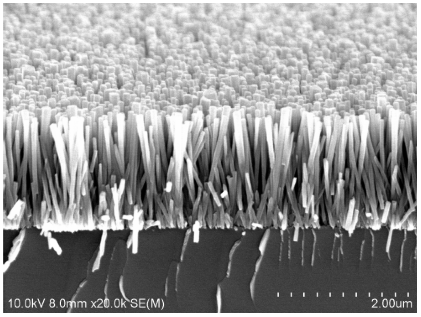
A typical SEM cross-sectional image of the as-grown nanorods is shown in Figure 1. The nanorods are distributed homogeneously and are perpendicular to the substrate with an average diameter of 80 nm and length of 1.78 . The images of the nanorods after annealing are similar to those of the as-grown ones.
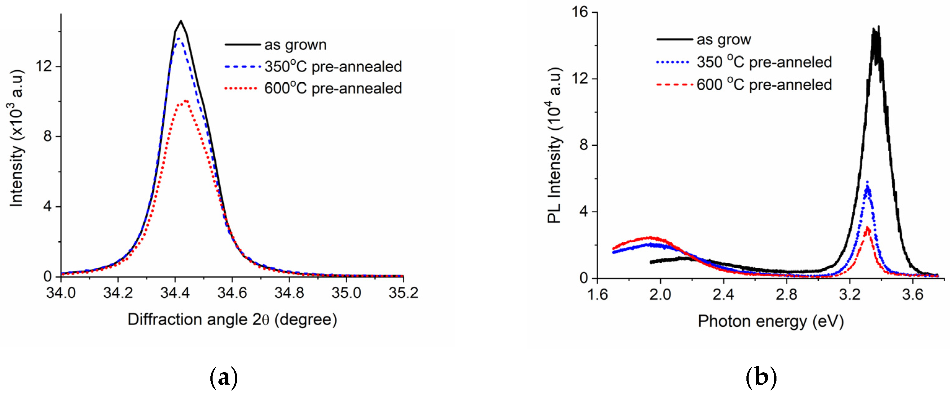
The XRD patterns of the as-grown nanorods and the annealed nanorods at different temperatures were measured. The (002) diffraction spectrum of the nanorods is shown in Figure 2a. The theoretical diffraction angle of ZnO (002) is at 34.422 degrees according to the PCPDF card (No. 36-1451), but the (002) diffraction angle of the as-grown nanorods is at 34.412 degrees, which is smaller than the theoretical value. After annealing at 350 °C, the diffraction angle shifted to a higher angle of 34.426 degrees, which is very close to the theoretical value. Meanwhile, the diffraction intensity was enhanced by a factor of 1.4 after annealing. As the annealing temperature increased to 600 °C, the diffraction angle shifted to 34.436 degrees, which is greater than the theoretical value and the diffraction intensity enhanced by a factor of 1.3 after annealing. Otherwise, the full width at half maximum (FWHM) of the diffraction peak was reduced from 0.210 degrees to 0.197 and 0.203 degrees after annealing at 350 °C and 600 °C separately. This indicated that tensile strain along the c axis existed in the as-grown nanorods. Annealing in an O2 atmosphere at 350 °C could eliminate the defects introduced by tensile stress and improve the nanorod crystal quality, but annealing at 600 °C would introduce compress strain in the nanorods. In this work, the nanorods were grown from an aqueous solution of zinc acetate and methenamine at 95 °C. There were and unreleased clusters, such as -OH, -NH, -CH, bound to Zn or O atoms in as-grown ZnO nanorods, which introduce tensile strain. Annealing the nanorods in O2 at 350 °C releases the clusters and eliminates , but annealing at 600 °C results in native defect formation and C and N atoms entering into the lattice sites, which results in compress strain.
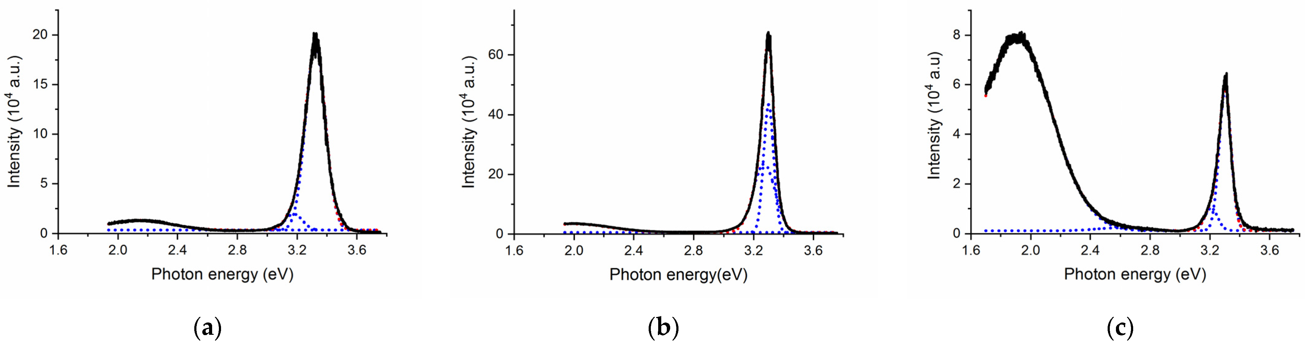
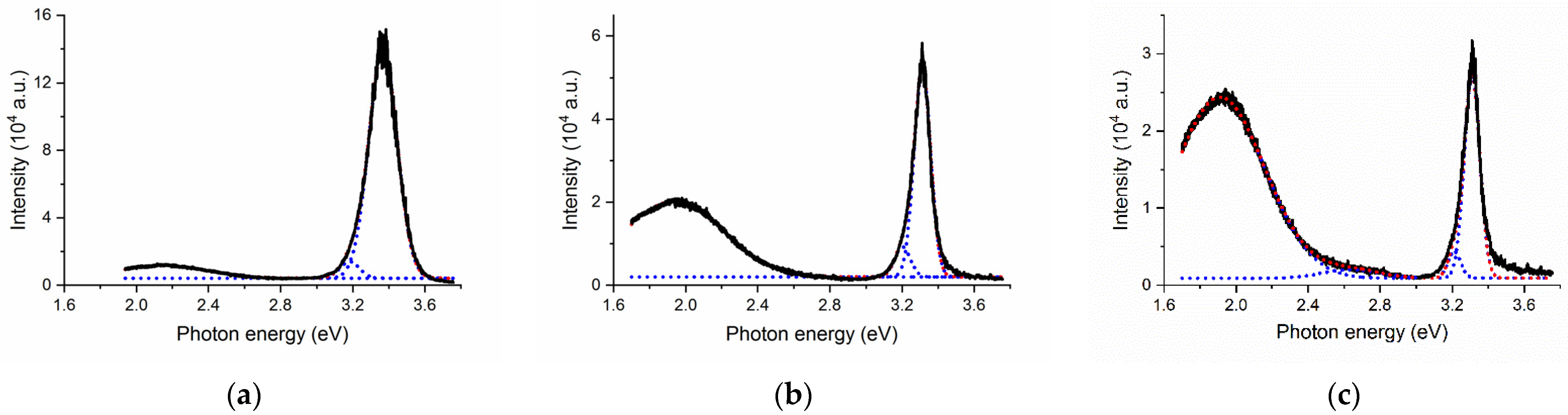
The PL spectra of the nanorods are shown in Figure 2b. A UV band from 2.90 to 3.36 eV and a visible band from 1.70 to 2.4 eV can be observed. The UV band was ascribed to exciton and near band gap shallow-defect emissions and the visible band to emissions related to deep defects [3,14]. The UV emission was enhanced dramatically after the nanorods were annealed at 350 °C, while the UV emission weakened noticeably and the deep defect-related emission was enhanced dramatically after the nanorods were annealed at 600 °C. Otherwise, the UV emission had a red shift and its FWHM narrowed after the nanorods were annealed at 350 and 600 °C. The enhancement of the UV emission in the nanorods annealed at 350 °C could be ascribed to a decrease in the non-radiation centers after annealing. The weakening of the UV emission of the nanorods annealed at 600 °C could be ascribed to the formation of non-radiation centers during annealing. To determine the emission centers, the PL spectra shown in Figure 2b were fitted with a multi-peak Gaussian function, and the results are shown in Figure 3. The emissions of the as-grown nanorods contained strong emission at 3.32 eV and weak emission at 3.18 and 2.14 eV. After the nanorods were annealed at 350 °C in an O2 atmosphere, the emission intensity at 3.30, 3.21 eV was enhanced dramatically and the emission at 2.14 eV shifted to 2.01 eV. As the annealing temperature was increased to 600 °C, the emission at 3.32 and 3.14 eV weakened. Otherwise, the emission at 2.14 eV shifted to 1.90 eV and its relative intensity enhanced dramatically after annealing at 600 °C. Very weak emission at 2.60 eV was also observed. The origin of the UV emission at 3.30–3.33 eV has been ascribed to the emission of excitons [3,18] and 3.15–3.21 eV to electron transition from the near band gap shallow defects to the valence band [12,18]. The origins of the visible emission are still under contention. Epie et al. [12] ascribed the emission around 2.10 eV to the transition from the conduction band to and the emission around 1.9 eV to transition from the conduction band to . Kaftelen et al. [20] ascribed the emission of 1.89 eV to the transition from to the valence band and the emission at 2.64 eV to the transition from the conduction band to . Dong et al. [21] ascribed the luminescence of 1.9–2.1 eV to isolated or clusters. Uklein et al. [5] determined the origins of bulk ZnO luminescence by exciting the electrons from the valence band to shallow traps or the conduction band. They attributed the emission at 2.1 and 1.8 eV to transitions from the neutral VO and/or the single-charged oxygen vacancy in the complex into the double-charged VO state. In this work, the PL spectra were measured under the excitation of a 325 nm laser, which excites the electrons from the valence band to the conduction band and forms excited excitons with energy higher than the band gap. The excited excitons quickly relaxe to the exciton ground state through interaction with phonons. Then either the excitons are annihilated directly and emit 3.3 eV of UV light, or they are captured by non-radiative centers/or radiative centers and annihilate without an emission/or with an emission of visible light. The formation energy of and is much lower than that of and in an O rich atmosphere [20]. Otherwise, isolated could be annealed out at 335 K, at 439 K, and at 219 K [22]. Annealing the nanorods in an O2 atmosphere led to the disappearance of the emission at 2.14 eV in the as-grown nanorods and an emergency emission at 2.01 eV and 1.90 eV. Then, the emission at 2.14 eV could be ascribed to the transition from the conduction band to . The emissions at 1.90, 2.01, and 2.64 eV could be ascribed to emissions from the conduction band to different states of .
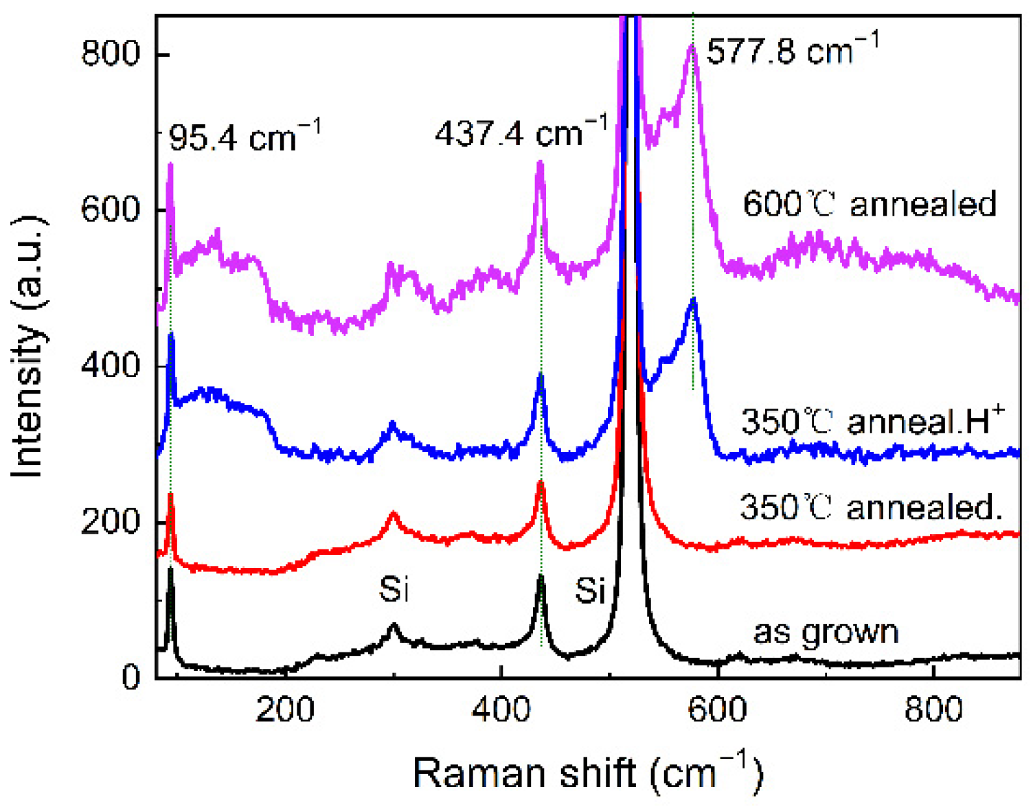
To further investigate the defect types in the nanorods, Raman spectra of the as-grown and annealed nanorods were measured and are shown in Figure 4. Raman modes at 94 cm−1 and 437 cm−1 were observed in the as-grown and annealed nanorods, but a broad peak at 577 cm−1, a weak peak at 555 cm−1, and a broad band from 97 to 200 cm−1 as a tail of 94 cm−1 vibration were observed only in the nanorods annealed at 600 °C. The 94 and 437 cm−1 modes are E2 (low) and E2 (high) vibrations of ZnO, respectively. E2 (low) had an obvious red shift compared with 98 and 101 cm−1, and E2 (high) had no shift compared with 436 cm−1, as reported in references [23,24]. E2 (high) is associated with the vibration of O sublattices. E2 (low) mode is related to the vibration of Zn sublattices. The red shift of E2 (low) in Figure 4 should be ascribed to the distortion of the Zn sublattice. 575 cm−1 is associated with the deformation or disorder induced by the defects in ZnO [18], but the origins of the tailing of E2 low Raman mode and 575 cm−1 are still controversial. Mondal et al. [25] ascribed the tailing of E2 low Raman mode and 555 cm−1 to the deformation of the Zn sublattices due to the presence of nonradiative defects and ascribed the broad vibration around 575 cm−1 to A1(LO). Song et al. [26] ascribed the tailing of E2 low Raman mode to Zn interstitials and the vibration absorption peak of 526–600 cm−1 to . Guo et al. [27] observed the broad mode around 575 cm−1 in Al, Sb, Mn doped ZnO and declared that A1(LO) mode should not be ascribed to . In this work, the tailing of E2 low Raman mode, weak vibration at 555 cm−1, and the strong vibration at 575 cm−1 were observed in the nanorods annealed at 600 °C in an O2 atmosphere rather than in the as-grown nanorods and in the nanorods annealed at 350 °C. The density of the nonradiative center and was much higher in the nanorods annealed at 600 °C, as indicated in Figure 2b. Then, the tailing of E2 low Raman mode in Figure 4 could be ascribed to the nonradiative center. The broad vibration around 575 cm−1 could ascribed to A1(LO) mode, due to the presence of impurity defects such as C and H atoms. From the discussion above, it can be seen that the defects found were different in the as-grown nanorods and the nanorods annealed at different temperatures.
3.2. Radiation Resistance of ZnO Nanorods
The XRD spectra of the nanorods after irradiation are shown in Figure 5a. The diffraction angle of the as-gown nanorods shifted to 34.420 degrees, which is close to the theory value, and its FWHM decreased to 0.186 degrees. Otherwise, the diffraction intensity enhances to 1.6 times the amount before irradiation. Obviously, H+ ion irradiation improves the as-grown nanorod crystal quality and releases the tensile stress in the nanorods. This can be attributed to the strong, dynamic annealing of the nanorods during H+ ion implanting [10]. This will be discussed in detail in combination with ion energy loss. The diffraction intensity of the nanorods pre-annealed at 350 °C was similar to that before irradiation (Figure 2a), but the diffraction angle shifted slightly towards a lower angle of 42.418 degrees after irradiation. H+ ion irradiation had some slight effects on the crystal quality of the nanorods pre-annealed at 350 °C, but it induced a degree of slight tensile stress in them. As for the nanorods pre-annealed at 600 °C, the diffraction intensity decreased to 89% of the amount before irradiation. Meanwhile, the diffraction angle shifted to a lower angle of 34.429 degrees, which is close to the theory value. Clearly, H+ ion irradiation degraded the crystal quality of the nanorods pre-annealed at 600 °C and partially released the compress strain in the nanorods. Comparing the crystal quality of the nanorods before and after annealing, and before and after irradiation, it could be seen that the crystal quality of the as-grown nanorods after irradiation was superior to that of the nanorods annealed at 350 °C before irradiation, which was superior to that of the nanorods annealed at 600 °C before irradiation. It is evident that H+ irradiation effects are very sensitive to the nanorod initial states. Defects in the nanorods before irradiation have remarkable effects on radiation resistance. The appropriate and -CH and -NH impurities could help the nanorods improve their crystal quality, but the high density of in the nanorods would degrade the nanorod crystal quality under H+ ion irradiation.
To investigate H+ ion irradiation effects on the nanorod optical properties, Figure 5b shows PL spectra of the nanorods after irradiation. The emissions of all H+ ion irradiated nanorods weakened. However, the variation of the PL spectra after irradiation was different for the nanorods with different initial states. The peak intensity of UV emission decreased to 78% of the value before irradiation for the as-grown nanorods. The visible light was almost unchanged and the ratio of visible-to-UV emission increased from 0.07 to 0.08. H+ ion irradiation introduced non-radiative centers, which weakened the UV emission in the as-grown nanorods. The peak intensity of the UV emission reduced to 8%, while the visible emission reduced to 56% of the amount before irradiation for the nanorods pre-annealed at 350 °C. The ratio of the visible-to-UV light increased from 0.05 to 0.35 after irradiation. Furthermore, the UV emission of the nanorods pre-annealed at 350 °C was weaker than that of the as-grown nanorods after irradiation. Clearly, H+ ion irradiation degraded the emission of the nanorods pre-annealed at 350 °C dramatically. The effects of H+ ion irradiation on the nanorods pre-annealed at 600 °C were quite different from those of the as-grown nanorods and the nanorods pre-annealed at 350 °C. The UV emission peak intensity reduced to 49% of that before irradiation, but the ratio of the visible-to-UV light reduced from 1.23 to 0.74 after irradiation. H+ ion irradiation weakened the visible light emission more efficiently than the UV emission in nanorods pre-annealed at 600 °C. After H+ ion irradiation, the emission intensity of the as-grown nanorods was superior to that of the nanorods pre-annealed at 350 °C, which was superior to that of the nanorods pre-annealed at 600 °C. The variation in the emission of nanorods before and after H+ ion irradiation was consistent with the change in the nanorod crystal quality. The as-grown nanorods showed better crystal and optical stability than the nanorods pre-annealed in an O2 atmosphere under H+ ion irradiation. This means that the difference in defect types and the concentration before irradiation affects the evolution of the defects during H+ ion irradiation.
To further investigate the effects of H+ ion radiation on the variation in defect types, the PL spectra of the nanorods after irradiation were fitted by Gaussian function and are shown in Figure 6. A strong emission at 3.36 eV and a weak emission at 3.18 eV and 2.14 eV were observed in the as-grown nanorods after irradiation. When comparing with the PL spectra before irradiation in Figure 3a, the UV emission had a blue shift from 3.32 to 3.36 eV. No other new emission centers were observed. In the nanorods pre-annealed at 350 °C, a strong emission at 3.30 eV and a weak emission at 3.21 and 1.90 eV were observed after irradiation. The visible emission shifted from 2.01 eV to 1.90 eV after irradiation. In addition, 1.9 eV emission was observed in the nanorods annealed at 600 °C before irradiation. This means that irradiation changes the type of the emission centers in the nanorods pre-annealed at 350 °C and that the type of irradiation-induced defect found is similar to that introduced by annealing the nanorods in the O2 at 600 °C. In the nanorods annealed at 600 °C, a strong emission at 3.30 and 1.90 eV and a very weak emission at 3.21 and 2.60 eV similar to that before irradiation were observed. Irradiation does not introduce new emission centers but changes the concentration of the emission centers. To further identify the similarity of the defects introduced by H+ ions in the nanorods pre-annealed at 350 °C with those introduced by annealing at 600 °C in an O2 atmosphere, A Raman spectrum of the nanorods pre-annealed at 350 °C after irradiation is also shown in Figure 4. The tailing of E2 low Raman mode, a broad peak at 577 cm−1, and a weak peak at 555 cm−1 were also observed, which was the same as those observed in the nanorods annealed at 600 °C before irradiation. This confirms that the defect type introduced by H+ ions in the nanorods pre-annealed at 350 °C is similar to that in the nanorods introduced by annealing at 600 °C in an O2 atmosphere.
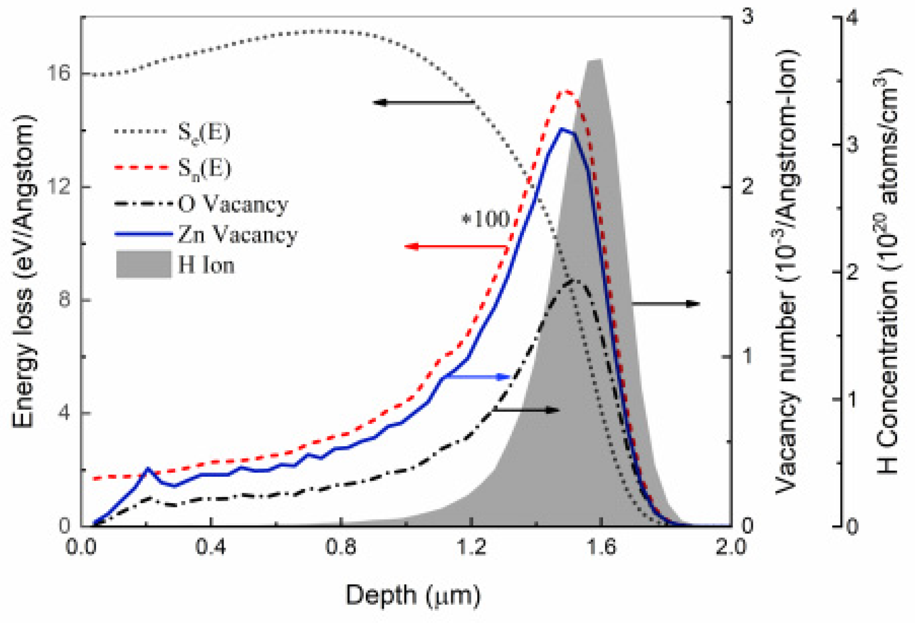
Energetic H+ ions lose their energy by electronic energy loss (Se) and nuclear energy loss (Sn) in materials. The depth distribution of the Se and Sn of H+ ions and the concentrations of and introduced by 180 keV H+ ions calculated with SRIM-TRIM (2013) are shown in Figure 7. The distribution of the stopped H atoms is also shown. It can be seen that Se was much higher than Sn before H+ resting in the nanorods. H+ ions lost their energy mainly by Se. H+ ions displaced the Zn and O lattice atoms directly by Sn and resulted in the formation of vacancies and interstitials. concentration was much higher than that of the after 180 keV H+ ion irradiation, as shown in Figure 7. This means much more and than and were introduced in the nanorods by H+ ions. H+ ions were also able to excite electrons to high energy levels [12] and excite phonons by Se. The vibration of lattices could result in the rising of the nanorod temperature. Interstitials in the nanorods are more movable than the vacancies [22]. Heat produced by the Se of H+ ions enabled the interstitials produced by irradiation at an early stage to move to the surfaces of the nanorods and the immovable and would remain in the nanorods which could capture the newly produced interstitials. Then, the irradiation defects were able to be annihilated in a degree. The (002) diffraction angle and the intensity of the as-grown nanorods after irradiation (Figure 5) were very close to those for the nanorods annealed at 350 °C before irradiation (Figure 2). It could be deduced that the thermal effect of H+ ion irradiation for the as-grown nanorods is equivalent to the annealing effect around 350 °C in an O2 atmosphere. This temperature could enable interstitials to move to the nanorod surfaces and enable the release of the superfluous -CH and -NH clusters bounded to the Zn and O atoms but be too low to enable the formation of native defects. Then, the crystal quality could be improved by thermal effects and the strain in the nanorods could be released after irradiation. In the nanorods pre-annealed at 350 °C, the native defect density was much lower than that in the as-grown nanorods. In the initial state of irradiation, and introduced by the Sn could either be annealed or diffuse to the nanorod surfaces due to the thermal effects of irradiation. Then, the remaining vacancies captured the newly produced and and the nanorod crystal quality was stable under irradiation, but the thermal effects of H+ ions could not anneal the irradiation-induced non-radiation centers, and the nanorod emission degraded dramatically. In the nanorods annealed at 600 °C, the and non-radiation centers of had been introduced before irradiation. During H+ ion irradiation, the displaced atoms produced by irradiation and the rested H+ ions were able to be trapped or stabilized by the and and form stable defects and their clusters. Then, the crystal quality of the nanorods was degraded after irradiation. Otherwise, annealing introduced before irradiation was able to capture the introduced by H+ ions. Then the concentration of clusters decreased and the relative intensity of UV to visible emission increased.
4. Conclusions
The crystal and optical properties of the ZnO nanorods after H+ ion irradiation depend upon the pre-existed defects in the nanorods. Irradiation could improve the crystal quality of the as-grown nanorods with , while it degrades the crystal quality of the nanorods pre-annealed at 600 °C with a high density of . The crystal quality of the nanorods annealed at 350 °C with fewer defects is stable under irradiation. The thermal effects of irradiation play an important role in the property variation of nanorods under irradiation, and the effective temperature for irradiation is around 350 °C. The optical properties of the as-grown nanorods are quite stable under irradiation compared with those of the annealed ones. Irradiation introduces nonradiative centers which are also responsible for the tailing of E2 low Raman mode. Irradiation also increases concentration in the nanorods pre-annealed at 350 °C and decreases the relative concentration of in the nanorods pre-annealed at 600 °C. The degradation of the emission by ion irradiation is quite obvious in the nanorods annealed at 350 °C with fewer pre-existed defects. The visible centers introduced by the H+ ions in the nanorods pre-annealed at 350 °C are similar to those in the nanorods introduced by annealing at 600 °C in an O2 atmosphere.
Author Contributions
T.W., sample growth, SEM, and writing; A.W., XRD Experiments; M.W., PL spectrum and data process; Y.W., design, supervision, and review; Z.L. and Y.H., data process; Z.W., PL spectrum; G.W., H+ irradiation. All authors have read and agreed to the published version of the manuscript.
Funding
This research was funded by Beijing NOVA Program (Z181100006218121).
Data Availability Statement
Not applicable.
Acknowledgments
The authors thank Zheng Li (College of Nuclear Science and Technology, Beijing Normal University) for his help of ion implantation experiments.
Conflicts of Interest
The authors declare no conflict of interest.
References
- Özgür, Ü.; Alivov, Y.I.; Liu, C.; Teke, A.; Reshchikov, M.; Doğan, S.; Avrutin, V.C.S.J.; Cho, S.J.; Morkoç, H. A comprehensive review of ZnO materials and devices. J. Appl. Phys. 2005, 98, 11. [Google Scholar] [CrossRef] [Green Version]
- Consonni, V.; Lord, A.M. Polarity in ZnO nanowires: A critical issue for piezotronic and piezoelectric devices. Nano Energy 2016, 8, 7631. [Google Scholar] [CrossRef]
- Tang, K.; Gu, S.L.; Ye, J.D.; Zhu, S.M.; Zhang, R.; Zheng, Y.D. Recent progress of the native defects and p-type doping of zinc oxide. Chin. Phys. B 2017, 26, 047702. [Google Scholar] [CrossRef]
- Shahzad, S.; Javed, S.; Usman, M. A Review on Synthesis and Optoelectronic Applications of Nanostructured ZnO. Front. Mater. 2021, 8, 613825. [Google Scholar] [CrossRef]
- AUklein, V.; Multian, V.V.; Kuz’micheva, G.M.; Linnik, R.P.; Lisnyak, V.V.; Popov, A.I.; Ya, G.V. Nonlinear optical response of bulk ZnO crystals with different content of intrinsic defects. Opt. Mater. 2018, 84, 738–747. [Google Scholar] [CrossRef]
- Khaliullin, S.M.; Zhuravlev, V.D.; Ermakova, L.V.; Buldakova, L.Y.; Yanchenko, M.Y.; Porotnikova, N.M. Solution Combustion Synthesis of ZnO Using Binary Fuel (Glycine + Citric Acid). Int. J. Self-Propagating High-Temp. Synth. 2019, 28, 226–232. [Google Scholar] [CrossRef]
- Sathishkumar, P.; Li, Z.F.; Raji, G. Zinc oxide-quercetin nanocomposite as a smart nano-drug delivery system: Molecular-level interaction studies. Appl. Surf. Sci. 2021, 536, 147741. [Google Scholar] [CrossRef]
- Li, W.Q.; Zhan, X.Y.; Song, X.Y.; Si, S.Y.; Chen, R.; Liu, J.; Wang, Z.X.; He, J.; Xiao, X.H. A review of recent applications of ion beam techniques on nanomaterial surface modification. Nano Energy 2019, 15, 1901820. [Google Scholar]
- Nakayama, R.; Maesato, M.; Lim, G.C.; Arita, M.; Kitagawa, H. Heavy hydrogen doping into ZnO and the H/D isotope effect. J. Am. Chem. Soc. 2021, 143, 6616–6621. [Google Scholar] [CrossRef]
- Das, A.; Basak, D. Efficacy of ion implantation in zinc oxide for optoelectronic applications A Review. ACS Appl. Electron. Mater. 2021, 3, 3693–3714. [Google Scholar] [CrossRef]
- Chan, K.S.; Vines, L.; Johansen, K.M.; Monakhov, E.V.; Ye, J.D.; Parkinson, P.; Jagadish, C.; Svensson, B.G.; Wong-Leung, J. Defect formation and thermal stability of H in high dose H implanted ZnO. J. Appl. Phys. 2013, 114, 083111. [Google Scholar] [CrossRef]
- Epie, E.N.; Chu, W.K. Ionoluminescence study of Zn− and O− implanted ZnO crystals: An additional perspective. Appl. Surf. Sci. 2016, 371, 28–34. [Google Scholar] [CrossRef]
- Neuvonen, P.T.; Vines, L.; Svensson, B.G.; Kuznetso, A.Y. Intrinsic point-defect balance in self-ion-implanted ZnO. Phys. Rev. Lett. 2013, 110, 015501. [Google Scholar] [CrossRef] [PubMed] [Green Version]
- Wu, T.F.; Wang, A.J.; Zheng, L.; Wang, G.F.; Tu, Q.Y.; Lv, B.; Liu, Z.L.; Wu, Z.L.; Wang, Y.S. Evolution of native defects in ZnO nanorods irradiated with hydrogen ion. Sci. Rep. 2019, 9, 17393. [Google Scholar] [CrossRef]
- Look, D.C.; Reynolds, D.C.; Hemsky, J.W.; Jones, R.L.; Sizelove, J.R. Production and annealing of electron irradiation damage in ZnO. Appl. Phys. Lett. 1999, 75, 811. [Google Scholar] [CrossRef] [Green Version]
- Lorenza, K.; Alves, E.; Wendler, E.; Bilani, O.; Hayes, W.W. Damage formation and annealing at low temperatures in ion implanted ZnO. Appl. Phys. Lett. 2015, 87, 191904. [Google Scholar] [CrossRef]
- Rehman, N.U.; Mehmood, M.; Ali, S.M.; Ramay, S.M.; Shar, M.A.; Algarawi, M.S. Annealing induced defects in ZnO nanostructures. Appl. Phys. A 2019, 125, 528. [Google Scholar] [CrossRef]
- Ruane, W.T.; Johansen, K.M.; Leedy, K.D.; Look, D.C.; Wenckstern, H.V.; Grundmann, M.; Farlow, G.C.; Brillson, L.J. Defect segregation and optical emission in ZnO nano- and microwires. Nanoscale 2016, 8, 7631. [Google Scholar] [CrossRef] [Green Version]
- Azarov, A.; Wendler, E.; Lorenz, K.; Monakhov, E.; Svensson, B.G. Effect of buried extended defects on the radiation tolerance of ZnO. Appl. Phys. Lett. 2017, 110, 172103. [Google Scholar] [CrossRef]
- Kaftelen, A.H.; Ocakoglu, K.; Thomann, R.; Tu, S.Y.; Weber, S.; Erdem, E. EPR and photoluminescence spectroscopy studies on the defect structure of ZnO nanocrystals. Phys. Rev. B 2012, 86, 014113. [Google Scholar] [CrossRef]
- Dong, Y.F.; Tuomisto, F.; Svensson, B.G.; Kuznetsov, A.Y.; Brillson, L.J. Vacancy defect and defect cluster energetics in ion-implanted ZnO. Phys. Rev. B 2010, 81, 081201. [Google Scholar] [CrossRef] [Green Version]
- Janotti, A.; van de Walle, C.G. Native point defects in ZnO. Phys. Rev. 2007, B76, 165202. [Google Scholar] [CrossRef]
- Cuscó, R.; Alarcón-Lladó, E.; Ibáñez, J.; Artús, L.; Jiménez, J.; Wang, B.; Callahan, M.J. Temperature dependence of Raman scattering in ZnO. Phys. Rev. B 2007, 75, 165202. [Google Scholar] [CrossRef]
- Silva, R.L.D.E.; Franco, A. Raman spectroscopy study of structural disorder degree of ZnO ceramics. Mater. Sci. Semicon. Proc. 2020, 119, 105227. [Google Scholar] [CrossRef]
- Mondal, A.; Pal, S.; Sarkar, A.; Bhattacharya, T.S.; Pal, S.; Singha, A.; Ray, S.K.; Kumar, P.; Kanjilal, D.; Jana, D. Raman investigation of N-implanted ZnO: Defects, disorder and recovery. J. Raman Spectrosc. 2019, 50, 1926–1937. [Google Scholar] [CrossRef]
- Song, Y.; Gou, J.; Yang, Y.T.; Ding, Z.N.; Zhang, S.X.; Zhang, C.H. Microstructure property study of ZnO single crystal irradiated with 200 MeV 86Kr17+ ions. Mater. Res. Express 2019, 6, 026203. [Google Scholar]
- Guo, S.; Du, Z.; Dai, S. Analysis of Raman modes in Mn-doped, ZnO nanocrystals. Phys. Status Solidi B 2009, 246, 2329–2332. [Google Scholar] [CrossRef] [Green Version]
Figure 1.
The cross-sectional SEM image of the as-grown nanorods.

Figure 2.
(a) XRD spectra (b) PL spectra of ZnO nanorods before and after annealing at different temperatures.
Figure 2.
(a) XRD spectra (b) PL spectra of ZnO nanorods before and after annealing at different temperatures.

Figure 3.
Fitting of PL spectra with multi-peak Gaussian function (a) as grown nanorods and nanorods (b) annealed at 350 °C (c) annealed at 600 °C. The solid lines are the experimental results. The dotted blue lines represent the Gaussian fitting of the different transition emission and the red line their sum.

Figure 4.
Raman spectra of ZnO nanorods.

Figure 5.
(a) XRD spectra (b) PL spectra of ZnO nanorods after they are irradiated with H+ ions.

Figure 6.
Fitting of the PL spectra with multi-peak Gaussian function (a) as-grown nanorods and nanorods annealed at (b) 350 °C (c) 600 °C after H+ ion irradiation. The solid lines are the experimental results. The dotted blue lines represent the Gaussian fitting of the different transition emission and the red line their sum.

Figure 7.
The depth distribution of Se and Sn of H+ ions, and and introduced by 180 keV H+ ions and rested H+ ions calculated with SRIM-TRIM (2013).
Figure 7.
The depth distribution of Se and Sn of H+ ions, and and introduced by 180 keV H+ ions and rested H+ ions calculated with SRIM-TRIM (2013).

Publisher’s Note: MDPI stays neutral with regard to jurisdictional claims in published maps and institutional affiliations. |
© 2022 by the authors. Licensee MDPI, Basel, Switzerland. This article is an open access article distributed under the terms and conditions of the Creative Commons Attribution (CC BY) license (https://creativecommons.org/licenses/by/4.0/).
Share and Cite
MDPI and ACS Style
Wu, T.; Wang, A.; Wang, M.; Wang, Y.; Liu, Z.; Hu, Y.; Wu, Z.; Wang, G. Effects of Pre-Annealing on the Radiation Resistance of ZnO Nanorods. Crystals 2022, 12, 1007. https://0-doi-org.brum.beds.ac.uk/10.3390/cryst12071007
AMA Style
Wu T, Wang A, Wang M, Wang Y, Liu Z, Hu Y, Wu Z, Wang G. Effects of Pre-Annealing on the Radiation Resistance of ZnO Nanorods. Crystals. 2022; 12(7):1007. https://0-doi-org.brum.beds.ac.uk/10.3390/cryst12071007
Chicago/Turabian StyleWu, Tengfei, Aiji Wang, Mingyu Wang, Yinshu Wang, Zilin Liu, Yiwen Hu, Zhenglong Wu, and Guangfu Wang. 2022. "Effects of Pre-Annealing on the Radiation Resistance of ZnO Nanorods" Crystals 12, no. 7: 1007. https://0-doi-org.brum.beds.ac.uk/10.3390/cryst12071007
Note that from the first issue of 2016, this journal uses article numbers instead of page numbers. See further details here.