Article

Pyroelectric and Ferroelectric Properties of Hafnium Oxide Doped with Si via Plasma Enhanced ALD

by
Markus Neuber
,
Maximilian Walter Lederer
*,†,
Konstantin Mertens
,
Thomas Kämpfe
,
Malte Czernohorsky
and
Konrad Seidel
Fraunhofer IPMS CNT, 01109 Dresden, Germany
*
Author to whom correspondence should be addressed.
These authors contributed equally to this work.
Submission received: 18 July 2022 / Revised: 3 August 2022 / Accepted: 4 August 2022 / Published: 9 August 2022
(This article belongs to the Special Issue Research and Development of Ferroelectric Material)

Abstract

:
Devices based on ferroelectric hafnium oxide are of major interest for sensor and memory applications. In particular, Si-doped hafnium oxide layers are investigated for the application in the front-end-of-line due to their resilience to high thermal treatments. Due to its very confined doping concentration range, Si:HfO2 layers based on thermal atomic layer deposition often exhibited a crossflow pattern across 300 mm wafer. Here, plasma enhanced atomic layer deposition is explored as an alternative method for producing Si-doped HfO2 layers, and their ferroelectric and pyroelectric properties are compared.

1. Introduction

With the discovery of ferroelectricity in hafnium oxide thin films [1], which has been previously employed as high-k dielectric in high-k-metal-gate (HKMG) complementary-metal-oxide-semiconductor (CMOS) processes, researchers showed strong interest for the integration of this material into novel devices. Applications range from non-volatile memories [2,3] and neuromorphic devices [4,5] to piezoelectric micro-electro-mechanical-systems (MEMS) [6,7,8], energy harvesting devices [9] and pyroelectric sensors [10,11]. The great interest in this material stems not only from its CMOS compatibility but also red from its unique properties: a high coercive field, combined with high remanent polarization and comparably low relative permittivity [12].
Nevertheless, due to its metastable nature, the ferroelectric phase in hafnium oxide has to be stabilized by means using reduced thicknesses, mechanical stress or dopants [13,14,15]. Since most films are of polycrystalline nature, layers often include polymorphs, especially the monoclinic phase, which resembles the thermodynamical ground state [16,17]. Consequently, controlling the phase composition of the thin film is crucial for the application, e.g., for the device-to-device variation in ferroelectric memories [18,19,20]. Recent investigations have highlighted how the microstructure and phase composition can be influenced by different doping elements, concentrations, substrate and annealing temperature [21,22,23,24,25,26]. Moreover, a close link between the ferroelectric response and the formation of 90° domains in conjunction with the presence of crystallographic textures has been drawn [27]. An often overlooked factor, however, has been the dopant distribution inside the layer, as well as differences in their deposition. Nevertheless, recent results indicate that the heterostructure of HfxZr1-xO2, more precisely the number of cycles before alternating between the two elements (Hf, Zr), influences the microstructure of the thin film [28].
In this study, the influence of the deposition process of the Si-doping is explored by comparing thermal- and plasma-enhanced atomic layer deposition. This does not only impact the variability across 300 mm wafers but also provides insight into the influence of the dopant layer on the pyroelectric and ferroelectric behavior of Si-doped hafnium oxide (HSO).

2. Materials and Methods

In order to understand the differences in the deposition process of the Si-dopant, the sample preparation and (plasma enhanced) atomic-layer deposition (ALD) are explained. Afterwards, details on the different measurement methods are provided.

2.1. Atomic Layer Deposition of HSO

The silicon doped hafnium oxide layer in this study is deposited using a series combination of processes in an ASM Pulsar3000 and an EmerALD chamber. The hafnium oxide was deposited by thermal atomic layer deposition with hafnium(IV)-chloride (HfCl4) and water at 300 °C in the Pulsar chamber. Silicon oxide, on the other hand, was either thermally grown via ALD in the Pulsar3000 chamber using SiCl4 and water or formed in the EmerALD chamber by cycling bis(diethylamino)silane, also known as SAM24, and oxygen at 50 °C. The latter process is supported by a capacitively coupled argon plasma, thus resembling a plasma-enhanced (PE) ALD deposition process. The doping concentration of silicon is set by the amount and frequency of SiO2 (PE)ALD cycles between the HfO2 cycles. In this study, one cycle of SiO2 is run after 16, 26 and 32 cycles of HfO2 in the case of the PEALD Si-doping process, respectively. The resulting HSO layers are denoted as hybrid HSO. This process was compared with our standard HSO process, which is entirely run via thermal ALD with cycling ratios of 10:1, 14:1, 16:1, 20:1 and 27:1. In both cases, the total film thickness was 10 nm.
Titanium nitride films of 10 nm thickness were used for the bottom and top electrodes and were deposited via ALD and physical vapour deposition (PVD), respectively. Three hundred millimeter highly doped bare Si wafers were used as substrate. After the formation of the material stack, the resulting films of silicon-doped hafnium oxide were thermally treated at 800 °C for 20 s in a nitrogen atmosphere. This is necessary to form a polar ferroelectric crystal structure. For the electrical characterization, metal dots (Ti/Pt) were deposited and separated with a wet-etch process.

2.2. Metrology

The thickness of all thin films was measured via spectral ellipsometry on a Spectra FX100. The mean thickness was calculated out of 49 points and arranged radially with an edge exclusion of 3 mm. X-ray photoelectron spectroscopy (XPS) on a ReVera Veraflex with an Al K α source was used to determine the stoichiometry of these films. After the thermal treatment, grazing incident X-ray diffraction (GIXRD) was employed to investigate the presence and proportion of crystallographic phases in the HSO. XRD was performed on Bruker Discover D8 at a grazing angle of 0.5°.
The ferroelectric polarization measurements were executed on a Suess PA300 semiautomatic shielded probe station using an Aixacct TF3000 analyzer with a triangular waveform at a frequency of 1 kHz and at an amplitude of 3 V.
The pyroelectric properties, on the other hand, were determined on a LA100 station of Semiprobe with a Keysight B2981 picoammeter. The determination of the pyroelectric coefficient was executed following the Garn–Sharp-method [10,29].

3. Results

In order to gain insight into the influence of the Si-doping deposition process, structural, chemical and electrical analyses were performed. The results of these measurements are presented below.

3.1. Structural and Chemical Analysis

The ratio of silicon and hafnium oxide ALD cycles was adjusted so that all processes yield roughly the same thickness of 10 nm. The result is presented in Table 1. While films deposited with the standard ALD process exhibit thicknesses of 10.6 to 11.1 nm, the ones that had a SiO2 deposited with PEALD are thicker and were found between 11.8 and 12.7 nm. The standard deviation of the film thickness was roughly the same for both processes (between 3.2 and 3.7%). The differences in the pattern of the HSO thickness can be explained by the design of the ALD chambers. While the thermal reactor was built with a crossflow design, where the precursors and the byproducts flow across the entire wafer, the plasma ALD reactor has a show head, letting the gas flow from the center to the edge of the wafer.
Figure 1 illustrates the wafer map of both process types with a 16:1 ratio. The standard HSO process (Figure 1a) demonstrates a linear decrease in the film’s thickness from the gas inlet to the gas outlet. The film deposited with the hybrid process (Figure 1b) shows a ring-like pattern, with the higher thickness at the edge of the wafer instead of at the wafer’s center where the gas inlet is located. The global maximum of the film thickness is located at the gas outlet. The reason for this effect is diverse, e.g., the gradient of chuck temperature, plasma power, the flow of gases and their byproducts.
The results of the XPS displayed in Table 1 also indicate a higher Si content in the films deposited with the hybrid process. Further investigations into the deposition rate of both processes have revealed a significantly higher deposition rate for PEALD compared to the thermal ALD of SiO2.
The silicon concentration in the doped hafnium oxide contributes significantly to the formation of polar crystallographic phases and, thus, the ferroelectric behavior of the material. As shown in Figure 2, the films with the lowest concentration of Si (32:1, 2.1% Si) exhibit strong signals at the diffraction lines of the orthorhombic phase. Earlier studies have shown a sweet spot of ferroelectric behaviors in HSO at 3.5% [15]. Samples with higher Si concentration show patterns fitting to orthorhomibic and tetragonal phases as well. Major differences are the reduction/absence of signals of the low angle (<25°) diffraction lines of the orthorhombic phase compared to the 32:1 sample. While those lines can also be the result of monoclinic phase presence, high concentrations of this phase in the 32:1 sample are not expected due to the absence of significant signal intensities in the most intense lines at approximately 28° and 32°.

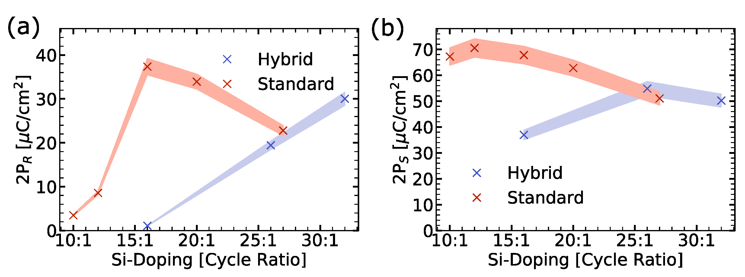
3.2. Ferroelectric Properties

In order to characterize the ferroelectric behavior of the samples, dynamic hysteresis measurements (DHMs) were conducted. The recorded polarization-voltage hysteresis for the hybrid HSO samples is shown in Figure 3a. Strong antiferroelectric-like behavior is observed for the 16:1 and 26:1 cycling ratio initially. The sample with 32:1 cycling ratio, on the other hand, shows rather ferroelectric behavior but exhibits a pronounced imprint. However, the positive imprint is not observed for the full hysteresis as a small part of the total polarization switches with a negative imprint. As a result, minor pinching is observed in the lower half of the hysteresis. Such behaviors might originate from domain pinning, as certain polarization orientations are favored. This is pinning could, e.g., be supported by the presence of oxygen vacancies.
After 10,000 electric field cycles (applied amplitude equals 3V) at 1 kHz, the hystereses of the hybrid HSO samples with 2.7% and 2.1% Si/(Hf + Si) concentration become more square-like. While the Si-rich sample of the two has transitioned to a rather ferroelectric-like behavior, the imprint of the other sample has been reduced, resulting in a centered hysteresis. The transition observed here from an antiferroelectric-like behavior to ferroelectric behavior is well known as the classical wake-up effect [27]. The physical origin of this effect has been discussed extensively in the past, and recent findings strongly support 90° domain wall movements combined with stress relaxation processes as the underlying mechanism [27,30]. An extensive discussion on this topic can be found elsewhere [27]. The reduction in imprint, on the other hand, is most likely related to defect redistribution and domain wall depinning. However, this process might be in a superposition with aforementioned wake-up effects.
In the case of the hybrid HSO sample with a 16:1 cycling ratio, stable antiferroelectric-like behavior is observed. Even after extensive electric field cycling, no significant change in behavior was detected.
Comparing the hybrid HSO with the standard HSO samples, as depicted in Figure 4, major differences are observable. (Polarization hystereses of the standard HSO samples can be found elsewhere [15].) After cycling, remanent polarization (PR) shows a clear optimum in the case of the standard HSO process (Figure 4a). For hybrid HSO, a continuous increase towards lower Si-concentrations is observed, with the highest 2PR of 30.0 μ C/cm2 in the case of the 32:1 cycling ratio. This value is a bit lower than the optimum of the standard HSO, which reaches 2PR = 37.3 μ C/cm2.
The saturated polarization (PS) after cycling (see Figure 4b) shows similar values for the cycling ratio 26:1 and 27:1 in the case of hybrid and standard HSO, respectively. Moreover, the 32:1 hybrid HSO sample continues the trend of PS, which is expected based on the standard HSO samples. The much lower PS in the case of the 16:1 hybrid HSO sample is a result of the stong antiferroelectric-like behavior, resulting in not fully switched polarizations and, consequently, reduced PS.

3.3. Pyroelectric Properties

As described in Section 2.2, the Garn–Sharp method was used to determine the pyroelectric coefficient of the HSO thin films. The applied temperature was oscillating with a sinusoidal with a Δ T of 5 K. This temperature function was applied using a Peltier element connected to a Keysight B2901 source multimeter. A Pt100 sensor was connected to the sample to control the temperature. The resulting pyroelectric current has a low signal current in the range of pA and was, therefore, measured with a Keysight B2981 electrometer.
The pyroelectric coefficient was calculated with the equation below [10]:
p = I RMS s i n ( ϕ ) A 2 π f T RMS ,
with the total area A of the ferroelectric film, the frequency of the measurement is denoted by f, the phase shift ϕ between set temperature and measured pyroelectric current I RMS and the root mean square (RMS) values of temperature TRMS.
Figure 5a shows a phase shift of 93°. This small mismatch of 3% can be attributed to a flawed thermal connection between either the sample and the Peltier element or the sample and the temperature sensor. The IRMS of this measurement is about 1 pA. Figure 5b compares the pyroelectric coefficient of the standard and hybrid HSO over the Si-doping concentration in the film. The standard HSO peaked around 116 μ C/m 2 K while the hybrid HSO only reached 83 μ C/m 2 K. Further studies with more Si concentrations within this range have to be conducted to observe whether the true peak of the pyroelectric coefficient was found for the hybrid HSO.

4. Discussion

Due to the different deposition chambers and approaches, the hybrid HSO layers show no crossflow patterns and offer a more precise doping control. This is not only reflected on the one side in lower deviations in doping content but also on the other side in the much lower deviation in the quantity of the pyroelectric coefficient.
A major drawback, however, is the slightly thicker SiO2 ALD-monolayer in the PEALD process (as illustrated in Figure 6a). As a result, the Si-doping concentration clearly shifted to higher values when compared to the thermal ALD counterpart (see Figure 6b and Table 1). In the remanent polarization results (Figure 4a), a clear shift is observable and strong antiferroelectric-like contributions have been identified in the polarization hystereses (Figure 3). It is nicely observable that this is a result of the difference in Si-doping concentrations when comparing the remanent polarization against Si-concentration, as shown in Figure 6c. The observed trend nicely fits with the trend observed for standard HSO.
Nevertheless, further differences remain. PS values are smaller than the standard HSO flow and fit better to the observed trend for the thermal ALD-deposited samples when plotting versus the cycling ratio (ignoring the outlier due to strong antiferroelectric-like behavior). Furthermore, the pyroelectric coefficient still show a remaining shift towards higher concentrations when normalized against Si concentrations compared to the standard HSO samples. A possible explanation for the observed differences is, therefore, the difference in the thickness of the SiO2 ALD-monolayer. As mentioned, other groups have reported a strong influence of the doping-layer thickness on the microstructure when investigating hafnium zirconium oxide [28]. A change in the microstructure would also explain differences observed here. Differences in PS values for predominantly orthorhombic hafnium oxide films often originate from changes in crystallographic texture [27]. Moreover, the peak in the pyroelectric coefficient has been related to the boundary where a transition between antiferroelectric-like and ferroelectric behavior takes place [31]. Since this transition is strongly influenced by the residual stress inside the layer [15,27], a change in microstructure will shift the location of the aforementioned boundary. Consequently, the here presented results highlight the importance of the dopant’s position and distribution prior to the crystallization’s annealing process, both on the structural as well as electrical properties of the resulting pyro-/ferroelectric thin film.

5. Conclusions

In conclusion, the structural, chemical and ferro- and pyroelectric properties of hybrid HSO have been explored. The results clearly indicate an improved uniformity of doping using the PEALD-based approach compared to the thermal ALD-based standard HSO thin film. Due to a difference in the ALD-monolayer thickness, influences in the Si-doping concentration and distribution could be identified. It can be concluded that both the dopant concentration and the distribution thereof strongly influence the pyro- and ferroelectric properties. Consequently, the design of the dopant deposition process is expected to strongly influence the device’s performance.

Author Contributions

Conceptualization, K.M., M.W.L. and M.N.; methodology, M.N. and K.M.; validation, M.W.L., M.N. and K.S.; formal analysis, K.M. and M.N.; investigation, M.W.L.; resources, M.W.L.; data curation, M.W.L.; writing—original draft preparation, M.W.L. and M.N.; writing—review and editing, M.W.L., K.S. and T.K.; visualization, M.W.L. and M.N.; supervision, M.C., T.K. and K.S.; project administration, M.C. and T.K.; funding acquisition, M.C. and T.K. All authors have read and agreed to the published version of the manuscript.

Funding

This research was funded by the ECSEL Joint Undertaking project OCEAN12 in collaboration with the European Union’s Horizon 2020 Framework Program for Research and Innovation (H2020/2014-2020) and National Authorities, under Grant No. 783127, as well as by the German Federal Ministry of Education and Research, under Grant No. 13N15143.

Institutional Review Board Statement

Not applicable.

Informed Consent Statement

Not applicable.

Data Availability Statement

The data presented in this study are available upon reasonable request from the corresponding author.

Conflicts of Interest

The authors declare no conflict of interest. The funders had no role in the design of the study; in the collection, analyses or interpretation of data; in the writing of the manuscript; or in the decision to publish the results.

Abbreviations

The following abbreviations are used in this manuscript:
ALDAtomic layer deposition;
CMOSComplementary-metal-oxide-semiconductor;
GIXRDGrazing incident X-ray diffraction;
HKMGHigh-k metal-gate;
HSOSi-doped HfO2;
PEPlasma enhanced;
PVDPhysical vapour deposition;
RMSRoot mean square;
XPSX-ray photoelectron spectroscopy;

References

  1. Böscke, T.S.; Müller, J.; Bräuhaus, D.; Schröder, U.; Böttger, U. Ferroelectricity in hafnium oxide thin films. Appl. Phys. Lett. 2011, 99, 102903. [Google Scholar] [CrossRef]
  2. Müller, J.; Yurchuk, E.; Schlosser, T.; Paul, J.; Hoffmann, R.; Müller, S.; Martin, D.; Slesazeck, S.; Polakowski, P.; Sundqvist, J.; et al. Ferroelectricity in HfO2 enables nonvolatile data storage in 28 nm HKMG. In Proceedings of the IEEE Symposium on VLSI Technology, Honolulu, HI, USA, 12–14 June 2012; Staff, I., Ed.; IEEE: Piscataway, NJ, USA, 2012; pp. 25–26. [Google Scholar] [CrossRef]
  3. Beyer, S.; Dünkel, S.; Trentzsch, M.; Müller, J.; Hellmich, A.; Utess, D.; Paul, J.; Kleimaier, D.; Pellerin, J.; Müller, S.; et al. FeFET: A versatile CMOS compatible device with game-changing potential. In Proceedings of the IEEE International Memory Workshop, Dresden, Germany, 17–20 May 2020; IEEE: Piscataway, NJ, USA, 2020; pp. 1–4. [Google Scholar] [CrossRef]
  4. Jerry, M.; Chen, P.Y.; Zhang, J.; Sharma, P.; Ni, K.; Yu, S.; Datta, S. Ferroelectric FET analog synapse for acceleration of deep neural network training. In Proceedings of the IEEE International Electron Devices Meeting, San Francisco, CA, USA, 2–6 December 2017; IEEE: Piscataway, NJ, USA, 2017; pp. 6.2.1–6.2.4. [Google Scholar] [CrossRef]
  5. Lederer, M.; Kampfe, T.; Ali, T.; Müller, F.; Olivo, R.; Hoffmann, R.; Laleni, N.; Seidel, K. Ferroelectric Field Effect Transistors as a Synapse for Neuromorphic Application. IEEE Trans. Electron. Devices 2021, 68, 2295–2300. [Google Scholar] [CrossRef]
  6. Ghatge, M.; Walters, G.; Nishida, T.; Tabrizian, R. Atomically Engineered Hf0.5Zr0.5O2 Integrated Nano-Electromechanical Transducers. Nat. Electron. 2019, 2, 506–512. [Google Scholar] [CrossRef]
  7. Kirbach, S.; Lederer, M.; Eßlinger, S.; Mart, C.; Czernohorsky, M.; Weinreich, W.; Wallmersperger, T. Doping concentration dependent piezoelectric behavior of Si:HfO2 thin-films. Appl. Phys. Lett. 2021, 118, 012904. [Google Scholar] [CrossRef]
  8. Mart, C.; Kämpfe, T.; Hoffmann, R.; Eßlinger, S.; Kirbach, S.; Kühnel, K.; Czernohorsky, M.; Eng, L.M.; Weinreich, W. Piezoelectric Response of Polycrystalline Silicon–Doped Hafnium Oxide Thin Films Determined by Rapid Temperature Cycles. Adv. Electron. Mater. 2020, 49, 1901015. [Google Scholar] [CrossRef]
  9. Mart, C.; Abdulazhanov, S.; Czernohorsky, M.; Kampfe, T.; Lehninger, D.; Falidas, K.; Eslinger, S.; Kuhnel, K.; Oehler, S.; Rudolph, M.; et al. Energy Harvesting in the Back-End of Line with CMOS Compatible Ferroelectric Hafnium Oxide. In Proceedings of the IEEE International Electron Devices Meeting, San Francisco, CA, USA, 12–18 December 2020; IEEE: Piscataway, NJ, USA, 2020; pp. 26.3.1–26.3.4. [Google Scholar] [CrossRef]
  10. Mart, C.; Weinreich, W.; Czernohorsky, M.; Riedel, S.; Zybell, S.; Kühnel, K. CMOS Compatible Pyroelectric Applications Enabled by Doped HfO2 Films on Deep-Trench Structures. In Proceedings of the 48th European Solid-State Device Research Conference (ESSDERC), Dresden, Germany, 3–6 September 2018; IEEE: Piscataway, NJ, USA, 2018; pp. 130–133. [Google Scholar] [CrossRef]
  11. Mart, C.; Kühnel, K.; Kämpfe, T.; Zybell, S.; Weinreich, W. Ferroelectric and pyroelectric properties of polycrystalline La-doped HfO2 thin films. Appl. Phys. Lett. 2019, 114, 102903. [Google Scholar] [CrossRef]
  12. Müller, J.; Polakowski, P.; Müller, S.; Mikolajick, T. Ferroelectric Hafnium Oxide Based Materials and Devices: Assessment of Current Status and Future Prospects. ECS J. Solid State Sci. Technol. 2015, 4, N30–N35. [Google Scholar] [CrossRef]
  13. Park, M.H.; Lee, Y.H.; Kim, H.J.; Kim, Y.J.; Moon, T.; Kim, K.D.; Hyun, S.D.; Mikolajick, T.; Schröder, U.; Hwang, C.S. Understanding the formation of the metastable ferroelectric phase in hafnia-zirconia solid solution thin films. Nanoscale 2018, 10, 716–725. [Google Scholar] [CrossRef]
  14. Xu, L.; Nishimura, T.; Shibayama, S.; Yajima, T.; Migita, S.; Toriumi, A. Kinetic pathway of the ferroelectric phase formation in doped HfO2 films. J. Appl. Phys. 2017, 122, 124104. [Google Scholar] [CrossRef]
  15. Lederer, M.; Mertens, K.; Olivo, R.; Kühnel, K.; Lehninger, D.; Ali, T.; Kämpfe, T.; Seidel, K.; Eng, L.M. Substrate-dependent differences in ferroelectric behavior and phase diagram of Si-doped hafnium oxide. J. Mater. Res. 2021, 36, 4370–4378. [Google Scholar] [CrossRef]
  16. Huan, T.D.; Sharma, V.; Rossetti, G.A.; Ramprasad, R. Pathways towards ferroelectricity in hafnia. Phys. Rev. B 2014, 90, 38. [Google Scholar] [CrossRef]
  17. Materlik, R.; Künneth, C.; Kersch, A. The origin of ferroelectricity in Hf1-xZrxO2: A computational investigation and a surface energy model. J. Appl. Phys. 2015, 117, 134109. [Google Scholar] [CrossRef]
  18. Ni, K.; Gupta, A.; Prakash, O.; Thomann, S.; Hu, X.S.; Amrouch, H. Impact of Extrinsic Variation Sources on the Device-to-Device Variation in Ferroelectric FET. In Proceedings of the IEEE International Reliability Physics Symposium, Dallas, TX, USA, 28 April–30 May 2020; IEEE: Piscataway, NJ, USA, 2020; pp. 1–5. [Google Scholar] [CrossRef]
  19. Khan, A.I.; Keshavarzi, A.; Datta, S. The future of ferroelectric field-effect transistor technology. Nat. Electron. 2020, 3, 588–597. [Google Scholar] [CrossRef]
  20. Müller, F.; Lederer, M.; Olivo, R.; Ali, T.; Hoffmann, R.; Mulaosmanovic, H.; Beyer, S.; Dünkel, S.; Müller, J.; Müller, S.; et al. Current percolation path impacting switching behavior of ferroelectric FETs. In Proceedings of the International Symposium on VLSI Technology, Systems and Applications (VLSI-TSA), Hsinchu, Taiwan, 19–22 April 2021; IEEE: Piscataway, NJ, USA, 2021; pp. 1–2. [Google Scholar] [CrossRef]
  21. Lederer, M.; Bagul, P.; Lehninger, D.; Mertens, K.; Reck, A.; Olivo, R.; Kämpfe, T.; Seidel, K.; Eng, L.M. Influence of Annealing Temperature on the Structural and Electrical Properties of Si-Doped Ferroelectric Hafnium Oxide. ACS Appl. Electron. Mater. 2021, 3, 4115–4120. [Google Scholar] [CrossRef]
  22. Lederer, M.; Kämpfe, T.; Vogel, N.; Utess, D.; Volkmann, B.; Ali, T.; Olivo, R.; Müller, J.; Beyer, S.; Trentzsch, M.; et al. Structural and Electrical Comparison of Si and Zr Doped Hafnium Oxide Thin Films and Integrated FeFETs Utilizing Transmission Kikuchi Diffraction. Nanomaterials 2020, 10, 384. [Google Scholar] [CrossRef]
  23. Lombardo, S.F.; Tian, M.; Chae, K.; Hur, J.; Tasneem, N.; Yu, S.; Cho, K.; Kummel, A.C.; Kacher, J.; Khan, A.I. Local epitaxial-like templating effects and grain size distribution in atomic layer deposited Hf0.5Zr0.5O2 thin film ferroelectric capacitors. Appl. Phys. Lett. 2021, 119, 092901. [Google Scholar] [CrossRef]
  24. Lederer, M.; Lehninger, D.; Abdulazhanov, S.; Reck, A.; Olivo, R.; Kampfe, T.; Seidel, K. Process influences on the microstructure of BEoL integrated ferroelectric hafnium zirconium oxide. In Proceedings of the 2021 IEEE International Symposium on Applications of Ferroelectrics (ISAF), Sydney, Australia, 16–21 May 2021; IEEE: Piscataway, NJ, USA, 2021; pp. 1–4. [Google Scholar] [CrossRef]
  25. Lederer, M.; Reck, A.; Mertens, K.; Olivo, R.; Bagul, P.; Kia, A.; Volkmann, B.; Kämpfe, T.; Seidel, K.; Eng, L.M. Impact of the SiO2 interface layer on the crystallographic texture of ferroelectric hafnium oxide. Appl. Phys. Lett. 2021, 118, 012901. [Google Scholar] [CrossRef]
  26. De, S.; Qiu, B.H.; Bu, W.X.; Baig, M.A.; Sung, P.J.; Su, C.J.; Lee, Y.J.; Lu, D.D. Uniform Crystal Formation and Electrical Variability Reduction in Hafnium-Oxide-Based Ferroelectric Memory by Thermal Engineering. ACS Appl. Electron. Mater. 2021, 3, 619–628. [Google Scholar] [CrossRef]
  27. Lederer, M.; Olivo, R.; Lehninger, D.; Abdulazhanov, S.; Kämpfe, T.; Kirbach, S.; Mart, C.; Seidel, K.; Eng, L.M. On the Origin of Wake–Up and Antiferroelectric–Like Behavior in Ferroelectric Hafnium Oxide. Phys. Status Solidi (RRL) 2021, 15, 2100086. [Google Scholar] [CrossRef]
  28. Liao, J.; Zeng, B.; Sun, Q.; Chen, Q.; Liao, M.; Qiu, C.; Zhang, Z.; Zhou, Y. Grain Size Engineering of Ferroelectric Zr-doped HfO2 for the Highly Scaled Devices Applications. IEEE Electron Device Lett. 2019, 40, 1868–1871. [Google Scholar] [CrossRef]
  29. Garn, L.E.; Sharp, E.J. Use of low–frequency sinusoidal temperature waves to separate pyroelectric currents from nonpyroelectric currents. Part I. Theory. J. Appl. Phys. 1982, 53, 8974–8979. [Google Scholar] [CrossRef]
  30. Lederer, M. Material Development of Doped Hafnium Oxide for Non-Volatile Ferroelectric Memory Application. Ph.D. Thesis, Technische Universität Dresden, Dresden, Germany, 2022. [Google Scholar]
  31. Mart, C.; Kämpfe, T.; Kühnel, K.; Czernohorsky, M.; Kolodinski, S.; Wiatr, M.; Weinreich, W.; Eng, L.M. Enhanced pyroelectric response at morphotropic and field-induced phase transitions in ferroelectric hafnium oxide thin films. APL Mater. 2021, 9, 051120. [Google Scholar] [CrossRef]
Figure 1. The Wafer maps of HSO thin films deposited by (a) the standard ALD process and (b) the hybrid ALD process demonstrated different patterns of film thicknesses.
Crystals 12 01115 g001
Figure 2. Grazing incidents X-ray diffraction of HSO films deposited with the hybrid process.
Crystals 12 01115 g002
Figure 3. Polarization response of hybrid HSO samples with different cycling ratios. Initial response is shown in (a). Arrows indicate the observed pinching. After cycling (10,000 electric field cycles), the samples with less Si-doping show wake-up and imprint reductions (b).
Crystals 12 01115 g003
Figure 4. Remanent and saturated polarization (PR and PS) of hybrid and standard HSO samples. PR (a) starts increasing at lower number of Hf cycles in case of standard HSO compared to hybrid HSO. Much lower PS values (b) are observed for the hybrid HSO 16:1 cycling ratio.
Crystals 12 01115 g004
Figure 5. (a) Measurements of the pyroelectric current (blue) for set temperatures (red) using the Garn–Sharp method. The offset of between these curves is in theory 90°. (b) The pyroelectric coefficient was calculated from the measurements in 5a.
Crystals 12 01115 g005
Figure 6. Schematic illustration of a partial HSO ALD stack with one SiO2 ALD-monolayer after deposition (a). The observed thickness difference is responsible for a shift in Si-concentration compared to cycling ratios (b). PR values versus Si concentrations from a consistent trend for both deposition processes (c).
Crystals 12 01115 g006
Table 1. Film thickness and composition measured using spectral ellipsometry and X-ray photoelectron spectroscopy.
TypHf:Sid High-k (nm)1 σ High-k % Si/(Hf + Si) %
Hybrid16:112.73.34.5
Hybrid26:111.83.52.7
Hybrid32:111.83.72.1
Standard10:111.13.43.7
Standard16:110.83.22.2
Standard20:110.63.21.8
Standard26:110.63.51.2
Publisher’s Note: MDPI stays neutral with regard to jurisdictional claims in published maps and institutional affiliations.

