Recent Advances in and New Perspectives on Crystalline Silicon Solar Cells with Carrier-Selective Passivation Contacts

1
The School of Renewable Energy, North China Electric Power University, Changping District, Beijing 102206, China
2
Institute of Thin Film Photo-electronics Devices and Technology, Nankai University, Tianjin 300071, China
3
China Three Gorges New Energy Co., Ltd, Beijing 100053, China
*
Author to whom correspondence should be addressed.
Crystals 2018, 8(11), 430; https://0-doi-org.brum.beds.ac.uk/10.3390/cryst8110430
Submission received: 23 September 2018
/
Revised: 3 November 2018
/
Accepted: 12 November 2018
/
Published: 15 November 2018
(This article belongs to the Special Issue Advances in Thin Film Solar Cells)
Abstract
:Crystalline silicon (c-Si) is the dominating photovoltaic technology today, with a global market share of about 90%. Therefore, it is crucial for further improving the performance of c-Si solar cells and reducing their cost. Since 2014, continuous breakthroughs have been achieved in the conversion efficiencies of c-Si solar cells, with a current record of 26.6%. The great efficiency boosts originate not only from the materials, including Si wafers, emitters, passivation layers, and other functional thin films, but also from novel device structures and an understanding of the physics of solar cells. Among these achievements, the carrier-selective passivation contacts are undoubtedly crucial. Current carrier-selective passivation contacts can be realized either by silicon-based thin films or by elemental and/or compound thin films with extreme work functions. The current research and development status, as well as the future trends of these passivation contact materials, structures, and corresponding high-efficiency c-Si solar cells will be summarized.
1. Introduction
1.1. The Demand of Passivation Contact
Severe energy crises and environmental problems increasingly promote the rapid research and development of the photovoltaic industry [1,2,3]. Because of its earth-abundant element, a suitable band gap of 1.12 eV, high purity, high minority carrier lifetime, very low grain boundary defects, and easy control of resistivity, crystalline silicon (c-Si) is widely used for solar cells and accounts for more than 90% of the current photovoltaic market [1,4].
Conversion efficiency increase is always the first-key issue in PV research. The first c-Si solar cell with 6% efficiency was fabricated in Bell Labs, USA, in 1954 [5]. Since then, a variety of new materials, technologies, and device structures have been developed by researchers all over the world [6,7,8]. For a factual solar cell, there are five energy loss mechanisms, including non-absorption loss for photons with energy lower than the bandgap, lattice thermalization loss for photons with energy higher than the bandgap, junction voltage loss caused by an imperfect PN junction, bulk recombination loss caused by defects inside wafers, and contact voltage loss between semiconductors and metal electrodes [9]. During the past decades, various techniques have been developed to improve the performance of c-Si solar cells [10,11,12], including pyramid light trapping structures and antireflective coatings, high-quality Si wafers (N-type FZ-Si, N-type CZ-Si) used to reduce bulk recombination, emitter materials (diffused emitter and deposited emitter) used to realize carrier selectivity and improve contact properties, passivation materials (SiO2, SiOx, SiNx, Al2O3 and a-Si:H) used to reduce surface combination, and other functional materials (transparent conductive oxide and metal electrodes) used to improve carrier collection and transportation. The device designs of c-Si solar cells are also continuously being optimized.
Recent studies indicated that carrier recombination loss via defect states, present at the contact points between the absorber and the metal, become the key factor for further improving conventional diffused homojunction c-Si solar cell efficiency [13,14]. Such recombination losses decrease the fill factor (FF), and particularly the open-circuit voltage (Voc), and thus result in a lower device efficiency. Therefore, this loss is even considered to be the last obstacle standing in the way of the achievement of the theoretical limit of efficiency [13,15]. To address this problematic loss by reducing the metal–semiconductor contact area [6,7,10,11] in conventional diffused-homojunction c-Si solar cells, partial rear contacted (PRC) schemes, for example, a passivated emitter and rear locally diffused (PERL), a passivated emitter and rear cell (PERC), as well as a passivated emitter and rear totally-diffused (PERT) have been developed. An efficiency as high as 25% was achieved for the PERL solar cell in 1999 [6,7], which was mainly achieved by engineering small local metal contacts, with heavy doping underneath to minimize the contact resistance and the recombination losses by reducing one type of carrier at the defective metal–semiconductor contact region. However, despite the less than 1% contacted area, the high recombination velocity of >105 cm/s, induced by the unpassivated contact, still seriously prevents the further improvement of Voc and conversion efficiency [16]. This complicated and high-cost local-opening-process inevitably causes damage to the Si wafers at the opening positions. Additionally, because of the local contacts, the carriers deviate from the one-dimensional shortest path, perpendicular to the metal contact, and accumulate at the opening positions, resulting in an obvious fill factor loss [6,7]. To resolve the contact-recombination issue caused by metal–semiconductor contact, further investigation into advanced contact schemes and/or device structures is necessary.
1.2. Two Types of Passivation Contacts
To eliminate the metal/semiconductor-contact-induced recombination issue, passivating contact (also known as heterocontacts, or carrier selective contacts) materials and corresponding structures were recently proposed and widely investigated. These novel contacts were realized by depositing carrier-selective materials or stacks of materials on the surface of a c-Si wafer, which provides a low contact resistivity to electrons (or holes), while simultaneously ‘blocking’ holes (or electrons). Using carrier-selective passivation contacts, the full-area passivation of the c-Si wafer surface can be realized. At the same time, the carrier is one-dimensionally transported between the two metal electrodes, which is favorable for obtaining a high fill factor. The main advantages of a carrier-selective contact for silicon solar cells include: (1) Excellent surface passivation at both the contact and non-contact areas; (2) extraction of carriers at the energy of a quasi-Fermi level, resulting in a high open circuit voltage (Voc); (3) cost-effective thermal diffusion processes; (4) simple contact patterning; and (5) a simple process flow, with a low cost.
As the most typical partial rear contacted (PRC) scheme, the PERL solar cell maintained the record efficiency of 25% [6,7] for as long as fifteen years, until 2014, when SunPower, USA, and Panasonic, Japan, reported certified efficiencies of 25.2% [17] for an interdigitated back-contacted (IBC) solar cell, and 25.6% [18], for an interdigitated back-contacted silicon heterojunction (IBC-SHJ) solar cell. The breakthroughs in conversion efficiencies caused another research rush on c-Si solar cells. In the following years, Kaneka [19,20,21], the Fraunhofer Institute for Solar Energy Systems (Fraunhofer ISE) [22,23], and the Institute for Solar Energy Research in Hamelin (IFSH) [24,25] successively reported conversion efficiencies over 25%. All these record c-Si solar cells consist of at least a back-side (electron) passivation contact, and some even possess both-side (hole and electron) passivation contacts. Undoubtedly, these breakthroughs further consolidate the dominant position of c-Si solar cells in the current and near-future photovoltaic markets. In reference to the carrier-selective materials, there are two types of passivation contacts, including silicon-based thin films and materials with extreme work functions.
In recent years, the benefits of the asymmetric heterocontact concept have been realized, perhaps most famously by the silicon heterojunction cell architecture (SHJ, sometimes called HIT) [19,20,21,26,27,28], which has now overtaken its homojunction counterpart in terms of efficiency. Besides SHJ solar cells, the recently emerging tunnel oxide passivated contact (TOPCon) [22,23], polysilicon on oxide (POLO) junction [24,25], and passivated emitter and rear poly-silicon (PERpoly) [29] solar cells also employ carrier-selective passivation contacts by stacking doped-silicon films, either amorphous or polycrystalline. The selectivity of the passivation contacts for electrons and holes can be achieved by doped hydrogenated amorphous silicon (a-Si:H) or polycrystalline silicon (poly-Si:H), while the passivation of c-Si surfaces was obtained by intrinsic a-Si:H or ultrathin silicon oxide (SiO2). Thus, the SHJ and TOPCon solar cells adopt i-a-Si:H/doped a-Si:H and SiO2/doped poly-Si, respectively, to simultaneously achieve full-area passivation, carrier selectivity, and transport functions.
The above-mentioned passivation contacts, based on doped-silicon layers, require a relatively expensive PECVD system, flammable and explosive silane, and highly toxic materials, such as borane and phosphorane. Meanwhile, the relatively small band gap of silicon film results in a high parasitic absorption of light. Alternative materials are expected to completely replace doped silicon layers to form the asymmetric carrier selective heterocontacts with c-Si wafers. These alternative materials, which usually are called carrier-selective materials or passivation contact materials, include transition metal oxides [30,31,32,33,34,35,36,37,38,39,40,41,42,43,44,45,46,47], organic materials [48,49,50,51,52,53], and alkali/alkaline earth metals and/or salts [30,40,54,55,56,57,58,59,60,61]. Compared to doped-silicon layers, dopant-free carrier-selective materials open a wider optical and electrical parameter space, decoupling the optimization of different solar cell loss components. Furthermore, they can generally be deposited using simpler and low-temperature techniques, including, for example, evaporation, spin coating, spray pyrolysis, and so on, with a great potential for realizing a low-cost and reduced fabrication complexity. Current c-Si solar cells, containing a set of dopant-free asymmetric heterocontacts (DASH), have demonstrated a high efficiency of up to 20.7%, indicating their competitiveness in relation to conventional approaches [40].
2. Doped Silicon Film-Based Carrier-Selective Contacts
2.1. Silicon Heterojunction (SHJ) Solar Cells
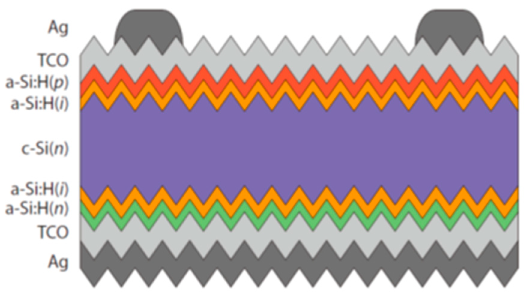
Since the 1980s, Sanyo Corporation, which was subsequently acquired by Panasonic Corporation, has been in the leading position in the SHJ solar cell industry. The first a-Si:H/c-Si heterojunction solar cell was fabricated in 1983 [26,27,28]. The potential of heterojunction technology was demonstrated by Sanyo in 1992, with an intrinsic a-Si:H ultra-thin buffer layer between a doped emitter and c-Si wafer to reduce the interface state density, decrease surface recombination, and lower emitter saturation current, which was named HIT [26,27,28]. In SHJ solar cells, the emitter and back surface field are formed by doped a-Si:H films, sandwiching the c-Si wafer, among which an intrinsic a-Si:H buffer layer of a few nanometers in thickness is typically inserted between the c-Si surface and the doped a-Si:H films to further improve the passivation. That is to say, i-a-Si:H/n-a-Si:H are the electron-selective contacts, and i-a-Si:H/p-a-Si:H are the hole-selective contacts. Physically, the passivation stems from the hydrogenation of the c-Si surface states. The full c-Si area is passivated with the a-Si:H, and thus there is no direct contact between the c-Si absorber and the metal. Therefore, this approach has the potential to produce a very high Voc [26,27,28]. The silicon heterojunction structure suffers a lot from the a-Si:H/c-Si defects, as compared to the conventional homojunction structure. However, such a problem can be fixed by surface passivation techniques. When the a-Si:H layer is deposited onto the c-Si surface, not all the dangling bonds at the surface can be bonded because the a-Si:H network configuration is not always fit for bonding. As a result, these unpassivated dangling bonds lead to defects at the surface. Such a problem can be fixed by passivating those dangling bonds with hydrogen, which is also called chemical passivation. It is normally achieved by depositing a thin intrinsic a-Si:H layer. In addition, the passivation quality can be further improved by field-effect passivation, which is achieved by the deposition of the doped a-Si:H layer. Because of the fixed charge in the a-Si:H layer, the electric field is formed to force and accelerate the electron/hole separation in order to minimize recombination at the a-Si:H/c-Si interfaces [26,27,28].
From the cell fabrication process perspective, a-Si:H/c-Si heterojunctions have the following advantages over a conventional diffused-homojunction: (1) Excellent passivation properties, which achieve a high Voc and therefore a high efficiency; (2) low processing temperatures, which prevent bulk quality degradation in low-quality c-Si wafers; (3) a better temperature coefficient, compared to diffused-homojunction cells; and (4) a low-cost fabrication process, with a high potential for reducing production costs [26,27,28]. By the continuous optimization of the intrinsic a-Si:H passivation layer, back surface field and back-side passivation, highly conductive transparent ITO, texturing surface, metal grid lines, and wafer quality, Panasonic has increased its best cell efficiency to 24.7% on large areas [28]. The best Voc reached 750 mV, which was much higher than that of the state-of-the-art homojunction counterpart. Another prestigious Japanese corporation, Kaneka, reported an even higher efficiency of 25.1%, with a Voc of 738 mV, Jsc of 40.8 mA/cm2 and FF of 83.5% [19]. The schematic cross-section of a typical SHJ solar cell is shown in Figure 1.
Even though SHJ solar cells have reached very high efficiencies of around 25% [19,28], there are some disadvantages, most of which come from the front grid shading and parasitic absorption of front emitter layers, which ineluctably and severely decrease the current. Additionally, the problem of how to balance the series resistance and anti-reflection properties of the front TCO presents another limitation.
For the interdigitated back contacted (IBC) solar cell, both the emitter and the base contact are placed at the back surface to form an interdigitated structure [62]. Since there are no emitter contacts on the front side, more light can penetrate into the absorptive c-Si wafer. Additionally, the original emitter contact area at the front can be coated by passivation and anti-reflection layers, which can lead to a further current increase. SunPower Corporation has been the leader in the industry for a number of years, with its renowned IBC solar cell efficiency of up to 25% [17]. By combining the SHJ and IBC structures, a novel IBC-SHJ solar cell is formed, which provides both a high Voc of the SHJ solar cell and a high Jsc of the IBC solar cell [18,20,21]. The IBC-SHJ solar cell is considered the most promising to approach the theoretical limit efficiency of a c-Si solar cell [20,63]. Based on this novel and promising structure, Panasonic Corporation achieved a high efficiency of 25.6% (Voc = 740 mV, FF = 82.7%, Jsc = 41.8 mA/cm2, 143.7 cm2) [18], whilst Kaneka Corporation reported an even higher efficiency of 26.6% (Voc = 740 mV, FF = 84.6%, Jsc = 42.5 mA/cm2, 179.7 cm2) [20,21].
2.2. Tunnel Oxide Passivated Contact (TOPCon) Solar Cells
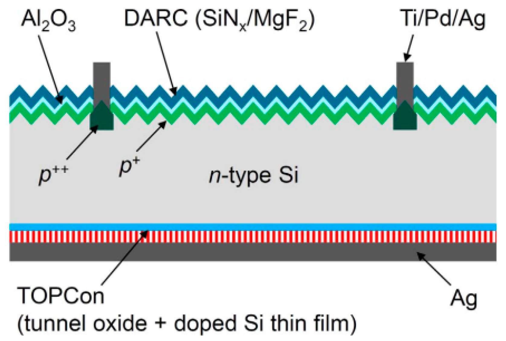
Only a small area on the rear side is contacted in order to reduce recombination with PERC technology, although additional patterning steps are still required, leading to longer current conduction paths in the c-Si wafer [6,7]. In 2014, Fraunhofer ISE proposed a full-area, carrier-selective, passivated contact as an appealing alternative to a partial rear contact, and named it Tunnel Oxide Passivated Contact (TOPCon) [64], which consists of metal contacts on both the front and back sides and removes patterning from the back side by full-area passivated back contacts [22,23,64]. This has served the purpose both of increasing efficiencies and simplifying the manufacturing processes. The thickness of the intermediate SiO2 passivation layer is reduced to one or two nanometers, allowing the charge carriers to ‘tunnel’ through it. Subsequently, a thin coating of highly doped silicon is deposited over the entire layer of the ultra-thin tunnel oxide. This novel combination of layers allows the electrical current to flow out of the cell with nearly zero loss. The structure of the TOPCon solar cell is shown in Figure 2. The first key technical issue of the TOPCon technology is the preparation of the ultra-thin oxide layers, which was previously realized by wet chemical methods by Fraunhofer ISE. Later, researchers developed various methods to prepare ultra-thin oxide layers [65,66], including plasma-assisted oxidation, wet chemical hydrochloric acid oxidation, wet chemical nitric acid oxidation, thermal oxidation, and UV/O3 anodization. Secondly, the as-deposited doped silicon thin layer is amorphous. A post-annealing process is usually needed to increase the crystallization fraction [64] and activate the dopant, leading to the excellent field passivation and junction property. Low-pressure chemical vapor deposition (LPCVD) [67] or Ion implantation [68,69] were also performed to achieve heavily-doped poly-Si films.
Compared with the PERC cell, the TOPCon cell provides a simple rear contact, without any patterning, reducing the costs and process complexity. Additionally, the quality of the c-S wafer is essential for a highly efficient solar cell [64,65,66,67,68,69]. For solar cells with pronounced lateral structures (PERC, IBC), only c-S wafers with certain base resistances can lead to high efficiencies. On the contrary, due to the one-dimensional current flow in the TOPCon solar cell, the base resistance has no significant influence on the solar cell performance. High Voc (>715 mV), high FF (>81.5%) and high efficiencies were achieved for c-S wafers, with a wide base resistance between 1 and 10 Ωcm. Using the TOPCon back side structure, a record efficiency of 25.7% (Voc = 725 mV, FF = 83.3% and Jsc = 42.5 mA/cm2) could be achieved, with a low resistivity of 1 Ωcm for n-type c-Si [23]. This represents the highest efficiency reported for both-sides contacted c-Si solar cells.
2.3. Polycrystalline Silicon on Oxide (POLO) Solar Cells
IBC-SHJ solar cells held the record efficiency of 26.6% [21], although they suffer from the inherent limitations of low-temperature processing. Thus, low-temperature metallization and interconnection procedures need to be developed. The other disadvantage is parasitic optical absorption in the doped a-Si:H layer and the need for ultra-clean wafer surfaces before the deposition of thin-film silicon layers. Combining heterojunction with back-contacted structures also requires complex patterning procedures in the formation of interdigitated junctions. In an effort to address these limitations, ISFH has developed polycrystalline silicon on oxide (POLO) passivating contacts, which are stable under high temperatures [24,25,72]. The crucial aspects of the POLO contacts are the growth of interfacial oxide and deposition of intrinsic polycrystalline silicon layers, which are subsequently doped. The beauty of the approach is that the resultant junctions have a low recombination current density (1 fA/cm2 on n+-POLO and 4 fA/cm2 on p+-POLO), which can be contacted by metal without inducing any additional recombination losses. For this kind of back-contact technology, it is necessary to separate the base and emitter regions. ISFH employed textured trenches to separate evaporated aluminum contacts. The interfacial oxide can be grown thermally or by means of wet chemistry. Commercially available LPCVD systems are employed to deposit intrinsic polycrystalline silicon layers. The intrinsic layers are subsequently doped using an ion implantation process, while in-situ doping in LPCVD is also possible.
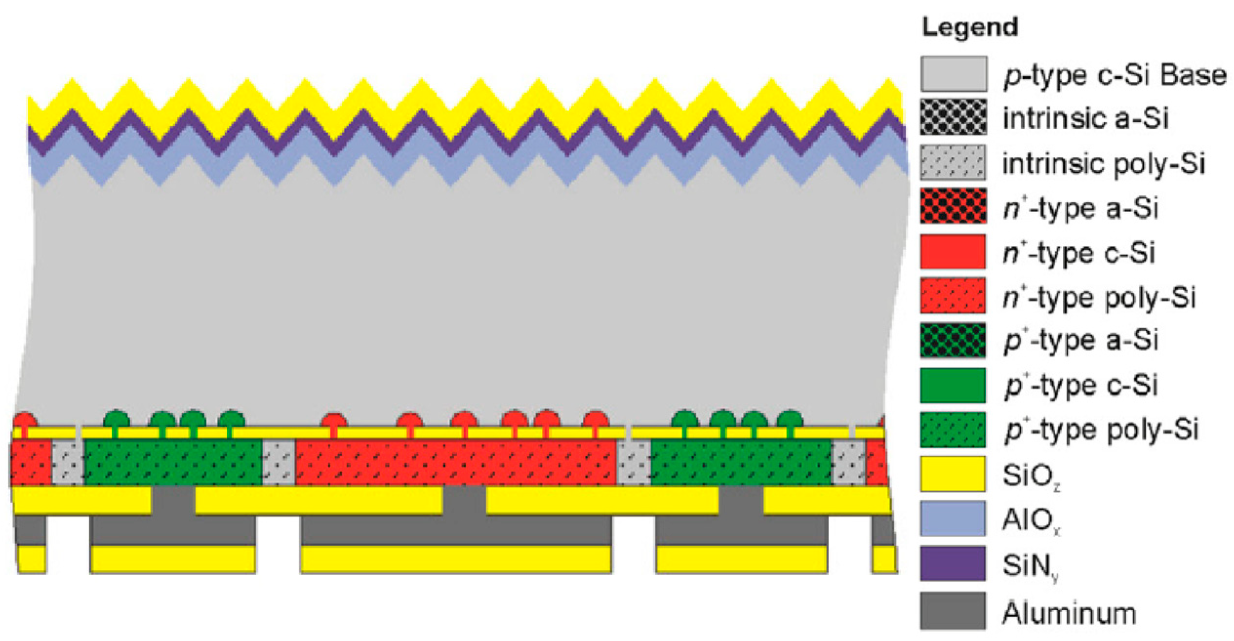
Compared with the a-Si/c-Si heterojunction, the poly-Si/c-Si junction has a lower saturation current density, a lower contact resistance, and better carrier selectivity [73]. In addition, polycrystalline silicon has a very high defect state, but when used in a POLO solar cell as a back contact, the recombination of such a PN junction is greatly reduced [74]. Subsequently, by comparing the same thickness of a p-type a-Si:H layer and p-type poly-Si layer, Reiter et al. found that the former has a higher loss of short-circuit current density due to parasitic absorption [75]. They also conducted related studies on the mechanism of carrier selectivity in poly-Si/c-Si junctions. They found that n+-poly-Si behaves better in terms of electron selectivity, while p+-poly-Si demonstrates an excellent hole selectivity. Chemically etched grooves were used to separate the n+-poly-Si and p+-poly-Si, which were combined with the interfacial silicon oxide to obtain excellent passivation [76]. Adapting the POLO concept to the back-contact architecture, as shown in Figure 3, ISFH attained an impressive 26.1% efficiency in February 2018, which is the record efficiency for a p-type c-Si wafer solar cell [25].
A photolithography-free process sequence for POLO technology, adapted to a back-contact structure on n-type c-Si wafers, has also been developed. This approach also relies on textured trenches to separate the emitter and base regions and employs inkjet and laser technology for patterning and contact opening, a mask-free high throughput metallization process, and a self-aligned contact separation method. A high efficiency of 24.25% was obtained for n-type c-Si wafers [77].
3. Dopant-Free Carrier-Selective Contacts
Compared to the doped silicon films, dopant-free carrier-selective contacts consist of elementary or compound thin films, with high work functions as hole-selective contacts and low work functions as electron-selective contacts. For example, electron-selective contacts include compounds with a low work function, such as LiFx [30,32,40], MgFx [56], TiO2 [31,40,43,44,45] and ZnO [46,47], and alkaline metals with an extremely low work function, such as Mg [54] and Ca [57]. Hole-selective contacts mainly consist of organic films [48,49,50,51,52,53] and transition metal oxides (TMOs), such as MoOx [30,32,36,37,38,40,41,42,47], WOx [35,38,39], V2Ox [33,34,35,38], and NiOx [31].
3.1. PEDOT:PSS Hole-Selective Contacts
In order to form organic/c-Si heterocontacts for hole-selectivity, a wide range of organic layers are investigated, including TAPC [48], Spiro-OMeTAD [49], and PEDOT:PSS [50,51,52,53], among which PEDOT:PSS remains the most promising candidate.
Since it is difficult to successfully form uniform PEDOT:PSS layers on textured c-Si wafers, conventional n-Si/PEDOT:PSS solar cells are generally fabricated on planar c-Si substrates, which usually have relatively high reflectivity and poor current density. He et al. firstly deposited PEDOT:PSS layers on textured c-Si and then fabricated a water-insoluble phthalic acid ester, diethyl phthalate (DEP), onto the PEDOT:PSS. The external tensile stress stretches the PEDOT:PSS films so that they have a tight contact with the textured c-Si surface, even at the valley regions, which largely decreases the pyramid-textured c-Si/PEDOT:PSS interface recombination. Because of the improved electrical passivation, the enlarged junction area, as well as the excellent light trapping property, a high efficiency of up to 16.2% was obtained [51].
If the PEDOT:PSS layer is deposited on the front side of a solar cell, a significant parasitic light absorption within the PEDOT:PSS layer is inevitable. Zielke et al. proposed a back-junction organic-silicon solar cell, in which the PEDOT:PSS layer was placed on the rear side instead of the front surface to avoid parasitic light absorption within the PEDOT:PSS and to allow for an improved surface passivation. This novel solar cell was named the “BackPEDOT” cell [52]. By optimizing the silicon surface pre-treatment in combination with the adapted PEDOT:PSS blend, record efficiencies of 18.3% and of 20.6% were achieved for n-type c-Si and p-type c-Si wafers, respectively [53].
3.2. Alkali/Alkaline Earth Metal Salts Electron-Selective Contacts
Inherited from the organic electronic community, thin alkali and alkaline earth metal salt interlayers, including LiFx [30,32,40], MgFx [56], Mg [54] and Ca [57], can be used to enhance electron extraction, and when these layers are integrated under a metal electrode, low work function values can be obtained (as low as ~2.5 eV, in some cases), promoting electron collection from the adjacent c-Si surface. In fact, alkali and/or alkaline earth metal salts have been explored intensively as electrodes with low work functions in solar cells and light-emitting diodes.
Due to the ubiquitous Fermi-level pinning effect, the low-resistance contact between metals and lightly-doped n-type c-Si is a technologically challenging issue, which usually results in a relatively high Schottky barrier (>0.65 eV) for electrons. Bullock developed a simple and robust process to reduce the impact of contact recombination and optical losses, and also to achieve an mΩcm2 scale contact resistivity on lightly-doped n-type c-Si via a lithium fluoride/aluminum (LiF/Al) partial rear contact, permitting a conversion efficiency higher than 20% in the initial proof-of-concept stage [55]. In 2016, Bullock successfully developed and implemented dopant-free electron-selective heterocontacts, using alkali metal fluorides in combination with passivating intrinsic a-Si:H interlayers, resulting in a conversion efficiency of 19.42% for a DASH cell [30].
Magnesium fluoride (MgF2), an alkaline earth metal salt, has a long history of being utilized as an antireflection coating in optical devices, including c-Si solar cells, because of its high transparency and low refractive index (n ≈ 1.36). Wan investigated the conduction and recombination properties of a thermally-evaporated MgF2/Al electron−selective contact on n-type c-Si for the first time. A significantly lower work function than that of pure aluminum was obtained. Application of the novel electron contact to the full rear surface of n-type c-Si solar cells resulted in a conversion efficiency of over 20% [56].
Allen demonstrated a low resistance Ohmic contact for n-type c-Si wafers by incorporating a metal calcium (ϕ~2.9 eV) layer with a low work function between c-Si and an aluminum electrode. Contact resistivity (ρc) of ~2 mΩcm2 can be realized on undiffused n-type silicon, thus enabling partial rear contact cell designs on n-type c-S, without the need for a phosphorus diffusion. Integrating the Ca/Al stack into a partial rear contact solar cell architecture, fabricated on a lightly-doped (ND = 4.5 × 1015 cm−3) n-type wafer, resulted in a device efficiency of 20.3%, whereas the Ca/Al contact comprised only ~1.26% of the rear surface [57]. Tong reported a high-performance electron-selective contact by combining an ultrathin SiOx and an Mg layer with a low work function, which simultaneously achieved moderate-level passivation and low contact resistivity on lightly-doped n-type c-Si. In addition, the deposition of Mg on SiOx relaxes the restriction on the threshold thickness of the SiOx for electron tunneling and therefore broadens the optimization space for rear-sided passivation [54]. A dopant-free c-Si solar cell, with a SiOx/low-WFM electron-selective contact and a MoOx hole-selective contact, yielded a high efficiency of 21.8% [58].
3.3. Transition Metal Oxide (TMO) Carrier-Selective Contacts
Transition-metal-oxides (TMO) are of great interest since they are cheap, non-toxic, and abundant. They usually demonstrate large band gaps (Eg > 3 eV), a wide variety of work functions, from 3 to 7 eV, and conductivities, from insulating to metallic-like, which make them highly flexible when used as electron- or hole-selective contact materials [78]. In addition, these films can be deposited at low temperatures (T < 200 °C), or by solution-processing methods [42,79], indicating a greater potential for process simplification and cost reduction.
If both the dopant-free hole and electron-selective contacts are deposited on the front and rear sides of c-Si wafers, respectively, these novel devices are nominated as dopant-free asymmetric heterocontacts (DASH) solar cells [30,40], which have been widely investigated in recent years and will be one of the most promising key issues for further improving the performance of c-Si-based solar cells. The DASH solar cells, based on TMOs, have the following advantages [30,31,32,33,34,35,36,37,38,39,40,41,42,43,44,45,46,47]: (1) TMOs have a large band gap and thus low parasitic light absorption, which is beneficial for increasing the short-circuit current density of the solar cell; (2) the DASH solar cell has a very high efficiency potential of up to 28% [31]; (3) most of the TMOs can be deposited by low-temperature and low-cost techniques, such as thermal evaporation or the solution method; (4) no flammable, explosive, or toxic gases and materials are used; (5) it is easy to realize the IBC structure by multi-step masks, which avoids the complicated photolithography processes [32,33,34].
3.3.1. TMO Hole-Selective Contacts
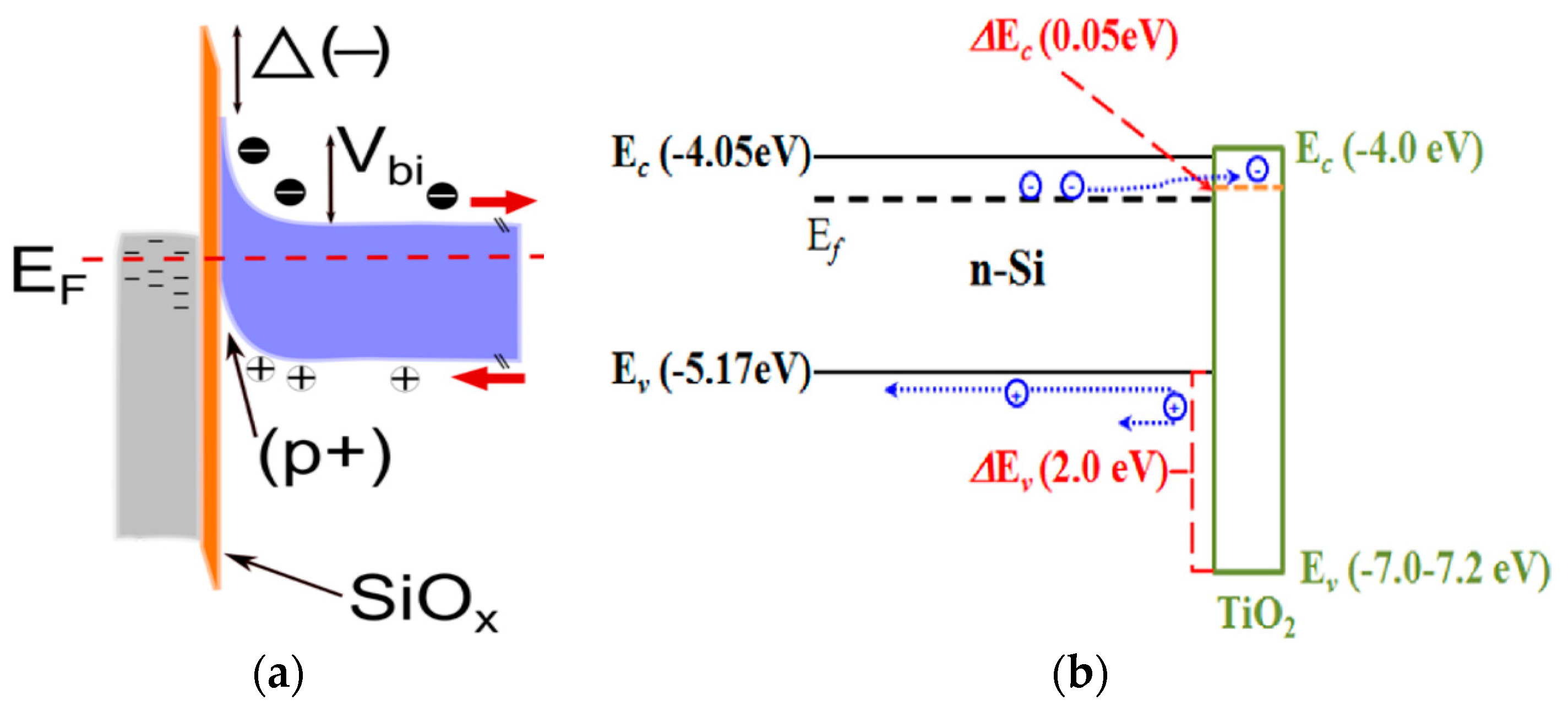
The most commonly used TMO materials as hole-selective contacts are MoOx, V2Ox, and WOx. These materials exhibit an n-type nature, although their work functions are as high as ~6.0 eV, indicating much lower Fermi levels than those of n-type c-Si. When these TMOs are connected with c-Si, the Fermi levels in these two materials are aligned and cause an energy band bending of about 0.8 eV on the c-Si surface, which is similar to the value caused by the p-type a-Si:H layer. From a band alignment perspective, a large conduction band offset will be formed on the Si surface, leading to a strong inversion layer with an accumulation of holes. The heterojunction works more like a p-n junction and enables a high enough theoretical built-in potential [30]. This behavior lays the foundation for the high efficiency of TMO/c-Si solar cells. A schematic diagram of the energy band of the MoOx/c-Si interface is shown in Figure 4a.
MoOx is the most explored hole-selective contact material at present [30,32,36,37,38,40,41,42,47]. In 2014, Battaglia deposited 15 nm MoOx directly on the n-type c-Si by thermal evaporation as a hole-selective contact, achieving a cell efficiency of 14.3% [36]. In 2015, Geissbühler replaced the p+-a-Si:H emitter in a conventional SHJ solar cell using MoOx as a hole-selective layer, reaching a conversion efficiency of 22.5% in a MoO3/(i)a-Si:H/n-Si configuration [37], in which the intrinsic a-Si:H chemically passivates the silicon surface while the MoO3 provides the hole-selectivity. In 2016, Bullock used intrinsic a-Si:H as the passivation layers, MoOx as the hole-selective contact, and LiFx as electron-selective contact, respectively. A Voc of 714 mV and efficiency of 19.4% were achieved with this structure [30]. Additionally, rear MoOx contacts with partial contact areas have been reported with an efficiency of 20.4% for the p-type c-Si wafer [80].
Gerling [38] and Wu [39] compared the effects of the V2Ox, MoOx, and WOx hole-selective contacts on the SHJ solar cells, reaching a conclusion that V2Ox is a better candidate for the hole-selective contact. Shen and co-workers proposed a multi-layered emitter (i.e., hole-selective contact) based on a TMO/Ag/TMO structure [33,81]. The first TMO layer to make contact with c-Si caused band bending on the c-Si surface, achieving carrier selectivity. The Ag layer, with a thickness of only a few nanometers, improves the overall conductivity of the multilayer structure. The second TMO layer is used for anti-reflection and carrier collection. Therefore, the TMO/Ag/TMO multi-layered emitter greatly reduced the sheet resistance and simultaneously acted as the hole-selective contact and the transparent conductive electrode. With a V2Ox/Ag/V2Ox hole-selective contact, the cell efficiency with the IBC structure reached 19.02% [39]. Masmitjà used V2Ox as the single-layer hole-selective contact and achieved an efficiency of 19.1% [34]. The above results show the great potential of V2Ox as an effective hole-selective contact.
3.3.2. TMO Electron-Selective Contacts
Metal oxides with a low work function and small conduction band offset with n-Si are promising candidates for insertion between the Si/Al interface in order to alleviate the Fermi level pinning effect and reduce the energy barrier for electrons. For example, the TiOx/Si interface has been demonstrated to have a small conduction band offset (ΔEc~0.05 eV) and a high valence band (ΔEv~2.0 eV), which would allow the transport of electrons from silicon to TiOx and a large valence band offset, and block the holes from silicon to TiOx, as illuminated in Figure 4b [43].
Yang has studied the effect of different contacts on electron transport in n-type c-Si solar cells. The use of a double-layer structure of SiO2/TiO2 can improve the passivation and increase the cell efficiency to 22.1% [44]. Applying MoOx as a hole-selective contact layer and LiFx as an electron-selective contact layer, as well as intrinsic a-Si:H as passivation layers, on both the front and back sides of c-Si wafers, Bullock et al. reported a novel DASH solar cell with an efficiency of 19.4% [30]. Further inserting an ultrathin TiOx to form a TiOx/LiFx hybrid electron-selective contact, the cell efficiency was improved to 20.7% [40]. Sun compared the difference between the heterojunction, formed by ZnO/c-Si and TiO2/c-Si. The TiO2 not only realize the electron selectivity, but also passivate the c-Si surface [82], which can contribute to the formation of Si-O-Ti bonds. ZnO has a very similar band structure as TiO2, although ZnO cannot form similar bonds and does not play a role in the passivation. Finally, when TiO2 was used as an electron-selective contact, the corresponding solar cell demonstrated a Voc of 643 mV and FF of 72.4%, while a Voc of 637 mV and FF of 75.2% were obtained for the ZnO electron-selective contact [82]. Ye and Gao’s group directly deposited titanium film on an n-type c-Si of 8 Ω·cm by electron beam evaporation, which was then annealed at 250 °C in an oxygen atmosphere to form TiO2. The surface recombination rate can be reduced to 16 cm/s, showing an excellent passivation quality, which was attributed to the formation of Si-O-Ti bonds at the c-Si/TiO2 interface and the chemical passivation of the SiO2 [83]. By using a metal with an extremely low work function such as Mg and SiO2 as the full-area electron selective contacts, the contact resistance and recombination current density were reduced to 26 mΩcm2 and 115 fA/cm2, respectively [54]. In contrast, Khan et al. showed that the silver-doped aluminum-rich zinc oxide (ZnO:Al:Ag), prepared by the sol-gel method, provided a significant passivation of the n-Si. The minority carrier lifetime reached 1581.2 μs, and Voc reached 688.1 mV. This passivation was attributed to the chemical passivation of the naturally formed SiOx during the preparation of ZnO:Al:Ag, and to the field effect passivation caused by charges at the ZnO/Si interface [46].
Wan et al. demonstrated a highly conductive and thermally-stable electrode composed of a magnesium oxide/aluminum (MgOx/Al) contact, achieving moderately low resistivity ohmic contacts on lightly-doped n-type c-Si. The electrode, functionalized with nanoscale MgOx films, significantly enhances the performance of n-type c-Si solar cells to a power conversion efficiency of 20%, advancing n-type c-Si solar cells with full-area dopant-free rear contacts [84,85].
Wang et al. used MoOx and ZnO:B as the hole- and electron-selective contacts, with the structure of MoOx/i-a-Si:H/n-c-Si/i-a-Si:H/ZnO:B, and obtained a cell efficiency of 16.6% [47]. ZnO:B, as the electron-selective contact, has two significant advantages: First, its lower refractive index enhances the back-reflection and significantly improves the spectral response in the long wavelength range, from 900 nm–1200 nm. Secondly, its good conductivity lowers the contact resistance, and the fill factor is significantly improved.
3.3.3. TMO/c-Si Interface Passivation Layers
The lattice mismatch between TMO and c-Si inevitably results in a high defect density and consequently in a high carrier recombination at the contact interface, which can be reduced by inserting an ultrathin dielectric interlayer between the c-Si surface and the contacting metal, which is called “passivated contact”. The ultra-thin dielectric layers simultaneously play three roles, including separating metal from the silicon wafer, passivating the silicon surface, and serving as a contact to the solar cell. Until now, ultra-thin SiO2, Al2O3, and a-Si:H dielectrics have frequently been investigated and applied as passivated contact layers for c-Si solar cells [36,37,41,64,65,66,67,68,73,76]. However, they still suffer from an increased contact resistivity (ρc) between the c-Si wafer and the carrier-selective contact layer. Because of its wide band gap, SiOx has a stronger hole blocking capability, compared to TiOx and intrinsic a-Si:H. A tunnelable SiOx interlayer may alleviate ρc in SiOx-based electron-selective contacts, but the critical thickness for electron tunneling may not allow for satisfactory c-Si surface passivation. From the results of an intrinsic a-Si:H layer for SHJ solar cells and a SiO2 layer for TOPCon and POLO solar cells, the typical thickness of an intrinsic a-Si:H layer is around 4–5 nm [18,19,20,21,26,27,28], while it is about 1.5 ± 0.5 nm for SiO2 layers [22,23,24,25,64,65,66,67,68,69,70,71,72,73,74,75,76,77], i.e., effective interface passivation layers. Thicker layers result in a better passivation quality and high contact resistivity, while a poor passivation quality and low contact resistivity are the characteristics of thinner layers.
Battaglia’s research indicated that an MoOx/c-Si heterojunction solar cell, without any passivation layer, achieved an efficiency of only 14.3%, and the Voc was as low as 580 mV [36]. If an intrinsic a-Si:H passivation layer was adopted to form the MoOx/a-Si:H/c-Si solar cell, the Voc was improved to 711 mV, and the cell efficiency was 18.8% [41]. Geissbühler showed that when replacing the p-type a-Si:H film with an MoOx layer at the front of SHJ solar cells, with an intrinsic a-Si:H passivation layer between an MoOx layer and c-Si wafer, a high efficiency of 22.5%, with a high Voc of 725.4 mV is demonstrated. These results demonstrate that an MoOx layer can be an effective and efficient hole-selective contact, and that excellent passivation properties can be achieved on intrinsic a-Si:H layers [37].
According to the research of Gerling [38], Khan [46], and Tong [42], it was found that naturally formed SiOx on the c-Si surface during the MoOx deposition by the thermal evaporation or solution method plays a key role in the c-Si surface passivation. However, the naturally formed SiOx is not compact enough to provide enough passivation. Therefore, an extra well-designed process is needed to obtain a compact SiOx passivation layer. Since SiOx passivation layers, obtained by ozone oxidation, concentrated nitric acid oxidation, and H2O2 oxidation in high-efficiency TOPCon solar cells [65,66] have been successfully applied, these methods used for compact SiOx passivation layers could be imitated in order to improve the performance of DASH solar cells. What is more, Masmitjà used 0.5 nm ultra-thin Al2O3, deposited by atomic layer deposition at the TiO2/c-Si interface, as the passivation layer. The surface recombination rate was reduced to 33 cm/s, and the corresponding implied Voc reached 680 mV [34].
3.3.4. High-Efficiency DASH Solar Cells
Imran’s numerical simulation indicated the theoretical efficiency for a both-sides contacted DASH solar cell, with metal oxide layers on the front and back sides of a c-Si wafer as hole- and electron-selective contacts, respectively, which can be as high as 28%, with a Voc of 772.7 mV, Jsc of 43.63 mA/cm2 and FF of 82.99% [31]. If the IBC structure is further adopted, an even higher efficiency can be expected.
Current experimentally-reported DASH solar cells based on TMO usually adopt a both-sides contacted front-junction structure [30,31,35,36,37,38,40,41,42,43,44,45,46,47]. The c-Si solar cell, with only MoOx as the hole-selective contact, which has a structure of ITO/MoOx/i-a-Si:H/c-Si/i-a-Si:H/n-a-Si:H/Al, demonstrated a record conversion efficiency of 22.5%, compared with the current TMO-based solar cells [37]. If both hole- and electron-selective contacts were made of dopant-free TMO materials, the current highest conversion efficiency is 20.7%, with a structure of TCO/MoOx/i-a-Si:H/c-Si/i-a-Si:H/TiOx/LiF/Al, of which the structure, J–V curve, external quantum efficiency, internal quantum efficiency, and reflection are shown in Figure 5 [40].
In order to further improve the utilization of incident light, inspired by the SunPower’s IBC solar cell, Um [32], Wu [33,39] and Masmitjà [34] placed both hole- and electron-selective contacts on the back side of the c-Si wafers to realize the full-back-contacted solar cells, with corresponding conversion efficiencies of 15.4%, 19.02%, and 19.7%, respectively. The conversion efficiencies of these IBC-structured solar cells do not exceed those of the both-sides contacted ones, although the low-temperature deposition and metal patterning techniques, together with the simplicity of the devices themselves, still suggest the great potential of low-cost and high-efficiency all-back-contact c-Si solar cells using structured and dopant-free carrier-selective contacts.
3.4. Working Mechanisms of TMO/c-Si Solar Cells
3.4.1. Carrier Separation
In a conventional PN junction, the built-in potential is considered the internal force to separate the photogenerated carriers. However, current research suggests that the PN junction is not necessary for a solar cell, while the asymmetric conductivity of the contact layers on the two sides of the absorber layer is the internal force that promotes the separation of photogenerated carriers [86,87]. As a new type of solar cell, which has just been developed in recent years, the basic physical principles of the internal force of carrier separation in c-Si DASH solar cells have not been clearly understood [60,61], even though their conversion efficiencies are higher than 20% [40].
Gerling regarded the difference between TMO’s high work function and the n-Si Fermi level to be the driving force behind the balance of Fermi levels [38]. Carrier selectivity is controlled by the band bending induced by n-Si. The difference (~1.2 eV) between the work function of TMO and the Fermi level of n-Si cannot meet the needs for Fermi level balance. A negatively charged dipole should exist at the TMO/n-Si interface, which results in a shift of the energy band and makes the carrier transport more complicated. He thought that, in this kind of cell, there was no band bending in MoOx, and all the depletion regions are in c-Si. However, Battaglia considered that MoOx in MoOx/c-Si cells behave more like the high-work function metal. Band bending occurs on both the c-Si surface and the MoOx [36,41]. Sun studied the band alignment of MoOx/n-Si by UPS and XPS and found that there are interfacial dipoles (~0.97 eV), which are related to energy band bending (~0.80 eV) on both sides of the interface [82].
3.4.2. Carrier Transport
Battaglia compared the band diagram of the heterojunction of MoOx/n-Si and p-type a-Si:H/n-Si. The common features of these two heterocontacts are inversion layers, formed on the n-Si surface. The band bending of n-Si and the offset in the conduction band between n-Si and a-Si:H together cause a large barrier to electron transport. In both cases, MoOx and p-type a-Si:H can provide similar hole extraction conditions: The holes firstly pass over the barrier, formed by the valence band offset between n-Si and a-Si:H, and then pass through the tail states in a-Si:H or the oxygen vacancies in MoOx, eventually reaching the ITO front electrodes [36,41].
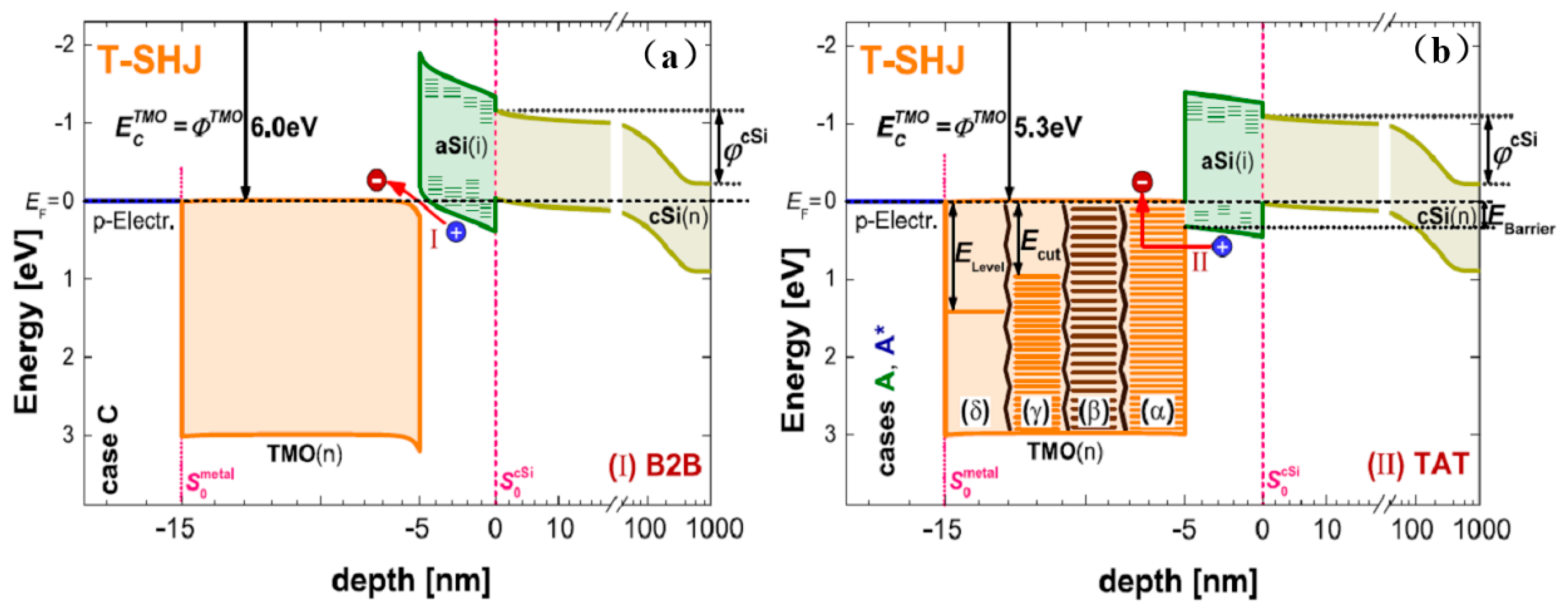
Vijayan [87] and Messmer [88] studied the hole transport paths at the TMO/Si interface by simulations. They held similar ideas that there are two possible paths, including band-to-band tunneling (B2B) and defect-assisted tunneling (TAT), depending on the electron affinity of TMO. As shown in Figure 6, if TMO has a sufficiently large electron affinity (i.e., a high work function), which makes the conduction band of TMO lower than the valence band of c-Si, the band-to-band tunneling is the main transport mechanism. If the electron affinity of TMO is small (i.e., the work function is low), defect-assisted tunneling via TMO’s bulk defects is necessary, which may result in additional series resistance. If the electron affinity is further decreased, and the defect states in the TMO are insufficient, the J–V curve will behave as the S-shape. These results further indicate that the high work function (electron affinity) of TMO is critical to improving the performance of TMO/Si solar cells. However, the above-mentioned results from the simulation need to be verified by experimental results concerning solar cells.
4. Summary and Outlook
This article presents the latest advances in highly efficient c-Si solar cells with passivation contacts, including doped silicon films and dopant-free materials, with a high/low work function. Since the IBC structure is proven to be an effective and efficient way work to improve the short-circuit current density, the combination of carrier-selection, passivation contact, and IBC structure will be the inevitable route to the achievement of a higher conversion efficiency. The next step of research should also focus on the optimization of existing carrier-selective materials and contact structure, exploitation of novel contact and interfacial passivation materials, low-cost deposition techniques, novel device design, and further understanding of device physics.
Additionally, besides the wide investigations on SHJ solar cells, the TMOs with a high/low work functions have critical applications in perovskite solar cells, which are one of today’s most promising up-and-coming photovoltaic technologies [89,90,91,92]. Over the past decades, in order to overcome the single-junction limit of silicon solar cells [93], the so-called “third-generation photovoltaics” concepts [9] were proposed, of which the multi-junction PV device is proven to be an efficient and effective one. In fact, recent two-terminal tandem devices consisting of a perovskite top cell and SHJ bottom cell have reached very promising efficiencies [94,95,96], of which the SHJ bottom cell includes two-side doped silicon thin-film passivation contacts. The TMOs prepared by the solution method are compatible with the fabrication processes of perovskite solar cells, which facilitates the realization of a good tunneling junction between the top and bottom cells, an all solution-processed fabrication and, finally, highly efficient perovskite/Si tandem solar cells.
Author Contributions
Writing—Original Draft Preparation, C.Y.; Writing—Review & Editing, S.X., J.Y. and S.H.
Funding
This research was funded by the National Natural Science Foundation of China (No. 61474066, 61504069) and the Natural Science Foundation of Tianjin (No. 15JCYBJC21200).
Conflicts of Interest
The authors declare no conflict of interest. The founding sponsors had no role in the design of the study; in the collection, analyses, or interpretation of data; in the writing of the manuscript, and in the decision to publish the results.
References
- Zheng, C.; Kammen, D.M. An innovation-focused roadmap for a sustainable global photovoltaic industry. Energy Policy 2014, 67, 159–169. [Google Scholar] [CrossRef]
- Louwen, A.; van Sark, W.G.J.H.M.; Faaij, A.P.C.; Schropp, R.E.I. Re-assessment of net energy production and greenhouse gas emissions avoidance after 40 years of photovoltaics development. Nat. Commun. 2016, 7, 13728. [Google Scholar] [CrossRef] [PubMed] [Green Version]
- Hou, G.; Sun, H.; Jiang, Z.; Pan, Z.; Wang, Y.; Zhang, X.; Zhao, Y.; Yao, Q. Life cycle assessment of grid-connected photovoltaic power generation from crystalline silicon solar modules in China. Appl. Energy 2016, 164, 882–890. [Google Scholar] [CrossRef]
- Web Site of Fraunhofer ISE. Available online: https://www.ise.fraunhofer.de/content/dam/ise/de/documents/publications/studies/Photovoltaics-Report.pdf (accessed on 9 September 2018).
- Chapin, D.M.; Fuller, C.S.; Pearson, G.L. A new silicon p-n junction photocell for converting solar radiation into electrical power. J. Appl. Phys. 1954, 25, 676–677. [Google Scholar] [CrossRef]
- Zhao, J.; Wang, A.; Green, M.A. 24.5% Efficiency Silicon PERT Cells on MCZ Substrates and 24.7% Efficiency PERL Cells on FZ Substrates. Prog. Photovolt. Res. Appl. 1999, 7, 471–474. [Google Scholar] [CrossRef]
- Green, M.A. The path to 25% silicon solar cell efficiency: History of silicon cell evolution. Prog. Photovolt. Res. Appl. 2009, 17, 183–189. [Google Scholar] [CrossRef] [Green Version]
- Zhao, J.; Wang, A.; Green, M.A. Green High-efficiency PERL and PERT silicon solar cells on FZ and MCZ substrates. Sol. Energy Mater. Sol. Cells 2001, 4, 429–435. [Google Scholar] [CrossRef]
- Liu, J.; Yao, Y.; Xiao, S.; Gu, X. Review of status developments of high-efficiency crystalline silicon solar cells. J. Phys. D Appl. Phys. 2018, 51, 123001. [Google Scholar] [CrossRef] [Green Version]
- Battaglia, C.; Cuevas, A.; De Wolf, S. High-efficiency crystalline silicon solar cells: Status and perspectives. Energy Environ. Sci. 2016, 9, 1552–1576. [Google Scholar] [CrossRef]
- Abdullah, M.F.; Alghoul, M.A.; Naser, H.; Asim, N.; Ahmadi, S.; Yatim, B.; Sopian, K. Research and development efforts on texturization to reduce the optical losses at front surface of silicon solar cell. Renew. Sustain. Energy Rev. 2016, 66, 380–398. [Google Scholar] [CrossRef]
- Feldmann, F.; Simon, M.; Bivour, M.; Reichel, C.; Hermle, M.; Glunz, S.W. Carrier-selective contacts for Si solar cells. Appl. Phys. Lett. 2014, 104, 181105. [Google Scholar] [CrossRef]
- Hermle, M.; Schneiderlöchner, E.; Grupp, G.; Glunz, S.W. Comprehensive comparison of different rear side contacting methods for high-efficiency solar cells. In Proceedings of the 20th European Photovoltaic Solar Energy Conference, Barcelona, Spain, 6–10 June 2005; pp. 810–813. [Google Scholar]
- Xiao, Y.-P.; Gao, C.; Wang, T.; Zhou, L. Carrier selective contacts: A selection of high efficiency silicon solar cells. Acta Phys. Sin. 2017, 66, 158801. [Google Scholar]
- Wang, L.; Lochtefeld, A.; Han, J.; Gerger, A.P.; Carroll, M.; Ji, J.; Lennon, A.; Li, H.; Opila, R.; Barnett, A. Development of a 16.8% efficient 18 µm silicon solar cell on steel. IEEE J. Photovolt. 2014, 4, 1397–1404. [Google Scholar] [CrossRef]
- Smith, D.D.; Cousins, P.; Westerberg, S.; De Jesus-Tabajonda, R.; Aniero, G.; Shen, Y.-C. Toward the Practical Limits of Silicon Solar Cells. IEEE J. Photovolt. 2014, 4, 1465–1469. [Google Scholar] [CrossRef]
- Masuko, K.; Shigematsu, M.; Hashiguchi, T.; Fujishima, D.; Kai, M.; Yoshimura, N.; Yamaguchi, T.; Ichihashi, Y.; Mishima, T.; Matsubara, M.; et al. Achievement of More than 25% Conversion Efficiency with Crystalline Silicon Heterojunction Solar Cell. IEEE J. Photovolt. 2014, 4, 1433–1435. [Google Scholar] [CrossRef]
- Adachi, D.; Hernández, J.L.; Yamamoto, K. Impact of carrier recombination on fill factor for large area heterojunction crystalline silicon solar cell with 25.1% efficiency. Appl. Phys. Lett. 2015, 107, 73–812. [Google Scholar] [CrossRef]
- Yoshikawa, K.; Kawasaki, H.; Yoshida, W.; Irie, T.; Konishi, K.; Nakano, K.; Uto, T.; Adachi, D.; Kanematsu, M.; Uzu, H.; et al. Silicon heterojunction solar cell with interdigitated back contacts for a photoconversion efficiency over 26%. Nat. Energy 2017, 2, 17032. [Google Scholar] [CrossRef]
- Yoshikawa, K.; Yoshida, W.; Irie, T.; Kawasaki, H.; Konishi, K.; Ishibashi, H.; Asatani, T.; Adachi, D.; Kanematsu, M.; Uzu, H.; et al. Exceeding conversion efficiency of 26% by heterojunction interdigitated back contact solar cell with thin film Si technology. Sol. Energy Mater. Sol. Cells 2017, 173, 37–42. [Google Scholar] [CrossRef]
- Glunz, S.W.; Feldmann, F.; Richter, A.; Bivour, M.; Reichel, C.; Steinkemper, H.; Benick, J.; Hermle, M. The irresistible charm of a simple current flow pattern—Approaching 25% with a solar cell featuring a full-area back contact. In Proceedings of the 31st European Photovoltaic Solar Energy Conference and Exhibition, EU PVSEC 2015, Hamburg, Germany, 14–18 September 2015. [Google Scholar] [CrossRef]
- Richter, A.; Benick, J.; Feldmann, F.; Fell, A.; Hermle, M.; Glunza, S.W. n-Type Si solar cells with passivating electron contact: Identifying sources for efficiency limitations by wafer thickness and resistivity variation. Sol. Energy Mater. Sol. Cells 2017, 173, 96–105. [Google Scholar] [CrossRef]
- Haase, F.; Kiefer, F.; Krugener, J.; Brendel, R.; Peibst, R. IBC Solar Cells with Polycrystalline on Oxide (POLO) Passivating Contacts for Both Polarities. In Proceedings of the 26th International Photovoltaic Science and Engineering Conference (PVSEC-26), Singapore, 24–28 October 2016. [Google Scholar]
- Haase, F.; Hollemann, C.; Schäfer, S.; Merkle, A.; Rienäcker, M.; Krügener, J.; Brendel, R.; Peibst, R. Laser contact openings for local poly-Si-metal contacts enabling 26.1%-efficient POLO-IBC solar cells. Sol. Energy Mater. Sol. Cells 2018, 186, 184–193. [Google Scholar] [CrossRef]
- Tanaka, M.; Taguchi, M.; Matsuyama, T.; Toru, S.; Shinya, T.; Shoichi, N.; Hiroshi, H.; Yukinori, K. Development of new a-Si/c-Si heterojunction solar cells: ACJ-SHJ (artificially constructed junction-heterojunction with intrinsic thin-layer). Jpn. J. Appl. Phys. 1992, 31, 3518–3522. [Google Scholar] [CrossRef]
- Fujishima, D.; Inoue, H.; Tsunomura, Y.; Asaumi, T.; Taira, S.; Kinoshita, T.; Taguchi, M.; Sakata, H.; Maruyama, E. High-performance HIT solar cells for thinner silicon wafers. In Proceedings of the 35th IEEE Photovoltaic Specialists Conference (PVSC), Honolulu, HI, USA, 20–25 June 2010; pp. 3137–3140. [Google Scholar] [CrossRef]
- Taguchi, M.; Yano, A.; Tohoda, S.; Matsuyama, K.; Nakamura, Y.; Nishiwaki, T.; Fujita, K.; Maruyama, E. 24.7% record efficiency SHJ solar cell on thin silicon wafer. IEEE J. Photovolt. 2014, 4, 96–99. [Google Scholar] [CrossRef]
- Stodolny, M.K.; Anker, J.; Geerligs, B.L.J.; Janssen, G.J.M.; van de Loo, B.W.H.; Melskens, J.; Santbergen, R.; Isabella, O.; Schmitz, J.; Lenes, M.; et al. Material properties of LPCVD processed n-type polysilicon passivating contacts and its application in PERPoly industrial bifacial solar cells. Energy Procedia 2017, 124, 635–642. [Google Scholar] [CrossRef]
- Bullock, J.; Hettick, M.; Geissbühler, J.; Ong, A.; Allen, T.; Sutter-Fella, C.; Chen, T.; Ota, H.; Schaler, E.; DeWolf, S.; et al. Efficient silicon solar cells with dopant-free asymmetric heterocontacts. Nat. Energy 2016, 1, 15031. [Google Scholar] [CrossRef]
- Imran, H.; Abdolkader, T.M.; Butt, N.Z. Carrier-Selective NiO/Si and TiO2/Si Contacts for Silicon Heterojunction Solar Cells. IEEE Trans. Electron Devices 2016, 63, 3584–3590. [Google Scholar] [CrossRef]
- Um, H.; Kim, N.; Lee, K.; Hwang, I.; Seo, J.; Seo, K. Dopant-free all-back-contact Si nanohole solar cells using MoOx and LiF films. Nano Lett. 2016, 16, 981–987. [Google Scholar] [CrossRef] [PubMed]
- Wu, W.; Lin, W.; Bao, J.; Liu, Z.; Liu, B.; Qiu, K.; Chen, Y.; Shen, H. Dopant-free multilayer back contact silicon solar cells employing V2Ox/metal/V2Ox as an emitter. RSC Adv. 2017, 7, 23851–23858. [Google Scholar] [CrossRef]
- Masmitja, G.; Gerling, L.G.; Ortega, P.; Puigdollers, J.; Martin, I.; Voz, C.; Alcubilla, R. V2Ox-based hole-selective contacts for c-Si interdigitated back-contacted solar cells. J. Mater. Chem. A 2017, 5, 9182–9189. [Google Scholar] [CrossRef]
- Bivour, M.; Temmler, J.; Steinkemper, H.; Hermle, M. Molybdenum and tungsten oxide: High work function wide band gap contact materials for hole selective contacts of silicon solar cells. Sol. Energy Mater. Sol. Cells 2015, 142, 34–41. [Google Scholar] [CrossRef]
- Battaglia, C.; Yin, X.; Zheng, M.; Sharp, I.D.; Chen, T.; McDonnell, S.; Azcatl, A.; Carraro, C.; Maboudian, R.; Wallace, R.M.; et al. Hole selective MoOx contact for silicon solar cells. Nano Lett. 2014, 14, 967–971. [Google Scholar] [CrossRef] [PubMed]
- Geissbühler, J.; Werner, J.; Nicolas, S.M.; Barraud, L.; Wyser, A.; Despeisse, M.; Nicolay, S.; Tomasi, A.; Niesen, B.; Wolf, S.D.; et al. 22.5% efficient silicon heterojunction solar cell with molybdenum oxide hole collector. Appl. Phys. Lett. 2015, 107, 081601. [Google Scholar] [CrossRef]
- Gerling, L.G.; Mahato, S.; Morales-Vilches, A.; Masmitja, G.; Ortega, P.; Voz, C.; Alcubilla, R.; Puigdollers, J. Transition metal oxides as hole-selective contacts in silicon heterojunctions solar cells. Sol. Energy Mater. Sol. Cells 2016, 145, 109–115. [Google Scholar] [CrossRef] [Green Version]
- Gerling, L.G.; Voza, C.; Alcubilla, R.; Puigdollers, J. Origin of passivation in hole-selective transition metal oxides for crystalline silicon heterojunction solar cells. J. Mater. Res. 2016, 32, 260–268. [Google Scholar] [CrossRef] [Green Version]
- Wu, W.; Bao, J.; Jia, X.; Liu, Z.; Cai, L.; Liu, B.; Song, J.; Shen, H. Dopant-free back contact silicon heterojunction solar cells employing transition metal oxide emitters. Phys. Status Solidi RRL 2016, 10, 662–667. [Google Scholar] [CrossRef]
- Bullock, J.; Wan, Y.; Xu, Z.; Essig, S.; Hettick, M.; Wang, H.; Ji, W.; Boccard, M.; Cuevas, A.; Ballif, C.; et al. Stable Dopant-free Asymmetric Heterocontact Silicon Solar Cells with Efficiencies Above 20%. ACS Energy Lett. 2018, 3, 508–513. [Google Scholar] [CrossRef]
- Battaglia, C.; Nicolás, S.; Wolf, S.; Yin, X.; Zheng, M.; Ballif, C.; Javey, A. Silicon heterojunction solar cell with passivated hole selective MoOx contact. Appl. Phys. Lett. 2014, 104, 113902. [Google Scholar] [CrossRef]
- Tong, J.; Wan, Y.; Cui, J.; Lim, S.; Song, N.; Lennon, A. Solution-processed molybdenum oxide for hole-selective contacts on crystalline silicon solar cells. Appl. Surf. Sci. 2017, 423, 139–146. [Google Scholar] [CrossRef]
- Yang, X.; Zheng, P.; Bi, Q.; Weber, K. Silicon heterojunction solar cells with electron selective TiOx contact. Sol. Energy Mater. Sol. Cells 2016, 150, 32–38. [Google Scholar] [CrossRef]
- Yang, X.; Weber, K.; Hameiri, Z.; De Wolf, S. Industrially feasible, dopant-free, carrier-selective contacts for high-efficiency silicon solar cells. Prog. Photovolt. Res. Appl. 2017, 25, 896–904. [Google Scholar] [CrossRef]
- Liu, Y.; Zhang, J.; Wu, H.; Cui, W.; Wang, R.; Ding, K.; Lee, S.T.; Sun, B. Low-temperature synthesis TiOx passivation layer for organic-silicon heterojunction solar cell with a high open-circuit voltage. Nano Energy 2017, 34, 257–263. [Google Scholar] [CrossRef]
- Khan, F.; Baek, S.; Kim, J.H. Investigation of the surface passivation mechanism through an Ag-doped Al-rich film using a solution process. Nanoscale 2016, 8, 1007–1014. [Google Scholar] [CrossRef] [PubMed]
- Wang, F.; Zhao, S.; Liu, B.; Li, Y.; Ren, Q.; Du, R.; Wang, N.; Wei, C.; Chen, X.; Wang, G.; et al. Silicon solar cells with bifacial metal oxides carrier-selective layers. Nano Energy 2017, 39, 437–443. [Google Scholar] [CrossRef]
- Yu, P.; Tsai, C.-Y.; Chang, J.-K.; Lai, C.-C.; Chen, P.-H.; Lai, Y.-C.; Tsai, P.-T.; Li, M.-C.; Pan, H.-T.; Huang, Y.-Y.; et al. 13% Efficiency Hybrid Organic/Silicon-Nanowire Heterojunction Solar Cell via Interface Engineering. ACS Nano 2013, 7, 10780–10787. [Google Scholar] [CrossRef] [PubMed]
- He, L.; Jiang, C.; Rusli; Lai, D.; Wang, H. Highly efficient Si-nanorods/organic hybrid core-sheath heterojunction solar cells. Appl. Phys. Lett. 2011, 99, 021104. [Google Scholar] [CrossRef]
- Chen, J.; Yang, L.; Ge, K.; Chen, B.; Shen, Y.; Guo, J.; Liu, H.; Xu, Y.; Fan, J.; Mai, Y. On the light-induced enhancement in photovoltaic performance of PEDOT:PSS/Si organic-inorganic hybrid solar cells. Appl. Phys. Lett. 2017, 111, 183904. [Google Scholar] [CrossRef]
- He, J.; Gao, P.; Yang, Z.; Yu, J.; Yu, W.; Zhang, Y.; Sheng, J.; Ye, J.; Amine, J.C.; Cui, Y. Silicon/Organic Hybrid Solar Cells with 16.2% Efficiency and Improved Stability by Formation of Conformal Heterojunction Coating and Moisture-Resistant Capping Layer. Adv. Mater. 2017, 29, 1606321. [Google Scholar] [CrossRef] [PubMed]
- Zielke, D.; Pazidis, A.; Werner, F.; Schmidt, J. Organic-silicon heterojunction solar cells on n-type silicon wafers: The BackPEDOT concept. Sol. Energy Mater. Sol. Cells 2014, 131, 110–116. [Google Scholar] [CrossRef]
- Zielke, D.; Niehaves, C.; Lövenich, W.; Elschner, A.; Hörteis, M.; Schmidt, J. Organic-silicon solar cells exceeding 20% efficiency. Energy Procedia 2015, 77, 331–339. [Google Scholar] [CrossRef]
- Tong, H.; Yang, Z.; Wang, X.; Liu, Z.; Chen, Z.; Ke, X.; Sui, M.; Tang, J.; Yu, T.; Ge, Z.; et al. Dual Functional Electron-Selective Contacts Based on Silicon Oxide/Magnesium: Tailoring Heterointerface Band Structures while Maintaining Surface Passivation. Adv. Energy Mater. 2018, 8, 1702921. [Google Scholar] [CrossRef]
- Bullock, J.; Zheng, P.; Jeangros, Q.; Tosun, M.; Hettick, M.; Sutter-Fella, C.M.; Wan, Y.; Allen, T.; Yan, D.; Macdonald, D.; et al. Lithium Fluoride Based Electron Contacts for High Efficiency n-Type Crystalline Silicon Solar Cells. Adv. Energy Mater. 2016, 6, 1600241. [Google Scholar] [CrossRef]
- Wan, Y.; Samundsett, C.; Bullock, J.; Allen, T.; Hettick, M.; Yan, D.; Zheng, P.; Zhang, X.; Cui, J.; McKeon, J.; et al. Magnesium Fluoride Electron-Selective Contacts for Crystalline Silicon Solar Cells. ACS Appl. Mater. Interfaces 2016, 8, 14671–14677. [Google Scholar] [CrossRef] [PubMed]
- Allen, T.G.; Bullock, J.; Zheng, P.; Vaughan, B.; Barr, M.; Wan, Y.; Samundsett, C.; Walter, D.; Javey, A.; Cuevas, A. Calcium contacts to n-type crystalline silicon solar cells. Prog. Photovolt. Res. Appl. 2017, 25, 636–644. [Google Scholar] [CrossRef]
- Yang, Z.; Gao, P.; Sheng, J.; Tong, H.; Quan, C.; Yang, X.; Chee, K.W.A.; Yan, B.; Zeng, Y.; Ye, J. Principles of dopant-free electron-selective contacts based on tunnel oxide/low work-function metal stacks and their applications in heterojunction solar cells. Nano Energy 2018, 46, 133–140. [Google Scholar] [CrossRef]
- Cho, J.; Melskens, J.; Debucquoy, M.; Payo, M.; Jambaldinni, S.; Bearda, T.; Gordon, I.; Szlufcik, J.; Kessels, W.M.M.; Poortmans, J. Passivating electron-selective contacts for silicon solar cells based on an a-Si:H/TiOx stack and a low work function metal. Prog. Photovolt. Res. Appl. 2018, 26, 835–845. [Google Scholar] [CrossRef]
- Gao, P.; Yang, Z.; He, J.; Yu, J.; Liu, P.; Zhu, J.; Ge, Z.; Ye, J. Dopant-Free and Carrier-Selective Heterocontacts for Silicon Solar Cells: Recent Advances and Perspectives. Adv. Sci. 2017, 16, 1700547. [Google Scholar] [CrossRef] [PubMed]
- Melskens, J.; van de Loo, B.W.H.; Macco, B.; Black, L.E.; Smit, S.; Kessels, W.M.M. Passivating Contacts for Crystalline Silicon Solar Cells: From Concepts and Materials to Prospects. IEEE J. Photovolt. 2018, 8, 373–388. [Google Scholar] [CrossRef]
- Lu, M.; Bowden, S.; Das, U.; Birkmire, R. Interdigitated back contact silicon heterojunction solar cell and the effect of front surface passivation. Appl. Phys. Lett. 2007, 91, 063507. [Google Scholar] [CrossRef]
- Richter, A.; Hermle, M.; Glunz, S.W. Reassessment of the Limiting Efficiency for Crystalline Silicon Solar Cells. IEEE J. Photovolt. 2013, 3, 1184–1191. [Google Scholar] [CrossRef]
- Feldmann, F.; Bivour, M.; Reichel, C.; Steinkemper, H.; Hermle, M.; Glunz, S.W. Tunnel oxide passivated contacts as an alternative to partial rear contacts. Sol. Energy Mater. Sol. Cells 2014, 131, 46–50. [Google Scholar] [CrossRef]
- Stegemann, B.; Gad, K.M.; Balamou, P.; Sixtensson, D.; Vössing, D.; Kasemann, M.; Angermann, H. Ultra-thin silicon oxide layers on crystalline silicon wafers: Comparison of advanced oxidation techniques with respect to chemically abrupt SiO2/Si interfaces with low defect densities. Appl. Surf. Sci. 2017, 395, 78–85. [Google Scholar] [CrossRef]
- Tong, J.; Wang, X.; Ouyang, Z.; Lennon, A. Ultra-thin tunnel oxides formed by field-induced anodisation for carrier-selective contacts. Energy Procedia 2015, 77, 840–847. [Google Scholar] [CrossRef]
- Feldmann, F.; Reichel, C.; Müller, R.; Hermle, M. The application of poly-Si/SiOx contacts as passivated top/rear contacts in Si solar cells. Sol. Energy Mat. Sol. Cells 2017, 159, 265–271. [Google Scholar] [CrossRef]
- Feldmann, F.; Müller, R.; Reichel, C.; Hermle, M. Ion implantation into amorphous Si layers to form carrier-selective contacts for Si solar cells. Phys. Status Solidi RRL 2014, 8, 767–770. [Google Scholar] [CrossRef]
- Yang, G.; Ingenito, A.; Isabella, O.; Zeman, M. IBC c-Si solar cells based on ion-implanted poly-silicon passivating contacts. Sol. Energy Mater. Sol. Cells 2016, 158, 84–90. [Google Scholar] [CrossRef]
- Feldmann, F.; Simon, M.; Bivour, M.; Reichel, C.; Hermle, M.; Glunz, S.W. Efficient carrier-selective p-and n-contacts for Si solar cells. Sol. Energy Mater. Sol. Cells 2014, 131, 100–104. [Google Scholar] [CrossRef]
- Richter, A.; Benick, J.; Müller, R.; Feldmann, F.; Reiche, C.; Hermle, M.; Glunz, S.W. Tunnel oxide passivating electron contacts as full-area rear emitter of high-efficiency p-type silicon solar cells. Prog. Photovolt. Res. Appl. 2018, 26, 579–586. [Google Scholar] [CrossRef]
- Brendel, R.; Dullweber, T.; Gogolin, R.; Hannebauer, H.; Harder, N.-P.; Hensen, J.; Kajari-Schroeder, S.; Peibst, R.; Petermann, J.H.; Römer, U.; et al. Recent Progress and Options for Future Crystalline Silicon Solar Cells. In Proceedings of the 28th EUPVSEC, Paris, France, 30 September–4 October 2013. [Google Scholar]
- Römer, U.; Peibst, R.; Ohrdes, T.; Lim, B.; Krügener, J.; Bugiel, E.; Wietler, T.; Brendel, R. Recombination behavior and contact resistance of n+, and p+, poly-crystalline Si/mono-crystalline Si junctions. Sol. Energy Mater. Sol. Cells 2014, 131, 85–91. [Google Scholar] [CrossRef]
- Rienäcker, M.; Merkle, A.; Römer, U.; HeikeKohlenberg, H.; Krügener, J.; Brendel, R.; Peibst, R. Recombination behavior of photolithography-free back junction back contact solar cells with carrier-selective polysilicon on oxide junctions for both polarities. Energy Procedia 2016, 92, 412–418. [Google Scholar] [CrossRef]
- Reiter, S.; Koper, N.; Reineke-Koch, R.; Larionova, Y.; Turcu, M.; Krügener, J.; Tetzlaff, D.; Wietler, T.; Höhne, U.; Kähler, J.-D.; et al. Parasitic absorption in polycrystalline Si-layers for carrier-selective front junctions. Energy Procedia 2016, 92, 199–204. [Google Scholar] [CrossRef]
- Peibst, R.; Römer, U.; Larionova, Y.; Rienäcker, M.; Merkle, A.; Folchert, N.; Reiter, S.; Turcu, M.; Min, B.; Krügener, J.; et al. Working principle of carrier-selective, poly-Si/c-Si junctions: Is tunnelling the whole story? Sol. Energy Mater. Sol. Cells 2016, 158, 60–67. [Google Scholar] [CrossRef]
- Rienäcker, M.; Bossmeyer, M.; Merkle, A.; Römer, U.; Haase, F.; Krügener, J.; Brendel, R.; Peibst, R. Junction resistivity of carrier-selective polysilicon on oxide junctions and its impact on solar cell performance. IEEE J. Photovolt. 2017, 7, 11–18. [Google Scholar] [CrossRef]
- Meyer, J.; Hamwi, S.; Kröger, M.; Kowalsky, W.; Riedl, T.; Kahn, A. Transition metal oxides for organic electronics: Energetics, device physics and applications. Adv. Mater. 2012, 24, 5408–5427. [Google Scholar] [CrossRef] [PubMed]
- Wang, F.; Tan, Z.; Li, Y. Solution-processable metal oxides/chelates as electrode buffer layers for efficient and stable polymer solar cells. Energy Environ. Sci. 2015, 8, 1059–1091. [Google Scholar] [CrossRef]
- Bullock, J.; Samundsett, C.; Cuevas, A.; Yan, D.; Wan, Y.; Allen, T. Proof-of-concept p-type silicon solar cells with molybdenum oxide partial rear contacts. In Proceedings of the 2015 IEEE 42nd Photovoltaic Specialist Conference (PVSC), New Orleans, LA, USA, 4–19 June 2015. [Google Scholar]
- Bao, J.; Wu, W.; Liu, Z.; Shen, H. Silicon based solar cells using a multilayer oxide as emitter. AIP Adv. 2016, 6, 085304. [Google Scholar] [CrossRef] [Green Version]
- Sun, T.; Wang, R.; Liu, R.; Wu, C.; Zhong, Y.; Liu, Y.; Wang, Y.; Han, Y.; Xia, Z.; Zou, Y.; et al. Investigation of MoOx/n-Si strong inversion layer interfaces via dopant-free heterocontact. Phys. Status Solidi RRL 2017, 11, 1700107. [Google Scholar] [CrossRef]
- Ling, Z.; He, J.; He, X.; Liao, M.; Liu, P.; Yang, Z.; Ye, J.; Gao, P. Excellent Passivation of Silicon Surfaces by Thin Films of Electron-Beam-Processed Titanium Dioxide. IEEE J. Photovolt. 2017, 7, 1551–1555. [Google Scholar] [CrossRef]
- Wan, Y.; Samundsett, C.; Bullock, J.; Hettick, M.; Allen, T.; Yan, D.; Peng, J.; Wu, Y.; Cui, J.; Javey, A.; et al. Conductive and Stable Magnesium Oxide Electron-Selective Contacts for Efficient Silicon Solar Cells. Adv. Energy Mater. 2016, 7, 1601863. [Google Scholar] [CrossRef]
- Cuevas, A.; Allen, T.; Bullock, J.; Wan, Y.; Wan, D.; Zhang, X. Skin care for healthy silicon solar cells. In Proceedings of the 42nd IEEE Photovoltaic Specialist Conference, New Orleans, LA, USA, 14–19 June 2015; pp. 1–6. [Google Scholar]
- Würfel, U.; Cuevas, A.; Würfel, P. Charge Carrier Separation in Solar Cells. IEEE J. Photovolt. 2015, 5, 461–469. [Google Scholar] [CrossRef]
- Vijayan, R.A.; Essig, S.; Wolf, S.D.; Ramanathan, B.G.; Loper, P.; Ballif, C.; Varadharajaperumal, M. Hole-Collection Mechanism in Passivating Metal-Oxide Contacts on Si Solar Cells: Insights from Numerical Simulations. IEEE J. Photovolt. 2018, 8, 473–482. [Google Scholar] [CrossRef]
- Messmer, C.; Bivour, M.; Schon, J.; Glunz, S.W.; Hermle, M. Numerical Simulation of Silicon Heterojunction, Solar Cells Featuring Metal Oxides as Carrier-Selective Contacts. IEEE J. Photovolt. 2018, 8, 456–464. [Google Scholar] [CrossRef]
- Green, M.A.; Ho-Baillie, A.; Snaith, H.J. The emergence of perovskite solar cells. Nat. Photonics 2014, 8, 506–514. [Google Scholar] [CrossRef]
- Hou, Y.; Du, X.; Scheiner, S.; McMeekin, D.P.; Wang, Z.; Li, N.; Killian, M.S.; Chen, H.; Richter, M.; Levchuk, I.; et al. A generic interface to reduce the efficiency-stability-cost gap of perovskite solar cells. Science 2017, 358, 1192–1197. [Google Scholar] [CrossRef] [PubMed]
- Dubey, A.; Adhikari, N.; Mabrouk, S.; Wu, F.; Chen, K.; Yang, S.; Qiao, Q. A strategic review on processing routes towards highly efficient perovskite solar cells. J. Mater. Chem. A 2018, 6, 2406–2431. [Google Scholar] [CrossRef]
- Xu, Q.; Yang, D.; Lv, J.; Sun, Y.-Y.; Zhang, L. Perovskite Solar Absorbers: Materials by Design. Small Methods 2018, 2, 1700316. [Google Scholar] [CrossRef]
- Shockley, W.; Queisserm, H.J. Detailed Balance Limit of Efficiency of p-n Junction Solar Cells. J. Appl. Phys. 2004, 32, 510–519. [Google Scholar] [CrossRef]
- Hu, J.; Cheng, Q.; Fan, R.; Zhou, H. Recent Development of Organic–Inorganic Perovskite-Based Tandem Solar Cells. Sol. RRL 2017, 1, 1700045. [Google Scholar] [CrossRef]
- Bush, K.A.; Palmstrom, A.F.; Yu, Z.J.; Boccard, M.; Cheacharoen, R.; Mailoa, J.P.; McMeekin, D.P.; Hoye, R.L.Z.; Bailie, C.D.; Leijtens, T.; et al. 23.6%-efficient monolithic perovskite/silicon tandem solar cells with improved stability. Nat. Energy 2017, 2, 17009. [Google Scholar] [CrossRef]
- Sahli, F.; Werner, J.; Kamino, B.A.; Brauninger, M.; Monnard, R.; Paviet-Salomon, B.; Barraud, L.; Ding, L.; Diaz Leon, J.J.; Sacchetto, D.; et al. Fully textured monolithic perovskite/silicon tandem solar cells with 25.2% power conversion efficiency. Nat. Mater. 2018, 17, 820–826. [Google Scholar] [CrossRef] [PubMed]
Figure 1.
Schematic cross-section of a typical silicon heterojunction (SHJ) solar cell [11].
Figure 1.
Schematic cross-section of a typical silicon heterojunction (SHJ) solar cell [11].

Figure 2.
Schematic cross-section of a typical tunnel oxide passivated contact (TOPCon) solar cell [23].
Figure 2.
Schematic cross-section of a typical tunnel oxide passivated contact (TOPCon) solar cell [23].

Figure 3.
Schematic structure of a polysilicon on oxide (POLO) solar cell [25].
Figure 3.
Schematic structure of a polysilicon on oxide (POLO) solar cell [25].

Figure 4.
Schematic diagrams of the energy band of (a) the MoOx/c-Si interface [38] and (b) the TiO2/c-Si interface [43].

Figure 5.
(a) Device structure, (b) J–V curve, (c) external quantum efficiency (EQE), internal quantum efficiency (IQE), and reflection of the champion dopant-free asymmetric heterocontacts (DASH) cell [40].
Figure 5.
(a) Device structure, (b) J–V curve, (c) external quantum efficiency (EQE), internal quantum efficiency (IQE), and reflection of the champion dopant-free asymmetric heterocontacts (DASH) cell [40].

Figure 6.
Schematic diagram of the band structures of the heterojunction between c-Si and transition metal oxides (TMO), with different electron affinities [88]. (a) The electron affinity of TMO is 6.0 eV, and band-to-band tunneling is dominating the hole transportation (B2B); and (b) the electron affinity of TMO is 5.3 eV, and defect-assisted tunneling is dominating the hole transportation (TAT).

© 2018 by the authors. Licensee MDPI, Basel, Switzerland. This article is an open access article distributed under the terms and conditions of the Creative Commons Attribution (CC BY) license (http://creativecommons.org/licenses/by/4.0/).
Share and Cite
MDPI and ACS Style
Yu, C.; Xu, S.; Yao, J.; Han, S. Recent Advances in and New Perspectives on Crystalline Silicon Solar Cells with Carrier-Selective Passivation Contacts. Crystals 2018, 8, 430. https://0-doi-org.brum.beds.ac.uk/10.3390/cryst8110430
AMA Style
Yu C, Xu S, Yao J, Han S. Recent Advances in and New Perspectives on Crystalline Silicon Solar Cells with Carrier-Selective Passivation Contacts. Crystals. 2018; 8(11):430. https://0-doi-org.brum.beds.ac.uk/10.3390/cryst8110430
Chicago/Turabian StyleYu, Cao, Shengzhi Xu, Jianxi Yao, and Shuwei Han. 2018. "Recent Advances in and New Perspectives on Crystalline Silicon Solar Cells with Carrier-Selective Passivation Contacts" Crystals 8, no. 11: 430. https://0-doi-org.brum.beds.ac.uk/10.3390/cryst8110430
Note that from the first issue of 2016, this journal uses article numbers instead of page numbers. See further details here.