Influence of the Initial Powder’s Specific Surface Area on the Properties of Sm-Doped Ceria Thin Films

1
Department of Physics, Kaunas University of Technology, Studentu street 50, LT-51368 Kaunas, Lithuania
2
Department of Thermal Physics and Technical Physics, Al-Farabi Kazakh National University, 71 al-Farabi Avenue, 050040 Almaty, Kazakhstan
*
Author to whom correspondence should be addressed.
Crystals 2018, 8(12), 443; https://0-doi-org.brum.beds.ac.uk/10.3390/cryst8120443
Submission received: 30 October 2018
/
Revised: 22 November 2018
/
Accepted: 23 November 2018
/
Published: 27 November 2018
(This article belongs to the Special Issue Ceramic Conductors)
Abstract
:The influence of a specific surface area of evaporating powder on the properties of thin Sm-doped cerium (SDC) oxide films has not yet been sufficiently investigated. Therefore, SDC films were deposited by e-beam evaporation using Sm0.2Ce0.8O2-δ powders of 6.2 m2/g, 11.3 m2/g, and 201.3 m2/g specific surface area on SiO2, and Al2O3 substrates. X-Ray Diffraction (XRD) analysis showed that SDC thin films deposited on 600 °C SiO2 substrates changed their preferred orientation from (111) to (311), (200), and (220) when evaporating 6.2 m2/g and 11.3 m2/g powders and using 0.2 nm/s, 1.2 nm/s, and 1.6 nm/s deposition rates. However, thin films deposited by evaporating powder of 201.3 m2/g specific surface area do not change their preferred orientation. The crystallite size of the SDC thin films depends on the substrate temperature and specific surface area of the evaporating powder. It increases from 6.40 nm to 89.1 nm with increasing substrate temperature (50–600 °C). Moreover, crystallites formed by evaporating a powder of 201.3 m2/g specific surface area are 1.4 times larger than crystallites formed by evaporating a powder of 6.2 m2/g specific surface area. An impedance analysis revealed that the normalized resistance of “grains” is higher than the normalized resistance of grain boundaries. Moreover, a total conductivity depends on crystallite size. It changes from 4.4 × 10⁻⁷ S/cm to 1.1 × 10⁻² S/cm (600 °C) when the crystallite sizes vary from 6.40 nm to 89.10 nm. In addition, the optical band gap becomes wider with increasing crystallite size proving that the Ce3+ concentration decreases with an increasing crystallite size.
1. Introduction
The electrical properties of samarium-doped ceria (SDC) depend on the Sm dopant concentration, working temperature, oxygen pressure, migration path of oxygen ions, and microstructure. It has been found that oxygen diffuses to the surface of the electrolyte when the pressure of oxygen decreases and the temperature rises [1]. Ce4+ reduction to Ce3+ occurs at the same time and SDC becomes an ionic-electronic conductor [2,3]. Furthermore, CeO2 doped with 15 mol% Sm has the highest ionic conductivity due to having the lowest vacancy activation energy at this dopant concentration [4]. On the other hand, it is possible to adjust the electrical properties of ceramics by changing the crystallite size. Concentrations of vacancies are different in grains and in grain boundaries. The concentration of oxygen vacancies is lower and the concentration of electrons is higher in the space charge zone near the grain interior [5,6]. According to the Brick layer model [7], oxygen ion conductivity is higher in grains than in grain boundaries and electron conductivity is higher in grain boundaries than in grains. Therefore, ionic conductivity decreases with decreasing grain size and electronic conductivity increases with decreasing grain size because the ratio between the grain size (L) and the grain boundary size (2b) increases (2b/L) [8].
Grain size, surface morphology and other properties of thin films depend on the deposition method and formation parameters. Thin SDC films can be formed using various formation techniques, e.g., magnetron sputtering, chemical vapor deposition, sol-gel method, spray pyrolysis, pulsed laser deposition, ion beam assisted deposition, thermal evaporation, metal-organic vapor deposition, electrostatic spray assisted vapor deposition, and e-beam evaporation [9,10]. The latter has some advantages over the other methods. During an e-beam evaporation process, evaporating materials can be heated up to 3000–4000 °C temperatures. Therefore, it is possible to deposit ceramics with high melting temperature, for example, CeO2. In addition, it is possible to adjust the deposition rate between 0.02 nm/s and 10 nm/s and control the grain size using this method. Moreover, thin films are clean and uniform. In comparison, it is hard to achieve high deposition rates and to control them using the magnetron sputtering technique because oxides have a low sputtering yield. Another example is the sol-gel method. The minimum thickness of coatings is 10 μm using the sol-gel method due to the thermal mismatch between the coating and substrate, and cracking at a very low thickness (0.5 μm) resulting from trapped organics within the coating [11].
The properties of thin films deposited using the e-beam evaporation method depend on the deposition rate, substrate temperature, pressure, and specific surface area of the powders. The influence of the substrate temperature and the deposition rate has been investigated already. However, the influence of a specific surface area of powders on the properties of thin films has been studied less. There are few papers written by D. Virbukas et al., where the influence of the specific surface area of powders is discussed. Authors studied Gd0.1Ce0.9O2-δ (SBET: 6.44; 36.2; 201 m2/g), and Sm0.15Ce0.85O2-δ (SBET: 39.3 m2/g) thin films deposited on room temperature substrates and did not find a significant influence of the specific surface area of ceria powders on the microstructure of thin films [12,13]. These investigations were carried out with the thin films deposited at room temperature without investigating the thin films deposited on higher temperature substrates.
Therefore, the influence of the specific surface area of powders on the properties of Sm0.2Ce0.8O2-δ thin films deposited on higher than room temperature (50 °C, 150 °C, 300 °C, 450 °C, and 600 °C) substrates was investigated in this work. For this reason, the powders of different specific surface areas (6.2 m2/g, 11.3 m2/g, and 201.3 m2/g) were deposited on SiO2 and Al2O3 substrates. In addition, thin films were deposited using 0.2 nm/s, 0.4 nm/s, 0.8 nm/s, 1.2 nm/s and 1.6 nm/s deposition rates. Microstructure, surface morphology, and electrical properties of thin films were also studied.
2. Materials and Methods
Sm-doped cerium oxide thin films were deposited on SiO2 and Al2O3 substrates. The substrates were ultrasonically cleaned in pure acetone for 10 min. Thin films were formed with an e-beam physical vapor deposition system “Kurt J. Lesker EB-PVD 75, Kurt J. Lesker Company Ltd., Hastings, England”, at a 0.2 nm/s ÷ 1.6 nm/s deposition rate and substrate temperatures from 50 °C to 600 °C. The Sm0.2Ce0.8O2-δ powders (Nexceris, LLC, Fuelcellmaterials, Lewis Center, OH, USA) of 6.2 m2/g, 11.3 m2/g, and 201.3 m2/g surface area were used as the evaporating material. They were pressed into pellets using a mechanical press (Carver Model 3851 C, Carver Inc., Wabash, IN 46992-0554, USA). The pellets were placed into a crucible and vacuum chamber, which was depressurized up to 2.0 × 10⁻⁴ Pa. After that, the substrates were treated with Ar+ ion plasma (10 min) and preheated up to the working temperature. The pressure during deposition was approximately 2.6 × 10⁻² Pa. The thickness (1500 nm–2000 nm) and deposition rate were controlled with a INFICON (Inficon, Bad Ragaz, Switzerland) crystal sensor. The structure of the deposited thin films was studied using an X-ray diffractometer (XRD) “Bruker D8 Discover, Bruker AXS GmbH, Karlsruhe, Germany” at a 2Θ angle in a 20°–70° range using Cu Kα (λ = 0.154059 nm) radiation, a 0.01° step, and the Lynx eye PSD detector. EVA Search–Match software and the PDF-2 database were used to identify diffraction peaks. Measured patterns were fitted using Pawley’s method. The crystallite size was estimated according to the Scherrer’s equation [14]:
where 〈d〉 is the crystallite size of the material, λR is the wavelength of the X-ray radiation, β is the full width at half the maximum, K is the correction factor, and θ is the angle of diffraction.
The texture coefficient T(hkl) was determined using the formula [15]:
where I(hkl) is the intensity of the XRD peak corresponding to (hkl) planes, n is the number of the diffraction peaks considered, I0(hkl) denotes the intensity of the XRD peak in the EVA Search–Match software database.
T(hkl) = 1 corresponds to films with randomly oriented crystallites, while higher values indicate a large number of grains oriented in a given (hkl) direction. The surface topography images and cross-section images were obtained using the scanning electron microscope (SEM) “Hitachi S-3400N, Hitachi High-Technologies Corporation, Tokyo, Japan”. Elemental composition was controlled using an energy-dispersive X-ray spectroscope (EDS) “BrukerXFlash QUAD 5040, Bruker AXS GmbH, Karlsruhe, Germany”. Sm concentration was lower in thin films (~13 mol%) than in evaporating powders (~20 mol%) due to the different sublimation temperatures of CeO2 (2100 °C) and Sm2O3 (1950 °C).
Optical transmittance spectra were measured by a “UV-VIS 650, JASCO Deutschland GmbH, Pfungstadt, Germany” spectrometer. The band gap calculations were carried out according to Tauc’s relation:
where h is the Plank constant, νf is the photon frequency, α is the absorption coefficient, Eg is the band gap, A is the proportionality constant, n is 1/2, 3/2, 2 or 3.
The total conductivity was measured by the impedance spectrometer “NorECs AS, Oslo, Norway” (EIS). The impedance measurements were performed for thin films deposited on Al2O3 because these substrates have a high melting temperature (2345 K) and a low electrical conductivity. The electrodes were made of a platinum paste applied on the top of thin films using a mask of particular geometry. The distance between Pt electrodes was 10 mm and their dimensions were 3 mm × 10 mm. The measurements were carried out in 1 ÷ 106 Hz frequency range (13 points per decade) and in 200 °C ÷ 1000 °C temperature interval using the two-probe method. A linear Kramers–Kronig Validity test (KK) was carried out using the “Lin-KK Tool, Karlsruhe Institute of Technology, Karlsruhe, Germany” software [16,17,18,19] and analysis of distribution function of relaxation times (DFRT) was performed using the “DRT tools, The Hong Kong University of Science and Technology, Hong Kong, China” software [20]. For the DFRT’s analysis, the parameters were chosen as follows:
- discretization Method—Gaussian,
- regularization parameter—λ = 0.01,
- regularization derivative—first order,
- Radial Basis Function (RBF) Shape control (Coefficient to Full-Width Half-Maximum (FWHM))—0.15.
Finally, the total conductivity was calculated according to:
where Le is the distance between the Pt electrodes, Rs is the resistance obtained from impedance spectra, A is the cross-sectional area, h is the thickness of the thin films, and le is the length of the electrodes.
3. Results
3.1. X-Ray Analysis
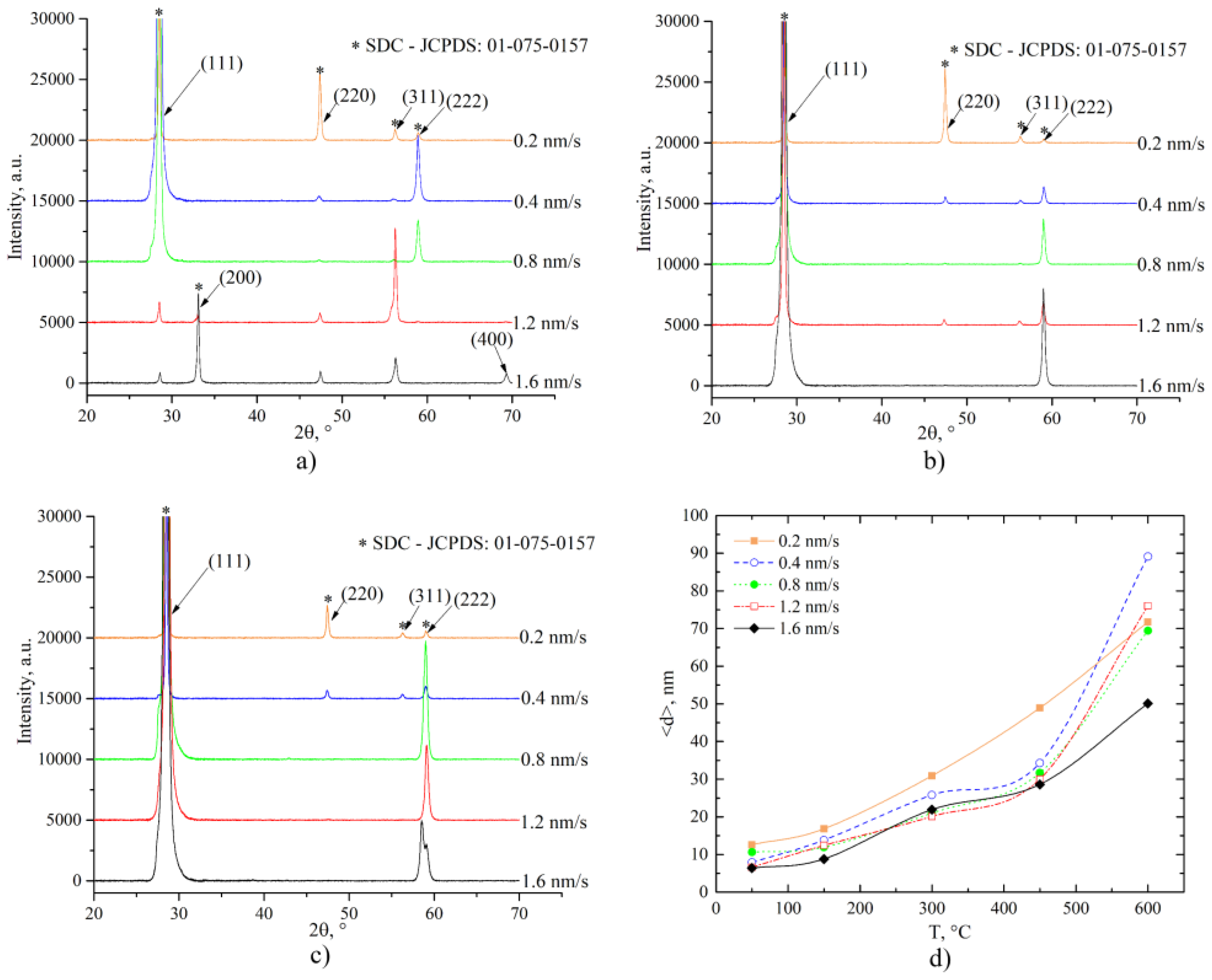
Patterns of SDC thin films (JCPSD No. 01-075-0157) have peaks belonging to (111), (200), (220), (311), (222), and (400) crystallographic orientations (Figure 1a–c). The positions of the peaks correspond to the fluorite structure, Fm3m space group. However, patterns of SDC thin films do not necessarily have all of these peaks. Peaks might disappear, or their intensities might change by changing the deposition parameters.
All SDC thin films deposited at 50 °C, 150 °C, and 300 °C temperature substrates have a similar structure. No influence of the specific surface area of powders was observed for the thin films deposited at the aforementioned temperatures. A different situation was observed when using 450 °C and higher temperature substrates during deposition. For example, SDC thin films deposited by evaporating powders of different surface areas on SiO2 substrates at 600 °C had a different crystalline structure (Figure 1a–c). X-ray diffraction patterns of SDC thin films deposited 6.2 m2/g by evaporating powder had peaks corresponding to (111), (200), (220), (311), (222), and (400) crystallographic orientations. The X-ray diffraction patterns of SDC thin films deposited by evaporating powder (11.3 m2/g) had peaks which corresponded to (111), (220), (311), and (222) crystallographic orientations. (200) and (400) crystallographic orientations disappeared. An arrangement of diffraction peaks in patterns of SDC thin films deposited by evaporating powder of 201.3 m2/g specific surface area, was very similar to the arrangement in patterns of SDC thin films deposited by evaporating powder of 11.3 m2/g specific surface area.
In addition, SDC thin films deposited by evaporating powders of 6.2 m2/g and 11.3 m2/g specific surface area changed their preferred orientation from (111) to (311), (200), and (220) (Figure 1a–c, Table 1). The preferred orientation changes to (311) and (200) orientation evaporating 6.2 m2/g of powder and using 1.2–1.6 nm/s deposition rates, respectively, and to (220) evaporating 11.3 m2/g of powder and using a 0.2 nm/s deposition rate. SDC thin films deposited by evaporating powder of 201.3 m2/g specific surface area did not change the preferred orientation.
The crystalline structure of thin SDC films depends on the composition of the vapor phase during the evaporation process. V. Piacente et. al. investigated the evaporation processes of the Ce-CeO2 mixture and CeO2 [21]. They found that the vapor phase consists of CeO2, CeO, and Ce where concentrations of CeO2 and Ce are 5 and 100 times lower, respectively than the concentration of CeO, if the mixture of Ce-CeO2 evaporates and the concentrations of CeO and Ce are four and six times lower, respectively than the concentrations of CeO2, if CeO2 evaporates. In addition, the reduction of CeO2 occurs on the surface (~7 nm) of CeO2 [22]. This means that the larger surface area of SDC powder is reduced if the powder of a larger specific surface area is used, i.e., there will be a deficiency of oxygen. The experiments of A.F. Orliukas et. al. proved this statement. They found that Ce3+ concentration is 14.16 % for powders of 8 m2/g specific surface area and 19.47 % for powders of 203 m2/g specific surface area [23]. Therefore, the concentration of CeO and Ce should increase and concentration of CeO2 should decrease in the vapor phase. This means that a higher number of CeO molecules and Ce atoms and lower number CeO2 molecules reach the surface of the substrate using powders with a large specific surface area. Moreover, the diffusion distance and time of CeO2 molecules is shorter than for CeO molecules and Ce adatoms [24]. As a result, the probability to form a crystallographic plane of higher surface energy (γ(111) < γ(200) < γ(220) < γ(311)) is higher when the concentration of CeO2 is higher in vapor flux. Adatoms do not have enough time to occupy the lowest energy state. Diffusion distance of adatoms and molecules increases in substrates of higher temperature. Hence, more surfaces of low surface energy ((111) and (222)) are formed. However, the probability to form surfaces of (111) and (222) may strongly decrease due to a strong decrease in surface energy at high temperatures. In this case, more surfaces of higher surface energy are formed, i.e., (200), (220), (311) or (400), meaning that the probability of changing preferred orientation increases.
Calculations of crystallite sizes revealed that the crystallite size of SDC thin films is higher for substrates of higher temperature (Figure 1d). The size of the crystallites changes from 6.40 nm to 89.1 nm. The reason is that the diffusion rate of adatoms is higher and the distance is longer for substrates at a higher temperature. Moreover, crystallites grow larger evaporating powders of a larger specific surface area (Table 2). An influence of the specific surface area of powders on the crystallite size was observed only for SDC thin films deposited at high temperatures (600 °C). Such changes in the crystallite size prove the statement that CeO and Ce concentrations are higher for powders with a larger specific surface area. The diffusion rates of CeO dissociation products and Ce adatoms are higher than the diffusion rates of CeO2 molecules or their dissociation products on the surface of the substrate.
3.2. Optical Band Gap Calculation
Ceria becomes conductive for oxygen ions when oxygen vacancies () are created by doping it with lower valence dopants (Sm, Gd) [1]. It is also known that ceria loses oxygen with decreasing partial pressure of oxygen and increasing temperature. This means that a reduction of Ce4+ to Ce3+ occurs, i.e., oxygen vacancies and electrons are created [2,22]. X-Ray photoelectron spectroscopy (XPS) measurements of SDC thin films deposited by evaporating powder of 6.2 m2/g specific surface areaproves the hypothesis about the reduction of Ce4+ to Ce3+. Concentration of Ce3+ varies from 24.5% to 29.1% [25].
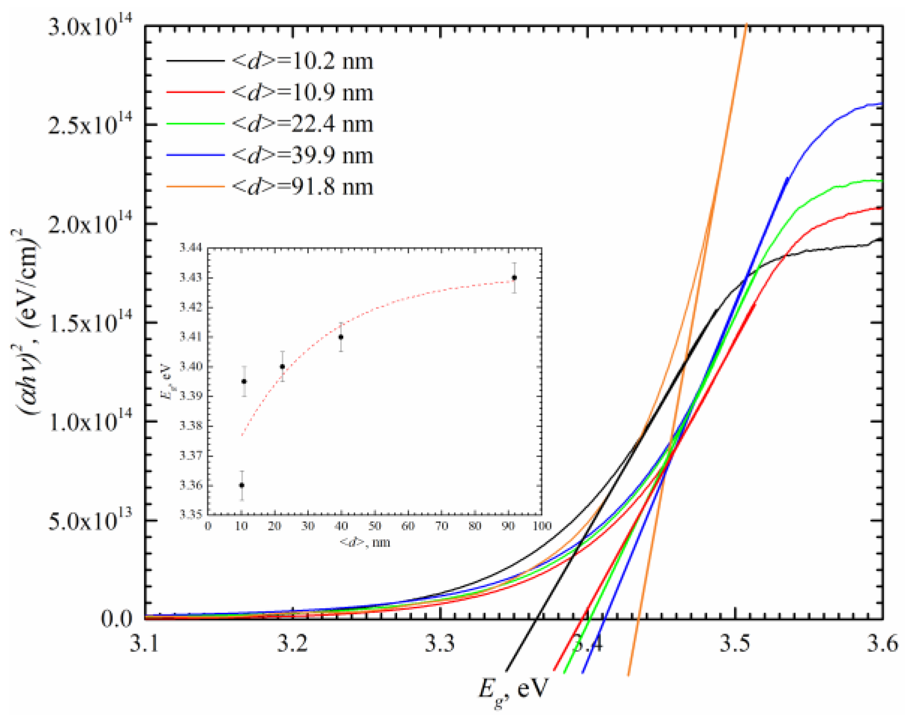
In addition, it was found that the optical band gap increases from 3.36 eV to 3.43 eV with increasing crystallite size from 10.2 nm to 91.8 nm (Figure 2). This means that the number of oxygen vacancies and the Ce3+ concentration decreases because the surface area where the reduction occurs also decreases with increasing crystallite size [26]. For this reason, fewer donor levels of Ce3+ are formed beneath the conduction band. Hence, SDC thin films are mixed ionic-electronic conductors.
3.3. SEM Results
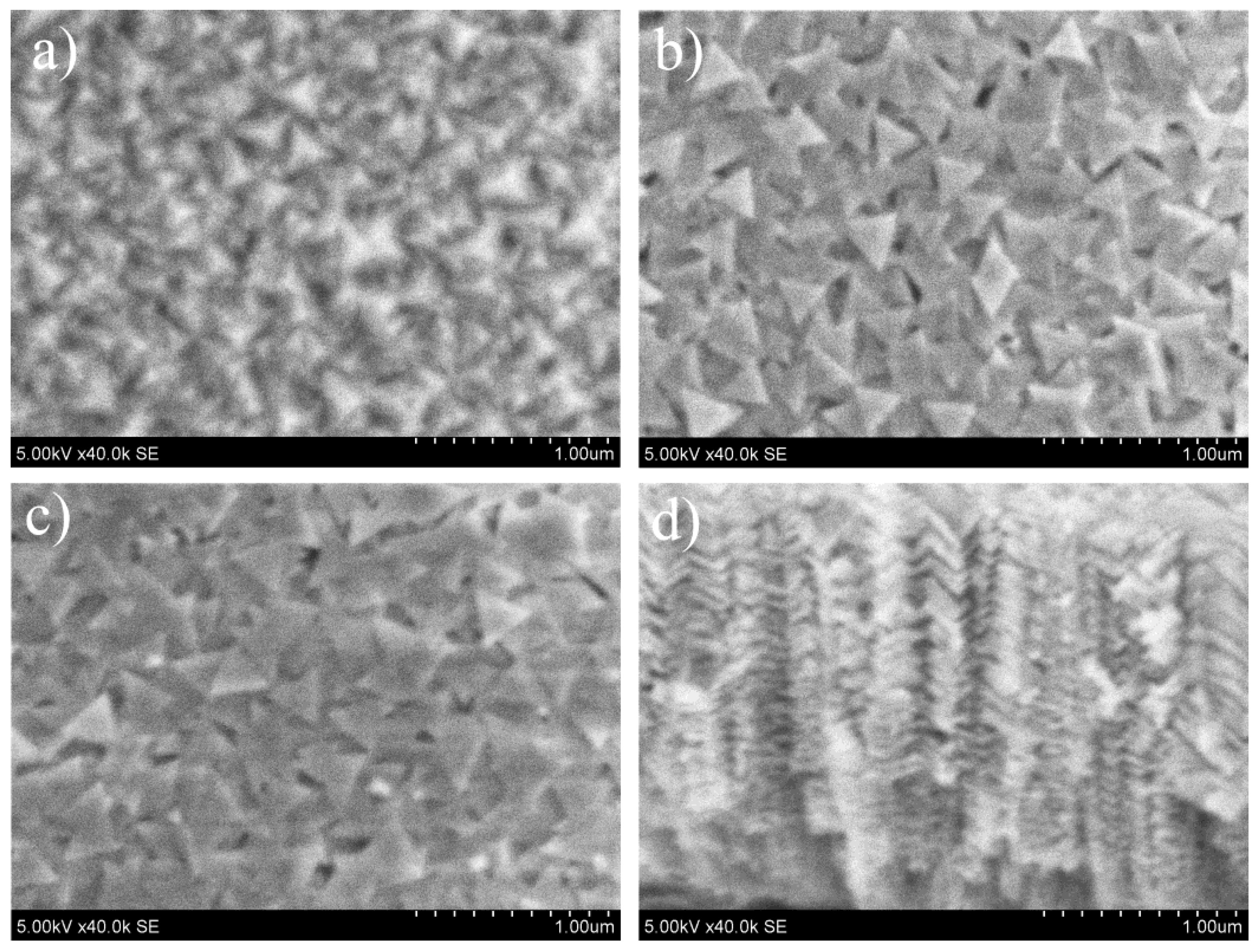
Thin films consist of grains with the shape of a triangular prism and growing on top of each other in the columnar way (Figure 3). The grain size increases with increasing temperature because the diffusion length of adatoms is longer for substrates of higher temperature. Hence, SDC thin films grow according to the structure zone models of Movchan–Demchishin and Grovenor in Zone 1 and Zone T [27,28]. Moreover, the surface morphology does not depend on substrate type (Figure 3b,c).
3.4. EIS Analysis
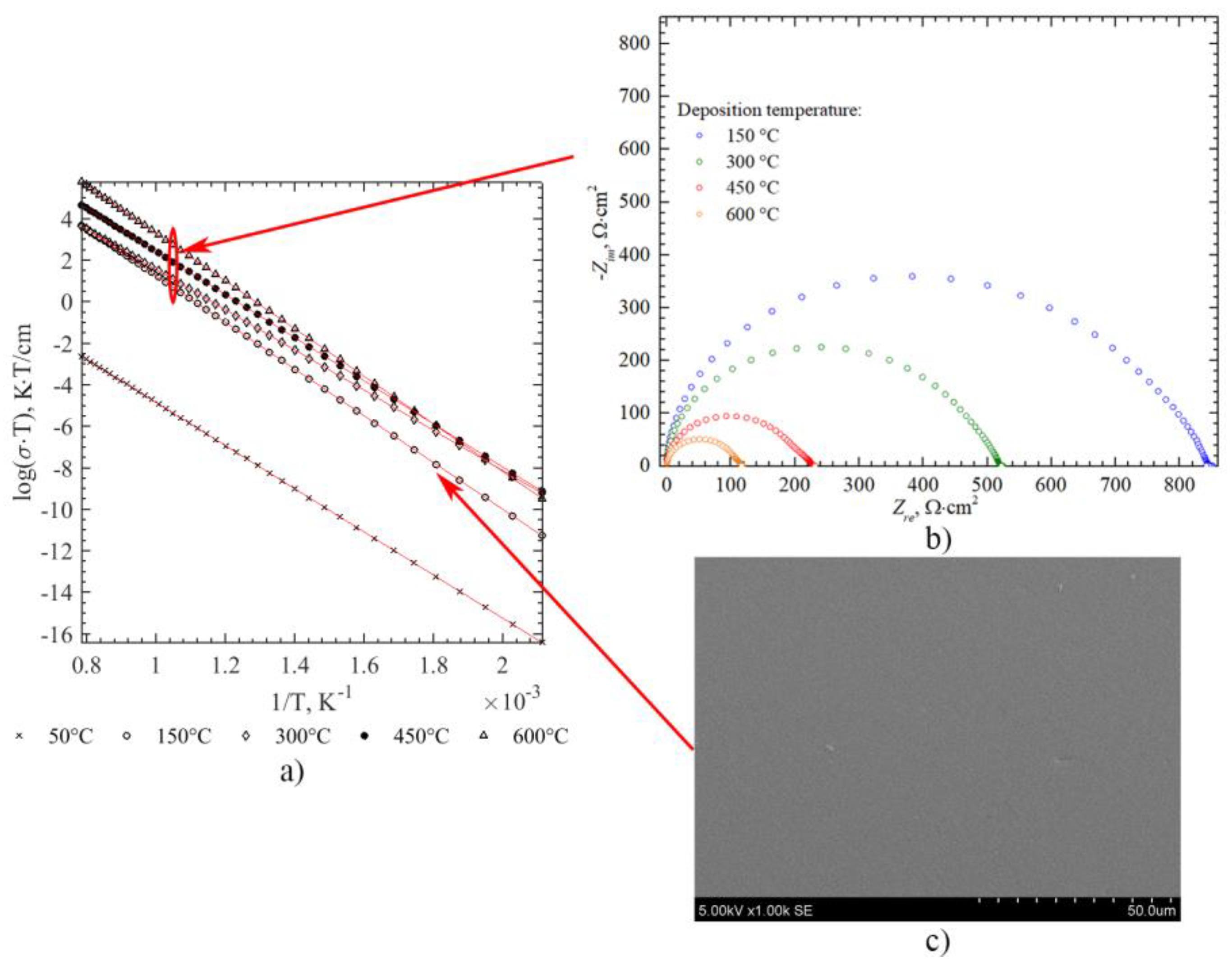
The activation energy of oxygen vacancies changed from 0.770 eV to 1.042 eV. No relationship between total conductivity and activation energy of oxygen vacancies was observed. In addition, no relationship between total conductivity and changes in preferred crystallographic orientation was determined. Quantitative calculations of total conductivity revealed that, for example, total conductivities of SDC thin films deposited by evaporating powder of 201.3 m2/g specific surface area on Al2O3 substrates using a 0.4 nm/s deposition rate are 4.4 × 10⁻⁷ S/cm, 9.0 × 10⁻⁴ S/cm, 1.5 × 10⁻³ S/cm, 3.3 × 10⁻³ S/cm, and 7.3 × 10⁻³ S/cm if 50 °C, 150 °C, 300 °C, 450 °C, and 600 °C substrates are used, respectively (Figure 4a). The values of the total conductivity were calculated for the experimental points measured at 600 °C. It follows that the total conductivity is higher if higher temperature substrates are used during deposition (Figure 4a). In addition, SDC thin films deposited on 50 °C substrates exhibit much lower total conductivity because some SDC thin films deposited on 50 °C–150 °C substrates are nonhomogeneous and have microcracks. These thin films have an extremely low total conductivity (3.4×10⁻⁸ S/cm–3.9×10−6 S/cm). In comparison, thin films deposited on higher temperature substrates are homogeneous (Figure 4c).
A semicircular shape (Figure 4b) indicates that there is more than one component of impedance in the Nyquist plot. However, the plots are very complex, and it is not possible to determine the number of components (RQ elements) and their contribution based on the Nyquist plot. Therefore, it was decided to use the distribution function of relaxation times (DFRT) in the impedance analysis.
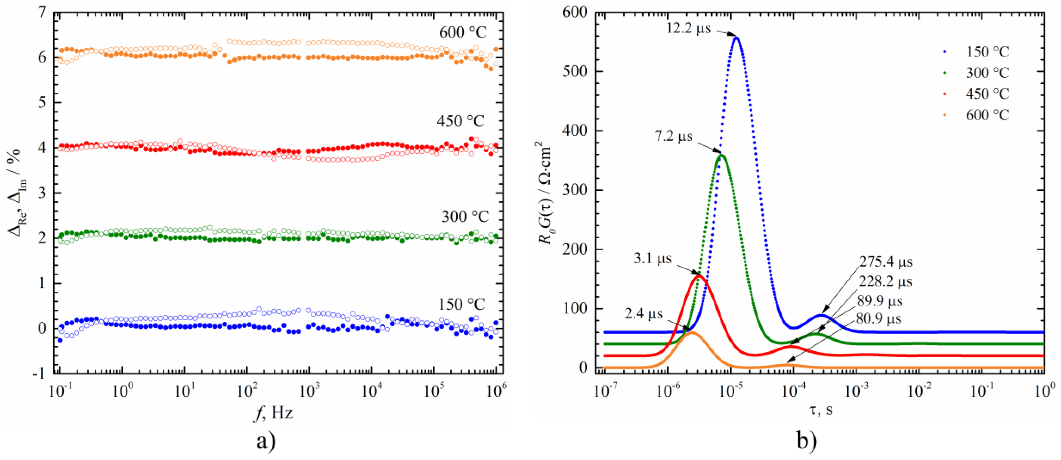
Firstly, the Kramers–Kronig (KK) transformations of real and imaginary parts were carried out to check the data validity. Calculations revealed that the relative residuals between the KK transformations and the experimental data are small (±0.25 %) (Figure 5a). Moreover, residuals do not show systematic deviations from abscissa axis. Therefore, the obtained results confirm the data validity and allow an analysis of the DFRT (Figure 5b). Two peaks are visible in the DFRT plots representing processes in “grains” and grain boundaries, respectively. The relaxation times from 2.4 µs to 12.2 µs represent processes in “gains” and the relaxation times from 80.9 µs to 275.4 µs represent processes in grain boundaries. A similar contribution was observed in all experiments.
According to Gobel M.C. et al., the increased ratio of grain boundary width (2b) to grain width (L) is the reason for the decrease in ionic conductivity because the grain boundaries have a blocking effect on the diffusion of oxygen ions [5]. The grain boundaries, which are parallel to the migration path of oxygen ions (perpendicular to the electrodes), affect the ionic conductivity [3]. However, it is not possible to decompose the measured impedance of “grain” into the impedance of the grain boundary and the grain because it is not possible to separate the impedance of circuit elements connected in parallel using EIS [29]. For these reasons, it is assumed that the short relaxation time component in the spectra of DFRT corresponds to the processes in the “grain”. The influence of grain boundaries on ionic conductivity (decrease) and electronic conductivity (increase) increase with a decreasing grain size. Moreover, it is reasonable to believe that the influence of substrate temperature and crystallite size on the conductivity of the SDC thin films is similar because the size of the crystallites is smaller when substrates of lower temperature are used during deposition (Figure 1d).
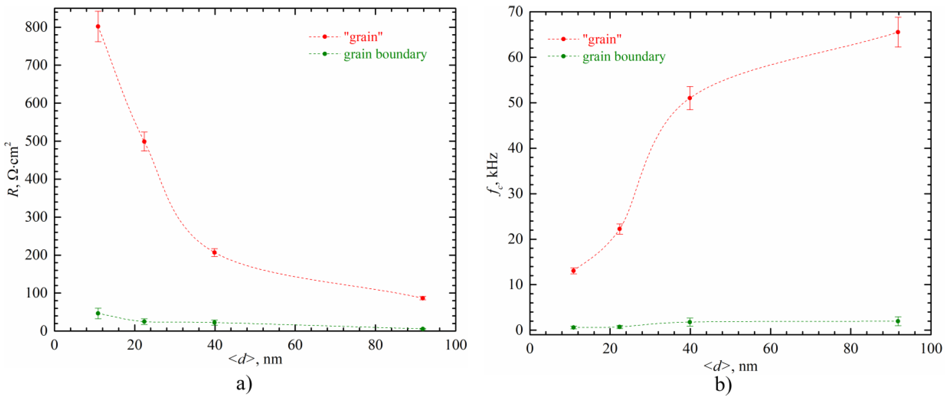
Indeed, calculations revealed that the normalized resistance of “grains” increases from 86.5 Ωcm2 to 802.1 Ωcm2 and the normalized resistance of grain boundaries increases from 5.8 Ωcm2 to 36.2 Ωcm2 when the crystallite size decreases from 91.8 nm to 10.9 nm (Figure 6a). Further, the resistance of “grains” is much higher than the resistance of grain boundaries (~18 times). The critical frequency of oxygen ions in “grains” increases from 13.1 kHz to 65.5 kHz and the critical frequency of oxygen ions in grain boundaries increases from 0.6 kHz to 2.0 kHz with increasing crystallite size from 10.9 nm to 91.8 nm (Figure 6b).
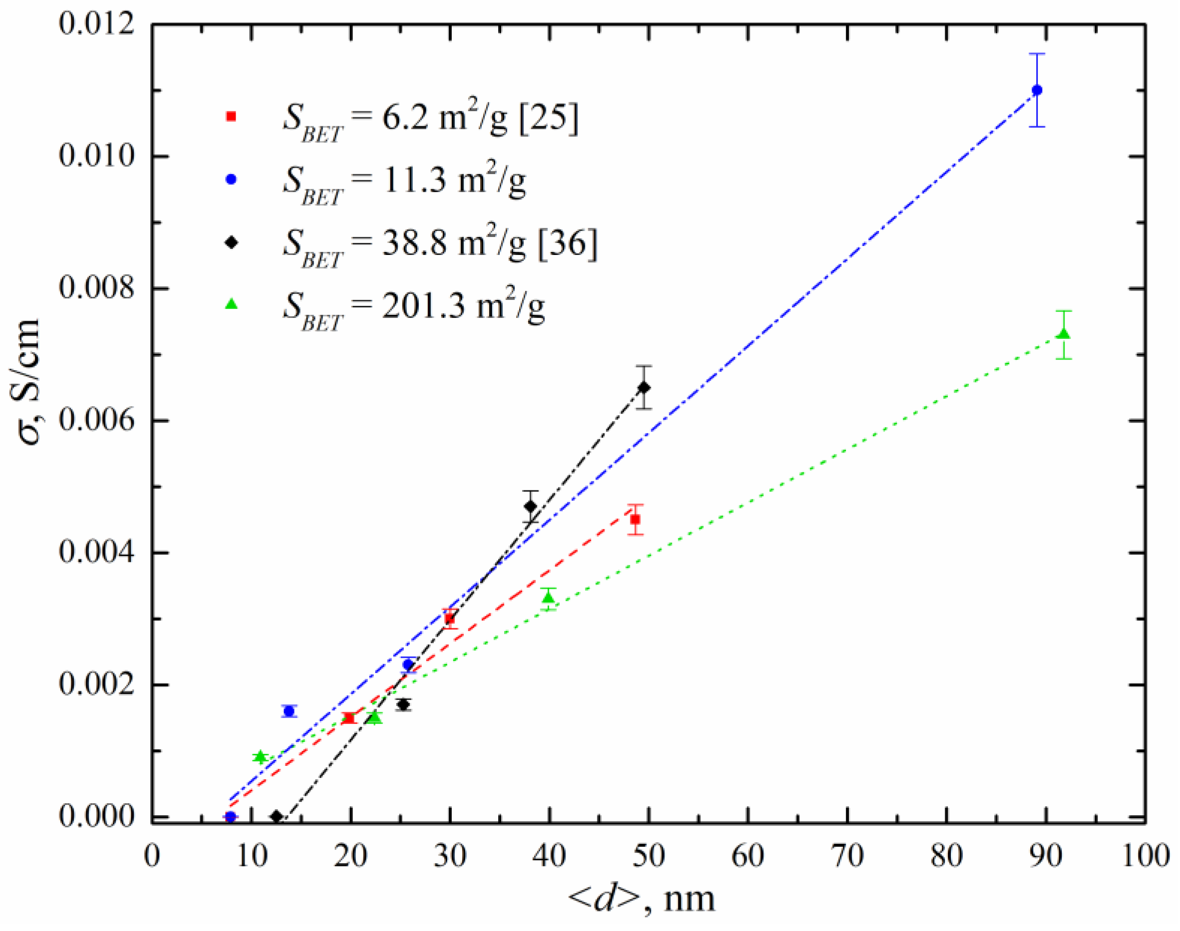
It follows that the total conductivity is higher if the SDC thin films have larger crystallites (Figure 7). The total conductivity is lower than 0.002 S/cm if the crystallite size is approximately 10–25 nm and more than 0.006 S/cm if the crystallite size is approximately 90 nm. The given values of ionic conductivity are calculated for impedance values measured at 600 °C. The highest value of total conductivity (1.1 × 10⁻² S/cm) is similar to the value obtained by other authors: 15SDC–0.013 S/cm [30]. Moreover, the total conductivity of SDC thin films is lower than Bi2V1,9Cu0,1O5,535 (3.3 × 10⁻¹ S/cm) and La0.85Sr0.15Ga0.2Mg0.2O2.825 (3.0 × 10⁻² S/cm), but higher than Yttrium-Stabilised Zirconia 8YSZ (6.4 × 10⁻³ S/cm), La1.8Gd0.2Mo2O9 (7.1 × 10⁻³ S/cm), La9.75Sr0.25Si6O26.875 (1.0 × 10⁻² S/cm) [30,31,32,33,34,35]. Such ionic conductivity is influenced by crystallite size, dopant concentration, and Ce3+ concentration. It is noteworthy that the ionic conductivity may vary greatly even if the thin films are formed with the same crystallite size (e.g., Figure 7, SBET = 11.3 m2/g and SBET = 201.3 m2/g). In most cases, this difference occurs due to morphological changes, e.g., increased porosity and different thin film growing kinetics. In the particular case presented in Figure 7, the difference in ionic conductivity appeared due to the lower density of the SDC thin films deposited using 201.3 m2/g powder.
4. Conclusions
An investigation of SDC thin films revealed that preferential crystallographic orientation (111) changes to (200), (220), (311) or (222) if 450–600 °C substrate temperatures and special deposition rates are used during deposition. It was also noticed that there is a relationship between changes in crystallographic orientation and specific surface area of initial powders. Preferential crystallographic orientation (111) tends to change its orientation to (200), (220) or (311) evaporating the powder of 6.2 m2/g specific surface area to (220) or (311) evaporating the powder of 11.3 m2/g specific surface area, and to (311) evaporating the powder of 201.3 m2/g specific surface area. Moreover, a smaller number of SDC thin films changed preferential crystallographic orientation for powders of higher specific surface areas. Crystallite size depended on the temperature of the substrate and specific surface area of the initial powder. Larger crystallites are obtained for substrates of higher temperature and larger specific surface area of powders. The size increases by 1.4 times if the powder of 6.2 m2/g specific surface area is changed to the powder of 201.3 m2/g specific surface area.
Changes in the microstructure can be explained by the changes in the gas phase composition. There was more CeO, Ce, and Sm and less CeO2 in the vapor phase when powders of the larger specific surface area were used. Hence, the diffusion distance and time of CeO and adatoms are longer.
It was noticed that the crystallite size has an impact on electrical properties of formed SDC thin films. The dependence of the optical band gap on the crystallite size proved that SDC thin films are mixed conductors and that the Ce3+ concentration decreases with increasing crystallite size. The total conductivity also increased with increasing crystallite size. The values of total conductivity are approximately 2.0 × 10⁻³ S/cm when the crystallite size is 10.0–25.0 nm and 6.0 × 10⁻³ S/cm when the crystallite size is 80.0 nm. The highest value of total conductivity was 1.1 × 10⁻² S/cm (600 °C) when crystallite sizes were 80.6 nm and 89.1 nm.
Author Contributions
Authors contributed equally to the manuscript. More specifically, conceptualization, M.S. and G.L.; methodology, K.B. and N.K.; formal analysis, M.S. and K.B.; investigation, M.S. and N.K.; writing—original draft preparation, M.S., K.B., G.L., and N.K.; writing—review and editing, M.S., K.B., G.L., and N.K.; validation, K.B. and N.K.; supervision, G.L.; funding acquisition, G.L.
Conflicts of Interest
The authors declare no conflict of interest.
References
- Tuller, H.L.; Bishop, S.R. Point Defects in Oxides: Tailoring Materials Through Defect Engineering. Annu. Rev. Mater. Res. 2011, 41, 369–398. [Google Scholar] [CrossRef]
- Migani, A.; Vayssilov, G.N.; Bromley, S.T.; Illas, F.; Neyman, K.M. Greatly facilitated oxygen vacancy formation in ceria nanocrystallites. Chem. Commun. 2010, 46, 5936–5938. [Google Scholar] [CrossRef] [PubMed]
- Tschöpe, A.; Sommer, E.; Birringer, R. Grain size-dependent electrical conductivity of polycrystalline cerium oxide: I. Experiments. Solid State Ionics 2001, 139, 255–265. [Google Scholar] [CrossRef]
- Daniele, P.; Vladimir, R.; Emiliana, F.; Christof, W.S.; Thomas, L.; Enrico, T.; John, A.K. Probing the bulk ionic conductivity by thin film hetero-epitaxial engineering. Sci. Technol. Adv. Mater. 2015, 16, 015001. [Google Scholar] [Green Version]
- Gobel, M.C.; Gregori, G.; Maier, J. Numerical calculations of space charge layer effects in nanocrystalline ceria. Part I: comparison with the analytical models and derivation of improved analytical solutions. Phys. Chem. Chem. Phys. 2014, 16, 10214–10231. [Google Scholar] [CrossRef] [PubMed]
- Gobel, M.C.; Gregori, G.; Maier, J. Numerical calculations of space charge layer effects in nanocrystalline ceria. Part II: detailed analysis of the space charge layer properties. Phys. Chem. Chem. Phys. 2014, 16, 10175–10186. [Google Scholar] [CrossRef] [PubMed]
- Gobel, M.C.; Gregori, G.; Maier, J. Mixed conductivity in nanocrystalline highly acceptor doped cerium oxide thin films under oxidizing conditions. Phys. Chem. Chem. Phys. 2011, 13, 10940–10945. [Google Scholar] [CrossRef] [PubMed]
- Tschöpe, A. Grain size-dependent electrical conductivity of polycrystalline cerium oxide II: Space charge model. Solid State Ionics 2001, 139, 267–280. [Google Scholar] [CrossRef]
- Bârcă, E.S.; Filipescu, M.; Luculescu, C.; Birjega, R.; Ion, V.; Dumitru, M.; Nistor, L.C.; Stanciu, G.; Abrudeanu, M.; Munteanu, C.; et al. Pyramidal growth of ceria nanostructures by pulsed laser deposition. Appl. Surf. Sci. 2016, 363, 245–251. [Google Scholar] [CrossRef]
- Balakrishnan, G.; Sundari, S.T.; Kuppusami, P.; Mohan, P.C.; Srinivasan, M.P.; Mohandas, E.; Ganesan, V.; Sastikumar, D. A study of microstructural and optical properties of nanocrystalline ceria thin films prepared by pulsed laser deposition. Thin Solid Films 2011, 519, 2520–2526. [Google Scholar] [CrossRef]
- Olding, T.; Sayer, M.; Barrow, D. Ceramic sol–gel composite coatings for electrical insulation. Thin Solid Films 2001, 398, 581–586. [Google Scholar] [CrossRef]
- Virbukas, D.; Laukaitis, G. The structural and electrical properties of samarium doped ceria films formed by e-beam deposition technique. Solid State Ionics 2017, 302, 107–112. [Google Scholar] [CrossRef]
- Laukaitis, G.; Virbukas, D. The structural and electrical properties of GDC10 thin films formed by e-beam technique. Solid State Ionics 2013, 247, 41–47. [Google Scholar] [CrossRef]
- Bail, A.L. Chapter 5 The Profile of a Bragg Reflection for Extracting Intensities. In Powder Diffraction: Theory and Practice; Dinnebier, R.E., Billinge, S.J.L., Eds.; The Royal Society of Chemistry: Cambridge, UK, 2008; pp. 134–165. [Google Scholar]
- Nagaraju, P.; Vijayakumar, Y.; Ramana Reddy, M.V. Optical and microstructural studies on laser ablated nanocrystalline CeO2 thin films. Glass Phys. Chem. 2015, 41, 484–488. [Google Scholar] [CrossRef]
- Boukamp, B.A. Linear Kronig-Kramers Transform Test for Immittance Data Validation. J. Electrochem. Soc. 1995, 142, 1885–1894. [Google Scholar] [CrossRef]
- Schönleber, M.; Klotz, D.; Ivers-Tiffée, E. A Method for Improving the Robustness of linear Kramers-Kronig Validity Tests. Electrochim. Acta 2014, 131, 20–27. [Google Scholar] [CrossRef]
- Schönleber, M.; Ivers-Tiffée, E. Approximability of impedance spectra by RC elements and implications for impedance analysis. Electrochem. Commun. 2015, 58, 15–19. [Google Scholar] [CrossRef]
- Tomoyasu, I.; Yasuhiro, Y.; Masataka, S. Electron-beam-assisted evaporation of epitaxial CeO2 thin films on Si substrates. J. Vac. Sci. Technol. A 2001, 19. [Google Scholar]
- Wan, T.H.; Saccoccio, M.; Chen, C.; Ciucci, F. Influence of the Discretization Methods on the Distribution of Relaxation Times Deconvolution: Implementing Radial Basis Functions with DRTtools. Electrochim. Acta 2015, 184, 483–499. [Google Scholar] [CrossRef]
- Piacente, V.; Bardi, G.; Malaspina, L.; Desideri, A. Dissociation energy of CeO2 and Ce2O2 molecules. J. Chem. Phys. 1973, 59, 31–36. [Google Scholar] [CrossRef]
- Kato, S.; Ammann, M.; Huthwelker, T.; Paun, C.; Lampimaki, M.; Lee, M.-T.; Rothensteiner, M.; van Bokhoven, J.A. Quantitative depth profiling of Ce3+ in Pt/CeO2 by in situ high-energy XPS in a hydrogen atmosphere. Phys. Chem. Chem. Phys. 2015, 17, 5078–5083. [Google Scholar] [CrossRef] [PubMed]
- Orliukas, A.F.; Šalkus, T.; Kežionis, A.; Venckutė, V.; Kazlauskienė, V.; Miškinis, J.; Laukaitis, G.; Dudonis, J. XPS and impedance spectroscopy of some oxygen vacancy conducting solid electrolyte ceramics. Solid State Ionics 2011, 188, 36–40. [Google Scholar] [CrossRef]
- Galdikas, A.; Čerapaitė-Truš, R.; Laukaitis, G.; Dudonis, J. Real-time kinetic modeling of YSZ thin film roughness deposited by e-beam evaporation technique. Appl. Surf. Sci. 2008, 255, 1929–1933. [Google Scholar] [CrossRef]
- Sriubas, M.; Pamakštys, K.; Laukaitis, G. Investigation of microstructure and electrical properties of Sm doped ceria thin films. Solid State Ionics 2017, 302, 165–172. [Google Scholar] [CrossRef]
- Dutta, P.; Pal, S.; Seehra, M.S.; Shi, Y.; Eyring, E.M.; Ernst, R.D. Concentration of Ce3+ and Oxygen Vacancies in Cerium Oxide Nanoparticles. Chem. Mater. 2006, 18, 5144–5146. [Google Scholar] [CrossRef]
- Movchan, B.A. Study of the Structure and Properties of Thick Vacuum Condensates of Nickel, Titanium, Tungsten, Aluminium Oxide and Zirconium Oxide. Fiz Met Metalloved. 1969, 28. [Google Scholar]
- Grovenor, C.R.M.; Hentzell, H.T.G.; Smith, D.A. The development of grain structure during growth of metallic films. Acta Metall. 1984, 32, 773–781. [Google Scholar] [CrossRef]
- Maier, J. On the Conductivity of Polycrystalline Materials. Berichte der Bunsengesellschaft für physikalische Chemie 1986, 90, 26–33. [Google Scholar] [CrossRef]
- Acharya, S.A.; Gaikwad, V.M.; D’Souza, S.W.; Barman, S.R. Gd/Sm dopant-modified oxidation state and defect generation in nano-ceria. Solid State Ionics 2014, 260, 21–29. [Google Scholar] [CrossRef]
- Kharton, V.V.; Marques, F.M.B.; Atkinson, A. Transport properties of solid oxide electrolyte ceramics: A brief review. Solid State Ionics 2004, 174, 135–149. [Google Scholar] [CrossRef]
- Guo, X.; Vasco, E.; Mi, S.; Szot, K.; Wachsman, E.; Waser, R. Ionic conduction in zirconia films of nanometer thickness. Acta Mater. 2005, 53, 5161–5166. [Google Scholar] [CrossRef]
- Wei, T.; Singh, P.; Gong, Y.; Goodenough, J.B.; Huang, Y.; Huang, K. Sr3-3xNa3xSi3O9-1.5x (x = 0.45) as a superior solid oxide-ion electrolyte for intermediate temperature-solid oxide fuel cells. Energy Environ. Sci. 2014, 7, 1680–1684. [Google Scholar] [CrossRef]
- Tsai, D.-S.; Hsieh, M.-J.; Tseng, J.-C.; Lee, H.-Y. Ionic conductivities and phase transitions of lanthanide rare-earth substituted La2Mo2O9. J. Eur. Ceram. Soc. 2005, 25, 481–487. [Google Scholar] [CrossRef]
- Belousov, V.V. Oxygen-permeable membrane materials based on solid or liquid Bi2O3. MRS Commun. 2013, 3, 225–233. [Google Scholar] [CrossRef]
- Sriubas, M.; Laukaitis, G. The influence of the technological parameters on the ionic conductivity of samarium doped ceria thin films. Mater. Sci. (Medžiagotyra) 2015, 21. [Google Scholar] [CrossRef]
Figure 1.
X-Ray Diffraction (XRD) measurements results: XRD patterns of thin Sm-doped cerium (SDC) films deposited on SiO2 substrate (600 °C) evaporating powders of (a) 6.2 m2/g, (b) 11.3 m2/g, (c) 201.3 m2/g specific surface area, and (d) dependences of crystallite size on SiO2 substrate temperature (11.3 m2/g powder).

Figure 2.
dependence on photon energy and band gap () dependence on crystallite size (〈〉).

Figure 3.
Topography (a, b, c) and cross section (d) images of thin SDC films deposited evaporating powder of 201.3 m2/g specific surface area with a 1.6 nm/s deposition rate. (a) 50 °C SiO2 substrate, (b) 600 °C SiO2 substrate, (c) 600 °C Al2O3 substrate, and (d) 600 °C SiO2 substrate.
Figure 3.
Topography (a, b, c) and cross section (d) images of thin SDC films deposited evaporating powder of 201.3 m2/g specific surface area with a 1.6 nm/s deposition rate. (a) 50 °C SiO2 substrate, (b) 600 °C SiO2 substrate, (c) 600 °C Al2O3 substrate, and (d) 600 °C SiO2 substrate.

Figure 4.
(a) Arrhenius plot and (b) Nyquist plots for SDC thin film deposited evaporating powder of 201.3 m2/g specific surface area on Al2O3 substrates with a 0.4 nm/s deposition rate and 150–600 °C substrate temperature, and (c) a topography image of a thin SDC film deposited on an Al2O3 substrate at 150 °C with a 0.4 nm/s deposition rate.

Figure 5.
(a) Relative residuals of the Kramers–Kronig (KK) test (closed symbols: Δre, open symbols: Δim. The data have been offset by steps of 2%) and (b) the DRFT’s plots for SDC thin films deposited by evaporating powder of 201.3 m2/g specific surface area and with a 0.4 nm/s deposition rate.
Figure 5.
(a) Relative residuals of the Kramers–Kronig (KK) test (closed symbols: Δre, open symbols: Δim. The data have been offset by steps of 2%) and (b) the DRFT’s plots for SDC thin films deposited by evaporating powder of 201.3 m2/g specific surface area and with a 0.4 nm/s deposition rate.

Figure 6.
(a) Dependencies of normalized resistance (R) on crystallite size and (b) Dependencies of critical frequency (fc) on crystallite size for SDC thin films deposited by evaporating powder of 201.3 m2/g specific surface area and with a 0.4 nm/s deposition rate.
Figure 6.
(a) Dependencies of normalized resistance (R) on crystallite size and (b) Dependencies of critical frequency (fc) on crystallite size for SDC thin films deposited by evaporating powder of 201.3 m2/g specific surface area and with a 0.4 nm/s deposition rate.

Figure 7.
Dependence of total conductivity () on crystallite size (〈〉) (0.4 nm/s deposition rate). Measurements were carried out on an Al2O3 substrates at 600 °C [25,36].


Table 1.
Texture coefficients of SDC thin films deposited by evaporating powders of different specific surface area on SiO2 substrates at 600 °C (vg—deposition rate).
Table 1.
Texture coefficients of SDC thin films deposited by evaporating powders of different specific surface area on SiO2 substrates at 600 °C (vg—deposition rate).
| SBET, m2/g | vg, nm/s | T(hkl)_SiO2 | |||||
|---|---|---|---|---|---|---|---|
| <111> | <200> | <220> | <311> | <222> | <400> | ||
| 6.2 | 1.2 | 0.2 | 0.3 | 0.2 | 3.2 | - | - |
| 6.2 | 1.6 | 0.1 | 3.0 | 0.3 | 0.8 | 1.5 | 0.1 |
| 11.3 | 0.2 | 1.3 | - | 1.7 | 0.2 | 0.7 | - |
Table 2.
Crystallite size (<d>SiO2) dependence on specific surface area of powders (SBET), 0.4 nm/s deposition rate, 600 °C temperature of SiO2 substrate.
Table 2.
Crystallite size (<d>SiO2) dependence on specific surface area of powders (SBET), 0.4 nm/s deposition rate, 600 °C temperature of SiO2 substrate.
| SBET, m2/g | 6.2 | 11.3 | 201.3 |
|---|---|---|---|
| <d>SiO2, nm | 66.5 ± 0.3 | 89.1 ± 0.6 | 91.8 ± 0.8 |
© 2018 by the authors. Licensee MDPI, Basel, Switzerland. This article is an open access article distributed under the terms and conditions of the Creative Commons Attribution (CC BY) license (http://creativecommons.org/licenses/by/4.0/).
Share and Cite
MDPI and ACS Style
Sriubas, M.; Bockute, K.; Kainbayev, N.; Laukaitis, G. Influence of the Initial Powder’s Specific Surface Area on the Properties of Sm-Doped Ceria Thin Films. Crystals 2018, 8, 443. https://0-doi-org.brum.beds.ac.uk/10.3390/cryst8120443
AMA Style
Sriubas M, Bockute K, Kainbayev N, Laukaitis G. Influence of the Initial Powder’s Specific Surface Area on the Properties of Sm-Doped Ceria Thin Films. Crystals. 2018; 8(12):443. https://0-doi-org.brum.beds.ac.uk/10.3390/cryst8120443
Chicago/Turabian StyleSriubas, Mantas, Kristina Bockute, Nursultan Kainbayev, and Giedrius Laukaitis. 2018. "Influence of the Initial Powder’s Specific Surface Area on the Properties of Sm-Doped Ceria Thin Films" Crystals 8, no. 12: 443. https://0-doi-org.brum.beds.ac.uk/10.3390/cryst8120443
Note that from the first issue of 2016, this journal uses article numbers instead of page numbers. See further details here.