Single Crystal Diamond Deposited by Dual Radio-Frequency Plasma Jet CVD with High Growth Rate


College of Materials Science and Opto-Electronic Technology, University of Chinese Academy of Sciences, Beijing 100049, China
*
Author to whom correspondence should be addressed.
Crystals 2019, 9(1), 32; https://0-doi-org.brum.beds.ac.uk/10.3390/cryst9010032
Submission received: 3 December 2018
/
Revised: 24 December 2018
/
Accepted: 6 January 2019
/
Published: 10 January 2019
(This article belongs to the Special Issue Synthesis and Characterization of Diamond Crystals)
Abstract
:Single crystal diamonds were deposited on high pressure high temperature (HPHT) substrate with high growth rate, up to 18.5 μm/h, by using dual radio-frequency inductive coupled plasma jet. The methane flux was found to influence the growth rate of single crystal diamond. The reason for this might be ascribed to the electron temperature increase, raising the flux of methane, based on the plasma diagnosis results by optical emission spectra (OES). The results of Raman spectroscopy and the X-ray rocking-curve indicated that as-deposited diamonds are of good quality.
1. Introduction
Diamonds have a large range of potential applications [1,2,3,4,5]. Due to their high atomic density, strong bonding, and crystal structure of high symmetry, diamonds show high Raman gain coefficient, which makes them suitable for high power diamond Raman lasers [6]. With a wide bandgap of 5.5 eV, a high breakdown field, high carrier mobility, and high radiation hardness, diamonds are an ideal material for high energy particle and ionizing radiation detection [7,8,9,10]. Furthermore, diamonds exhibit exceptional electronic properties, such as a high breakdown field (>10 MV/cm) and high carrier mobility (4500 cm2/Vs for electrons and 3800 cm2/V for holes), which makes diamond an excellent candidate for next generation semiconductor materials [11,12].
Due to the fact that high energy plasma can dissociate reaction gas very effectively and can provide high atomic hydrogen concentration, which is necessary for fabricating high-quality, large area single crystal diamond (SCD), plasma enhanced chemical vapor deposition (PECVD) has been widely used for SCD growth [13]. According to plasma sources, PECVDs can be classified as microwave-, direct current (DC)-, and radio frequency (RF) plasma CVD. Among all these methods, microwave plasma CVD is the most widely used method, the reported largest area reached 2 inches in diameter, and the fastest growth rate reached 105 μm/h [14,15,16,17].
Like microwave plasma, RF plasma is free from metal electrode contamination. However, RF plasma possess longer wavelengths, so that electrons and positive charged particles in the plasma can get energy from the whole electromagnetic wave vibration period, which leads to more uniform spatial distribution [18]. According to previous reports, plasma density higher than 1018 m−3 can be achieved by radio frequency inductively coupled plasma (RF-ICP). Since the 1980s, researchers have been growing diamond films by RF CVD, and the reported diamond films can be deposited uniformly on a substrate as large as 100 mm in diameter, and the growth rate can reach 30 μm/h [19,20]. At the beginning of the 21st century, the growth rate reached 70 μm/h [21]. However, some drawbacks exist in the RF plasma CVD growth method, such as “hollow shaped” plasma found in the annular discharge zone caused by skin effect easily, which results in a non-diamond composition, and “ion bombardment” caused by plasma self-bias voltage, which damages diamond growth [22,23]. According to our past research, dual RF-ICP can be considered as an effective way to avoid these problems. Moreover, poly-crystal and single-crystal diamond films have been fabricated successfully by very low growth rates [24,25,26,27]. In this work, by adjusting growth condition, the growth rate of the SCD films have been greatly enhanced, and the maximum growth rate can exceed 18 μm/h.
2. Materials and Methods
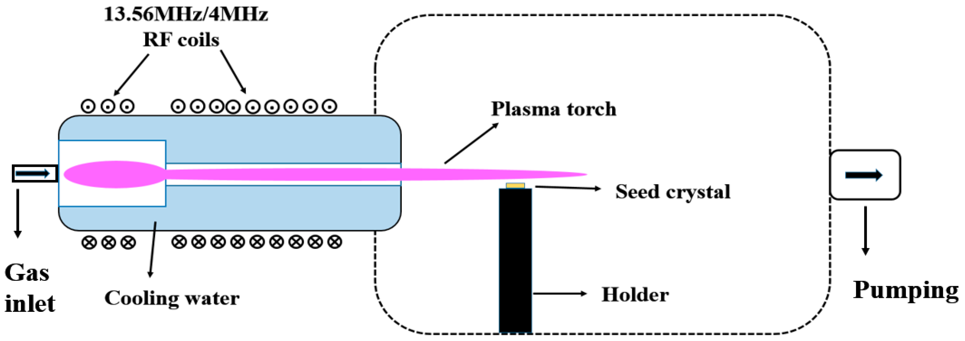
Single crystal HPHT Ιb (100) diamonds (5 mm × 5 mm and 6 mm × 6 mm) were used as seed substrates. A diagram of the dual RF-ICP jet CVD system used in this work is shown in Figure 1, in which commercial 13.56 MHz and 4 MHz RF power coils were tandemly set on the plasma generator. The high frequency coils were used to excite plasma, and the low frequency coils were used to increase plasma energy. Based on this arrangement, the plasma generator, as well as the reactive gas inlet, were further optimized to increase the SCD deposition rate. A mixture of Ar\H2\CH4 was used as working feed gas with flow rate controlled by the mass-flow controllers. Before deposition process, the substrate was heated to 300 °C in an acid mixture (H2SO4:HNO3 = 5:1) for 30 min, followed by ultrasonic clean up under acetone, ethanol, and deionized water to remove excess solvent residues. Detailed deposition parameters are listed in Table 1.
The gas phase species in dual-RF plasma WERE diagnosed by optical emission spectra (OES) (sofn instruments, Beijing, China). The deposited SCDs were characterized by X-ray diffraction (XRD) (Rigaku Ultima IV, Tokyo, Japan), field emission scanning electron microscopy (SEM) (KYKY Technology, Beijing, China) and Raman spectroscopy (Renishaw, London, England).
3. Results and Discussion
3.1. Plasma Diagnosed by Optical Emission Spectra (OES)
OES was applied to diagnose the dual-RF plasma, with the working feed gas of Ar/H2/CH4. OES of plasma was collected through a quartz window under the same instrument parameter setting. The scan range was from 400 nm to 700 nm with a 0.2 nm scanning step.
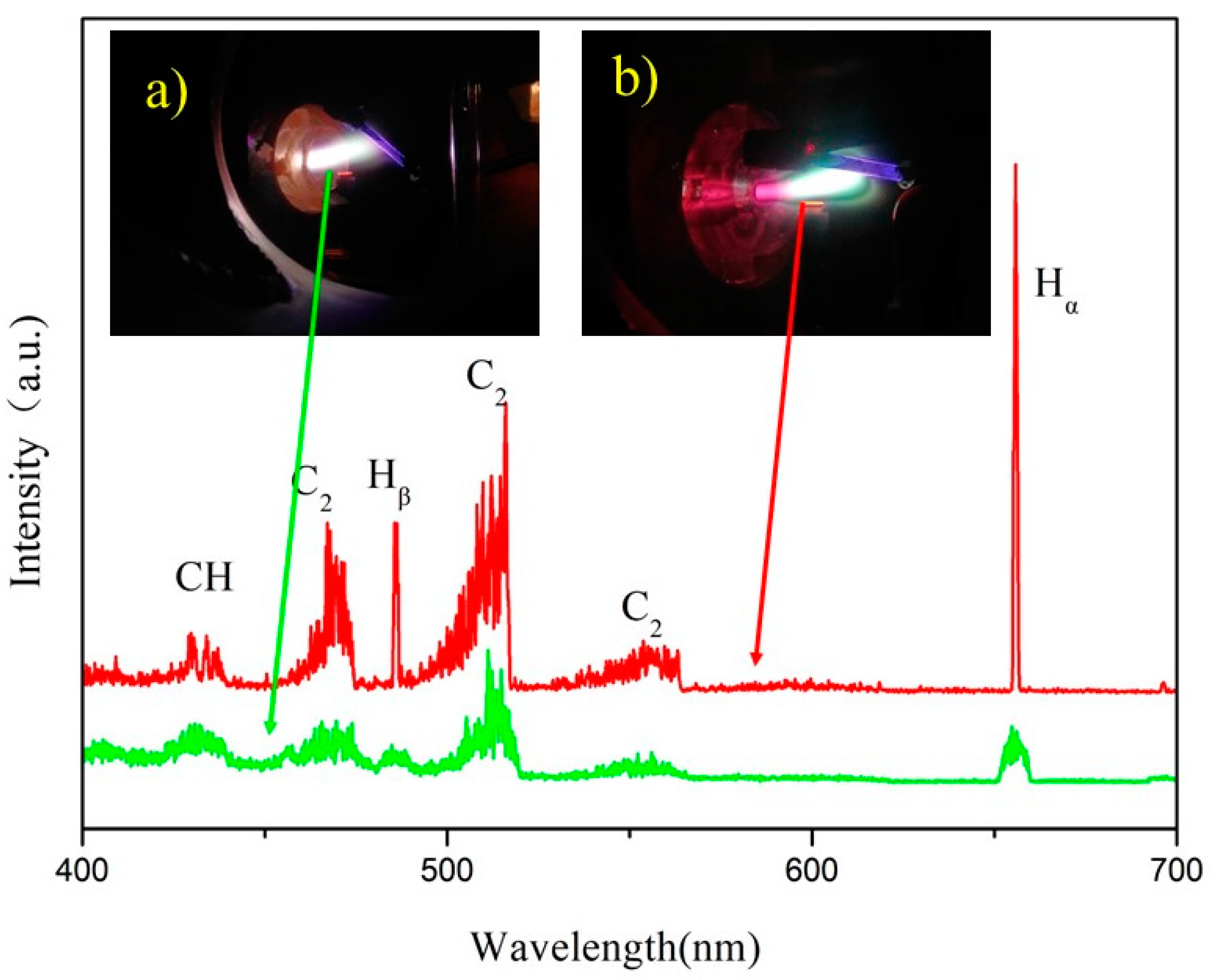
Two introduction methods of feed gas were compared. One was the regular feed gas introduction method, which was used to introduce the mixture of CH4/H2/Ar to pass through the RF electromagnetic field. The other method was the modified method which was used to introduce the mixture of H2/Ar to pass through the RF electromagnetic field, form high density H2/Ar plasma beam, and introduce the CH4 downstream of the H2/Ar. This means that the methane was dissociated by H2/Ar plasma rather than the RF electromagnetic. Figure 2 is the OES result under the different feed gas introduction methods. The insets are the images of the corresponding plasma. The observed emission peaks correspond to C2 (471 nm, 516.1 nm, 561 nm swan bands), Hα (656.1 nm), Hβ (486.1 nm) and CH (388.9 nm and 431.5 nm) for both gas introduction methods, which is a typical spectrum for diamond deposition, just like that of microwave plasma and DC-arc plasma [28,29]. However, the intensity of C2 and Hα were higher in the modified method than those in the regular method, which means that the concentration of the H-related radicals and the C-related radicals were higher in case of modified feed gas introduction method. From the insets, it can be seen that the plasma volume in the modified method was larger than that in the regular method, which is suitable for large area diamond deposition. As the quality and growth rate of the deposited diamond films depend on active radical densities on the substrate surface, the modified feed gas introduction method was adopted in the following deposition procedures.
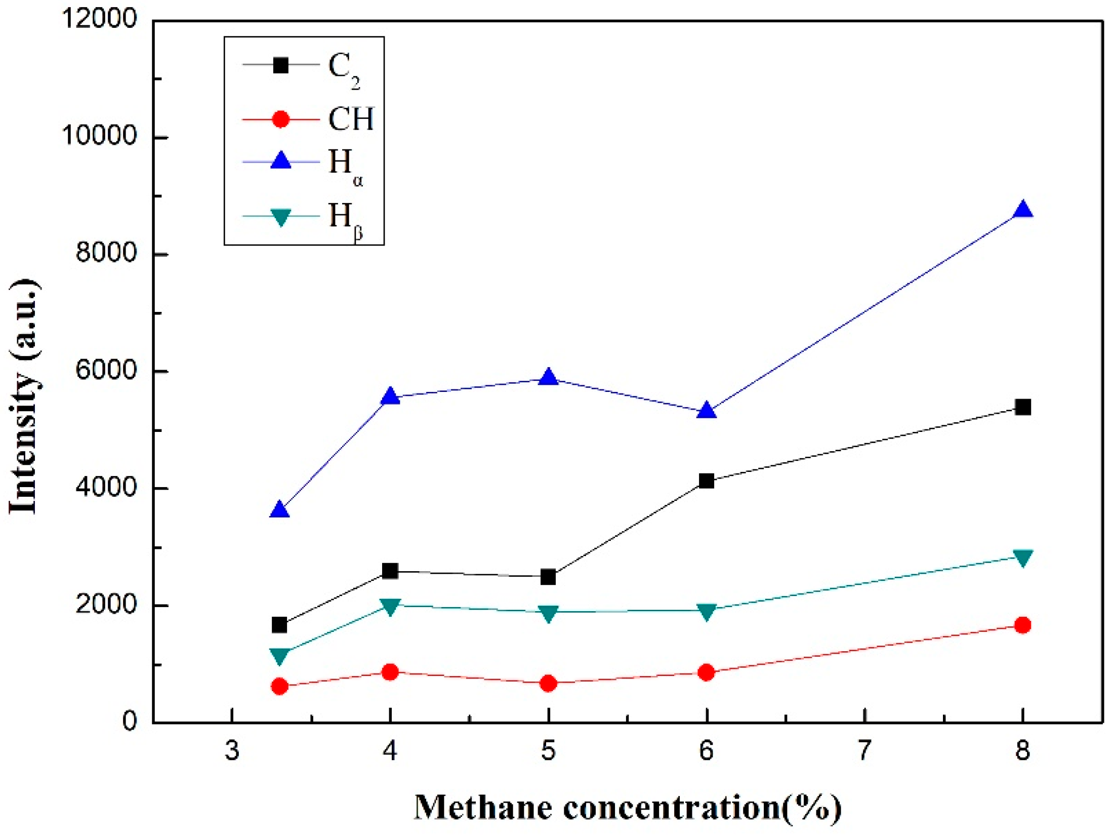
Figure 3 shows the OES results of the dual-RF plasma. With the methane concentration varying from 3.3% to 8%, the intensity of the C2 (516.1 nm), Hα (656.1 nm), Hβ (486.1 nm), CH (431.5 nm) under different CH4 concentration is plotted in Figure 3. As shown in Figure 3, a slight increase of CH4 concentration led to a strong increase of both C and H related radicals. This phenomenon is due to the CH4 dissociation reaction. The change of Hα, Hβ, and CH intensity was negligible when CH4 concentration increased from 4% to 6%, however, there was a noticeable increase when CH4 concentration was higher than 6%. C2 intensity showed a rapid growth when CH4 concentration reached 5%. The condition of the plasma can be deduced from the ratio between Hβ and Hα. Compared to our previous work [27], the electron temperature (Te) of the plasma was increased from 2.48 eV to 3.92 eV, indicating a strong enhancement of the plasma energy.
3.2. Characterization of Diamond Films
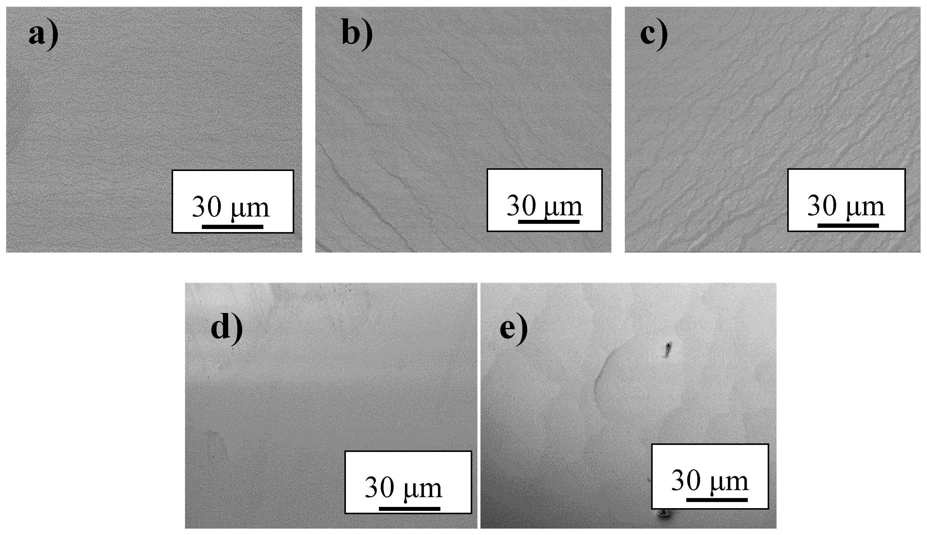
Figure 4 shows the effect of methane concentration on the surface morphology of the deposited diamond films. With the increase of methane concentration, the morphology of the as-grown diamond film changed from stepped growth mechanism to overlapping “hills”, which means that the growth mode changed from 2D layer growth to 3D island growth [30]. From Figure 4a–c, we can see that the diamond film surface was covered by step flows, and with the increase of methane concentration the steps become denser and more disordered. When the methane concentration reached 6%, smooth growth surface was achieved. With further increases of methane concentration, overlapping “hills” can be observed, the growth mechanism changed to island growth, which means that the crystal quality was decreased [31].
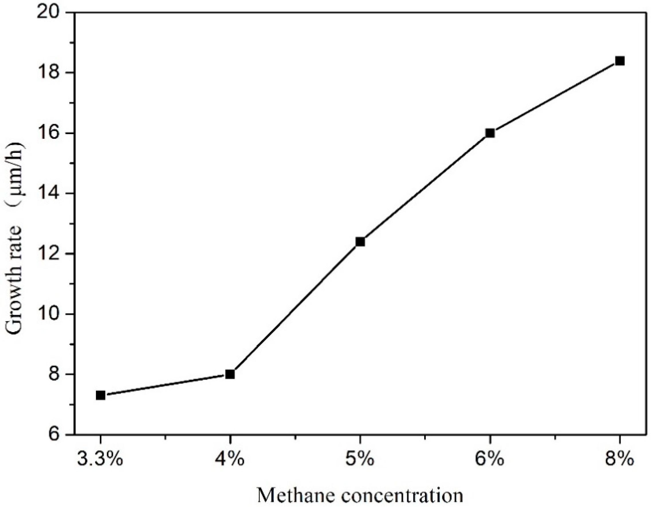
The film deposition rate with different methane concentration is plotted in Figure 5. The deposition rate increased rapidly with the increase of methane concentration. After 10 h deposition, the thickness of the samples increased by 73 μm, 80 μm, 125 μm, 161 μm, and 185 μm, respectively.
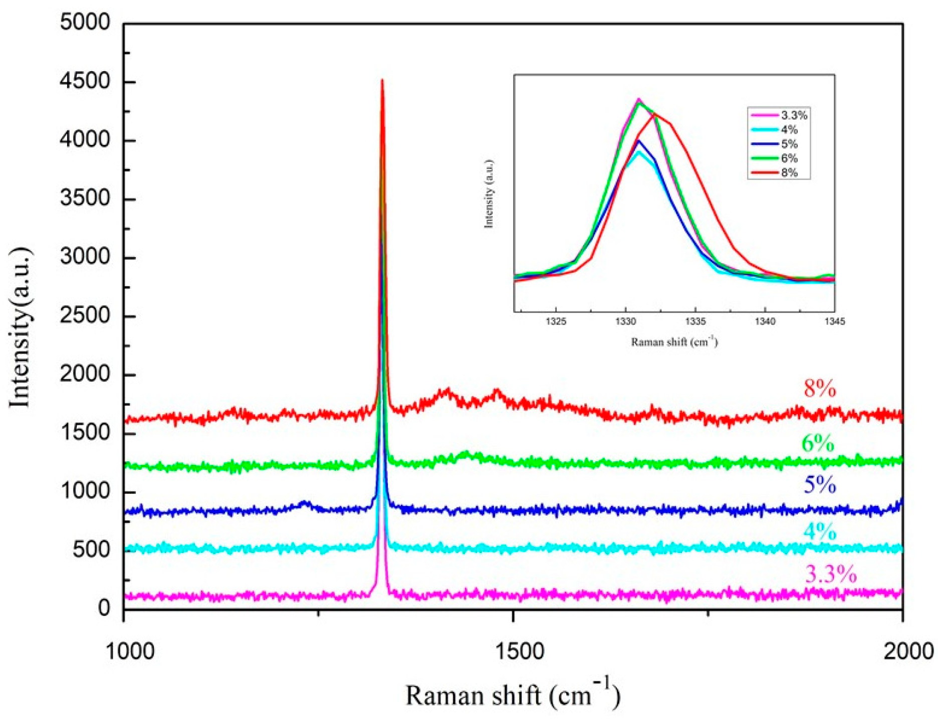
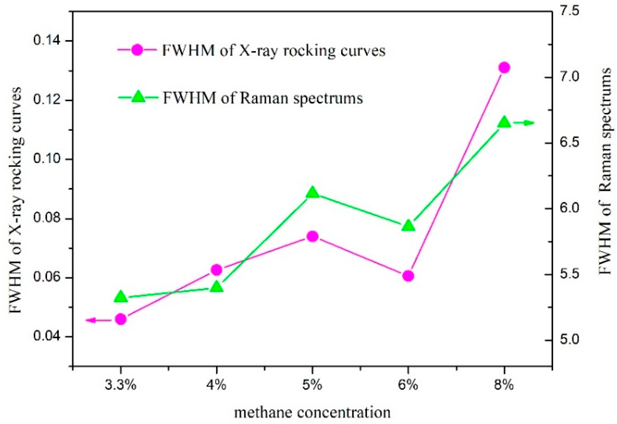
Figure 6 shows the Raman spectra of the diamond films. When methane concentration increased from 3.3% to 8%, the diamond peaks were 1330.8 cm−1, 1330.9 cm−1, 1330.9 cm−1, 1330.9 cm−1 and 1332.1 cm−1, respectively. The position of the diamond peak shows obvious negative shift, indicating a certain amount of tensile stress existed inside the films. According to Boppart’s study [32], we can figure out that the specific value of tensile stress was 0.592 GPa, 0.557 GPa, 0.557 GPa, 0.557 GPa and 0.139 GPa, respectively. The tensile stress in the diamond films decreased quickly when methane concentration was higher than 6%. Compared with the surface morphology, when the methane concentration reached 6%, the growth mechanism changed from 2D layer growth to 3D island growth. We guess that the change of growth mechanism led to the reduction of stress in the crystals. From the Raman spectra, we can see that, when the methane concentration was higher than 6%, the scattering broadband among 1350.0–1600.0 cm−1 was observed, which came from the sp2 C–C bond. Figure 7 shows the full wave at half maximum (FWHMs) of X-ray rocking curves and Raman spectrums of the deposited diamond films with methane concentration varying from 3.3% to 8%. When the concentration of methane increased, the quality of the SCD films displayed a decreased trend.
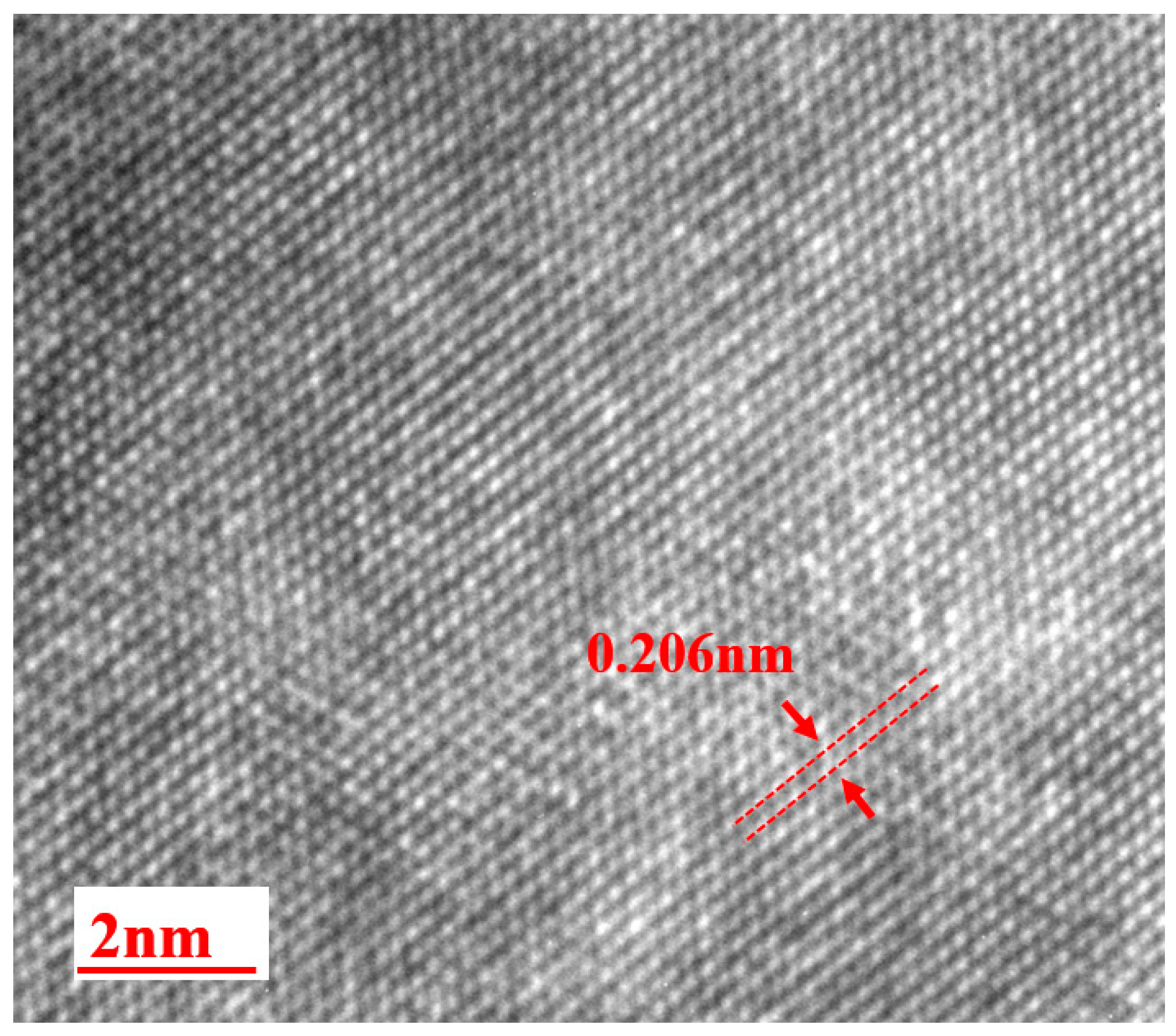
When the methane concentration reached 6%, the deposited films showed a relatively high growth rate and good crystal quality. We tried a 50 h deposition at two 6 × 6 mm2 HPHT seeds at the same time. The fourier transform infrared spectroscopy (FTIR) of the detached grown layer and HPHT diamond substrate are shown in Figure 8. The inset is the image of the grown diamond. The transmission coefficient of the deposited film was better than the HPHT diamond substrate. At 1130 cm−1, 1282 cm−1, and 1344 cm−1, deposited diamond film showed lower absorption coefficient, indicating lower nitrogen impurity. The strong bands at 1900 to 2300 cm−1 were the inherent two phonon lines of diamond associated with C–C bonds and were present in both deposited diamond films and HPHT substrates [33]. Figure 9 is the high resolution transmission electron microscopy (HRTEM) micrograph of the deposited single crystal diamond and d-spacing of the deposited diamond was measured to be 0.206 nm, coinciding with that of the diamond (111) plane. There were no defects observed, like dislocations and stacking faults, in the detected zone.
4. Conclusions
In this article, we investigated single-crystal diamond growth by dual RF-plasma jet CVD. Methane concentration strongly influenced the concentrations of CH, C2, Hβ, Hα, and their proportions in the gas phase, especially C2. The morphology of the as-grown diamond film changed from step flows to islands, which means that the growth mode changed from 2D layer growth to 3D island growth. The SCD films were rapidly deposited by dual RF CVD, and the growth rate increased with methane concentration. To our knowledge, this was the first time the fast deposition of single crystal diamond by RF plasma CVD has been realized.
Author Contributions
Conceptualization, G.-c.C. and H.L.; methodology, H.L. and J.-j.L.; software, Z.-r.L. and K.X.; validation, H.L., Z.-r.L. and K.X.; formal analysis, H.L.; investigation, Z.-j.C.; resources, Z.-j.C.; data curation, H.L.; writing—original draft preparation, H.L.; writing—review and editing, G.-c.C. and H.L.; supervision, G.-c.C.; project administration, G.-c.C.; funding acquisition, G.-c.C.
Funding
This work is supported by National Natural Science Foundation of China (50128790), Hundred program of Chinese Academy of Sciences, Hundred Talents Program of the Chinese Academy of Sciences, Scientific Research Equipment Project of the Chinese Academy of Sciences (yz201356), Hebei Science and Technology Plan (14291110D), Beijing Science and Technology Project (Z151100003315024).
Conflicts of Interest
The authors declare no conflict of interest.
References
- May, P.W. The new diamond age. Science 2008, 320, 1490–1491. [Google Scholar] [CrossRef]
- Isberg, J.; Hammersberg, J.; Johansson, E.; Wikström, T.; Twitchen, D.J.; Whitehead, A.J.; Coe, S.E.; Scarsbrook, G.A. High carrier mobility in single-crystal plasma-deposited diamond. Science 2002, 297, 1670–1672. [Google Scholar] [CrossRef]
- May, P.W. Diamond thin films: A 21st-century material. Philos. Trans. R. Soc. Lond. A Math. Phys. Eng. Sci. 2000, 358, 473–495. [Google Scholar] [CrossRef]
- Isberg, J.; Hammersberg, J.; Twitchen, D.J.; Whitehead, A.J. Single crystal diamond for electronic applications. Diamond Relat. Mater. 2004, 13, 320–324. [Google Scholar] [CrossRef]
- Aharonovich, I.; Castelletto, S.; Simpson, D.A.; Su, C.H.; Greentree, A.D.; Prawer, S. Diamond-based single-photon emitters. Rep. Prog. Phys. 2011, 74, 076501. [Google Scholar] [CrossRef]
- Williams, R.J.; Kitzler, O.; Bai, Z.; Sarang, S.; Jasbeer, H.; McKay, A.; Mildren, R.P. High Power Diamond Raman Lasers. IEEE J. Sel. Top. Quantum Electron. 2018, 24, 1–14. [Google Scholar] [CrossRef]
- Obraztsova, O.; Ottaviani, L.; Klix, A.; Döring, T.; Palais, O.; Lyoussi, A. Comparing the Response of a SiC and a sCVD Diamond Detectors to 14-MeV Neutron Radiation. IEEE Trans. Nucl. Sci. 2018, 65, 2380–2384. [Google Scholar] [CrossRef]
- Kumar, A.; Topkar, A. A Study of the Fast Neutron Response of a Single-Crystal Diamond Detector at High Temperatures. IEEE Trans. Nuclear Sci. 2018, 65, 630–635. [Google Scholar] [CrossRef]
- Girolami, M.; Bellucci, A.; Calvani, P.; Trucchi, D.M. Large single-crystal diamond substrates for ionizing radiation detection. Phys. Status Solidi A 2016, 213, 2634–2640. [Google Scholar] [CrossRef]
- Schirru, F.; Kisielewicz, K.; Nowak, T.; Marczewska, B. Single crystal diamond detector for radiotherapy. J. Phys. D Appl. Phys. 2010, 43, 265101. [Google Scholar] [CrossRef] [Green Version]
- Umezawa, H. Recent advances in diamond power semiconductor devices. Mater. Sci. Semicond. Process. 2018, 78, 147–156. [Google Scholar] [CrossRef]
- Yamaguchi, H.; Masuzawa, T.; Nozue, S.; Kudo, Y.; Saito, I.; Koe, J.; Okano, K. Electron emission from conduction band of diamond with negative electron affinity. Phys. Rev. B 2009, 80, 165321. [Google Scholar] [CrossRef] [Green Version]
- Silva, F.; Achard, J.; Brinza, O.; Bonnin, X.; Hassouni, K.; Anthonis, A.; Barjon, J. High quality, large surface area, homoepitaxial MPACVD diamond growth. Diamond Relat. Mater. 2009, 18, 683–697. [Google Scholar] [CrossRef]
- Ralchenko, V.G.; Smolin, A.A.; Konov, V.I.; Sergeichev, K.F.; Sychov, I.A.; Vlasov, I.I.; Khomich, A.V. Large-area diamond deposition by microwave plasma. Diamond Relat. Mater. 1997, 6, 417–421. [Google Scholar] [CrossRef]
- Silva, F.; Hassouni, K.; Bonnin, X.; Gicquel, A. Microwave engineering of plasma-assisted CVD reactors for diamond deposition. J. Phys. Condens. Matter 2009, 21, 364202. [Google Scholar] [CrossRef]
- Yamada, H.; Chayahara, A.; Ohmagari, S.; Mokuno, Y. Factors to control uniformity of single crystal diamond growth by using microwave plasma CVD. Diamond Relat. Mater. 2016, 63, 17–20. [Google Scholar] [CrossRef]
- Li, F.; Zhang, J.; Wang, X.; Zhang, M.H.; Wang, H.X. Fabrication of Low Dislocation Density, Single-Crystalline Diamond via Two-Step Epitaxial Lateral Overgrowth. Crystals 2017, 7, 114. [Google Scholar] [CrossRef]
- Kim, Y.D.; Lee, H.C.; Chung, C.W. A study on the maximum power transfer condition in an inductively coupled plasma using transformer circuit model. Phys. Plasmas 2013, 20, 093508. [Google Scholar] [CrossRef]
- Matsumoto, S.; Hino, M.; Kobayashi, T. Synthesis of diamond films in a rf induction thermal plasma. Appl. Phys. Lett. 1987, 51, 737–739. [Google Scholar] [CrossRef]
- Kohzaki, M.; Uchida, K.; Higuchi, K.; Noda, S. Large-area high-speed diamond deposition by RF induction thermal plasma chemical vapor deposition method. Jpn. J. Appl. Phys. 1993, 32, L438. [Google Scholar] [CrossRef]
- Berghaus, J.O.; Meunier, J.L.; François, G. Direct current bias effects in RF induction thermal plasma diamond CVD. IEEE Trans. Plasma Sci. 2002, 30, 442–449. [Google Scholar] [CrossRef]
- Greenfield, S. Invention of the annular inductively coupled plasma as a spectroscopic source. J. Chem. Educ. 2000, 77, 584. [Google Scholar] [CrossRef]
- Dayal, S.; Sasikumar, C.; Srivastava, S. Development of ultra-smooth ballas diamond incorporated nano-composite carbon thin films using PECVD technique. J. Mater. Sci. Mater. Electron. 2016, 27, 8188–8196. [Google Scholar] [CrossRef]
- Shi, Y.C.; Li, J.J.; Liu, H.; Zuo, Y.G.; Bai, Y.; Sun, Z.F.; Ma, D.L.; Chen, G.C. Nano-Crystalline Diamond Films Grown by Radio-Frequency Inductively Coupled Plasma Jet Enhanced Chemical Vapor Deposition. Chin. Phys. Lett. 2015, 32, 088104. [Google Scholar] [CrossRef]
- Bai, Y.; Zuo, Y.G.; Li, J.J.; Liu, H.; Yuan, H.W.; Chen, G.C. Effect of water-cooling and sheath gas-cooling in a jet driven by RF-ICP studied by means of numerical simulation. Diamond Relat. Mater. 2017, 73, 72–79. [Google Scholar] [CrossRef]
- Li, J.J.; Li, B.; Zuo, Y.G.; Liu, H.; Bai, Y.; Yuan, H.W.; Li, Z.R.; Xu, K.; Chen, G.C. Application of dual radio frequency inductive coupled plasma into CVD diamond growth. Vacuum 2018, 154, 174–176. [Google Scholar] [CrossRef]
- Zuo, Y.G.; Li, J.J.; Bai, Y.; Liu, H.; Yuan, H.W.; Chen, G.C. Growth of nanocrystalline diamond by dual radio frequency inductively coupled plasma jet CVD. Diamond Relat. Mater. 2017, 73, 67–71. [Google Scholar] [CrossRef]
- Ma, J.; Ashfold, M.N.R.; Mankelevich, Y.A. Validating optical emission spectroscopy as a diagnostic of microwave activated CH4/Ar/H2 plasmas used for diamond chemical vapor deposition. J. Appl. Phys. 2009, 105, 043302. [Google Scholar] [CrossRef]
- Rennick, C.J.; Ma, J.; Henney, J.J.; Wills, J.B.; Ashfold, M.N.R.; Orr-Ewing, A.J.; Mankelevich, Y.A. Measurement and modeling of Ar/H2/CH4 arc jet discharge chemical vapor deposition reactors. I. Intercomparison of derived spatial variations of H atom, C2, and CH radical densities. J. Appl. Phys. 2007, 102, 063309. [Google Scholar] [CrossRef]
- Muehle, M.; Asmussen, J.; Becker, M.F.; Schuelke, T. Extending microwave plasma assisted CVD SCD growth to pressures of 400 Torr. Diamond Relat. Mater. 2017, 79, 150–163. [Google Scholar] [CrossRef]
- Tokuda, N. Homoepitaxial diamond growth by plasma-enhanced chemical vapor deposition. In Novel Aspects of Diamond; Springer: Cham, Switzerland, 2015; pp. 1–29. [Google Scholar]
- Boppart, H.; Van Straaten, J.; Silvera, I.F. Raman spectra of diamond at high pressures. Phys. Rev. B 1985, 32, 1423. [Google Scholar] [CrossRef]
- Anthony, T.R.; Banholzer, W.F. Properties of diamond with varying isotopic composition. Diamond Relat. Mater. 1992, 1, 717–726. [Google Scholar] [CrossRef]
Figure 1.
A diagram of the dual radio frequency inductively coupled plasma (RF-ICP) jet chemical vapor deposition (CVD) system used in this work.
Figure 1.
A diagram of the dual radio frequency inductively coupled plasma (RF-ICP) jet chemical vapor deposition (CVD) system used in this work.

Figure 2.
Optical emission spectra and plasma torches under two process conditions: (a) old process conditions, (b) improved process conditions.
Figure 2.
Optical emission spectra and plasma torches under two process conditions: (a) old process conditions, (b) improved process conditions.

Figure 3.
The emission intensity of the C2 (516.1 nm), Hα (656.1 nm), Hβ (486.1 nm), CH (431.5 nm) with methane concentration varying from 3.3% to 8%.
Figure 3.
The emission intensity of the C2 (516.1 nm), Hα (656.1 nm), Hβ (486.1 nm), CH (431.5 nm) with methane concentration varying from 3.3% to 8%.

Figure 4.
Surface morphology of the deposited diamond films. the methane concentration: (a) 3.3%; (b) 4%; (c) 5%; (d) 6% and (e) 8%.
Figure 4.
Surface morphology of the deposited diamond films. the methane concentration: (a) 3.3%; (b) 4%; (c) 5%; (d) 6% and (e) 8%.

Figure 5.
Growth rates of the deposited diamond films, with the methane concentration varying from 3.3% to 8%.
Figure 5.
Growth rates of the deposited diamond films, with the methane concentration varying from 3.3% to 8%.

Figure 6.
Raman spectra of as-grown diamond films when methane concentration varying from 3.3% to 8%.
Figure 6.
Raman spectra of as-grown diamond films when methane concentration varying from 3.3% to 8%.

Figure 7.
The FWHMs of X-ray rocking curves and Raman spectra of as-grown diamond films with methane concentration varying from 3.3% to 8%.
Figure 7.
The FWHMs of X-ray rocking curves and Raman spectra of as-grown diamond films with methane concentration varying from 3.3% to 8%.

Figure 8.
FTIR of the deposited CVD film and HPHT diamond substrate.

Figure 9.
HRTEM micrograph of the deposited single crystal diamond.


Table 1.
Deposition parameters.
| Parameters | Value |
|---|---|
| The gas flow of Ar/H2/CH4 | 3.6 slm/1.2 slm/0.04–0.096 slm |
| Temperature | 800 °C ± 25 °C |
| Chamber pressure | (8 ± 0.2) kPa |
| Plasma power | 1 kW(HF) + 9 kW(LF) |
© 2019 by the authors. Licensee MDPI, Basel, Switzerland. This article is an open access article distributed under the terms and conditions of the Creative Commons Attribution (CC BY) license (http://creativecommons.org/licenses/by/4.0/).
Share and Cite
MDPI and ACS Style
Liu, H.; Li, J.-j.; Li, Z.-r.; Xu, K.; Chen, Z.-j.; Chen, G.-c. Single Crystal Diamond Deposited by Dual Radio-Frequency Plasma Jet CVD with High Growth Rate. Crystals 2019, 9, 32. https://0-doi-org.brum.beds.ac.uk/10.3390/cryst9010032
AMA Style
Liu H, Li J-j, Li Z-r, Xu K, Chen Z-j, Chen G-c. Single Crystal Diamond Deposited by Dual Radio-Frequency Plasma Jet CVD with High Growth Rate. Crystals. 2019; 9(1):32. https://0-doi-org.brum.beds.ac.uk/10.3390/cryst9010032
Chicago/Turabian StyleLiu, Hao, Jia-jun Li, Zhen-rui Li, Kai Xu, Zheng-jia Chen, and Guang-chao Chen. 2019. "Single Crystal Diamond Deposited by Dual Radio-Frequency Plasma Jet CVD with High Growth Rate" Crystals 9, no. 1: 32. https://0-doi-org.brum.beds.ac.uk/10.3390/cryst9010032
Note that from the first issue of 2016, this journal uses article numbers instead of page numbers. See further details here.