Photonic Crystal Cavity-Based Intensity Modulation for Integrated Optical Frequency Comb Generation


1
Department of Electronic and Electrical Engineering, University of Sheffield, Sheffield S3 7HQ, UK
2
Department of Electronic Engineering, Xiamen University, Fujian 361005, China
3
College of Information Science and Electronic Engineering, Zhejiang University, Hangzhou 310007, China
*
Authors to whom correspondence should be addressed.
Crystals 2019, 9(10), 493; https://0-doi-org.brum.beds.ac.uk/10.3390/cryst9100493
Submission received: 30 August 2019
/
Revised: 20 September 2019
/
Accepted: 23 September 2019
/
Published: 25 September 2019
(This article belongs to the Special Issue Sonic and Photonic Crystals)
Abstract
:A simple scheme to generate an integrated, nanoscale optical frequency comb (OFC) is numerically studied. In this study, all optical intensity modulators based on photonic crystal (PhC) cavities are cascaded both in series and parallel. By adjusting the modulation parameters, such as the repetition rate, phase, and coupling efficiency of the modulating wave, it is possible to produce combs with a variety of different characteristics. Unique to PhC intensity modulators, in comparison with standard lithium niobate modulators, is the ability to control the amplitude of the light via a cavity rather than controlling the phase through one arm of a Mach–Zehnder interferometer. This opens up modulation-based OFC generation to new possibilities in both nanoscale operation and cavity-based schemes.
1. Introduction
In recent years, optical frequency combs (OFC) have become an increasing popular research area [1,2,3]. The rapid adoption of frequency combs into many different research topics has meant the need for diverse functionality and integration [4]. There are many schemes for generating an OFC, which include mode locked lasers [5], electro-optic (EO) modulators [6], and micro toroidal cavities [7]. Mode locked lasers have the ability to generate combs with a fixed phase relationship and stable operation. However, the frequency space between comb lines is governed by the device length due to fundamental operation principles and hence limit their abilities and flexibility to be integrated onto photonic circuits. Another well-established area of OFC generation is in micro-toroidal cavities [8]. This technique relies on nondegenerate four wave mixing within the cavity to generate a broad band of intensity spikes in the frequency domain. Using this technique, on chip integration of an OFC generator has been achieved [9]. This provided a major step forward within the research community. Currently, OFC generation by this method is receiving a lot of attention, a comprehensive review is given in ref. [1]. While the work outlined in ref. [1] shows OFCs with large spectral range and on-chip integration, the work presented here is in parallel and looks towards new technologies for generating OFCs. By generating an OFC from photonic crystal (PhC) cavities and waveguides, the work looks towards improving spectral homogeneity, reducing the device volume and exploring the potential for nanoscale photonic integration of OFCs.
A common method of OFC generation is the use of cascaded EO LiNbO3 intensity modulators (IM) [10]. In this method, light is split into two arms and the phase of the light through one of arms is modulated via a radio frequency (RF) electrical signal. The RF signal induces a refractive index change of the waveguide material, hence changing the phase of the light. The recombination of the two carrier signals with a controllable phase difference causes modulation of the carrier lights intensity. A DC bias is also present through each arm so that a constant phase shift can be applied. The voltage of the RF signal used to modulate the light will determine the modulation depth and the voltage of the DC bias will determine a constant phase shift. To generate an OFC, the light is modulated using a sinusoidal electrical signal. This generates sidebands in the frequency response of the modulated light, and the position of these sidebands, relative to the initial frequency of the carrier light, has a direct relation to the frequency of the electrical signal. The amplitude of the sidebands is determined by the modulation depth and phase shift. By fine control of these parameters, an intensity modulator can generate multiple comb lines in the frequency response of the modulated light [11]. A second IM leads from the output of the first IM, where the voltage of the RF and DC bias are kept the same but the modulation frequency is a fifth of the first IM. This generates a large number of homogeneous comb lines centered around the initial frequency of the input light. This technique provides a simple solution to generating a multiple wavelength source, however this method cannot be implemented with chip-scale components due to the need for relatively large waveguides to achieve deep enough modulation. In the work presented here, the operating principle outlined above is adapted and built upon for the implementation in PhC waveguides and cavities.
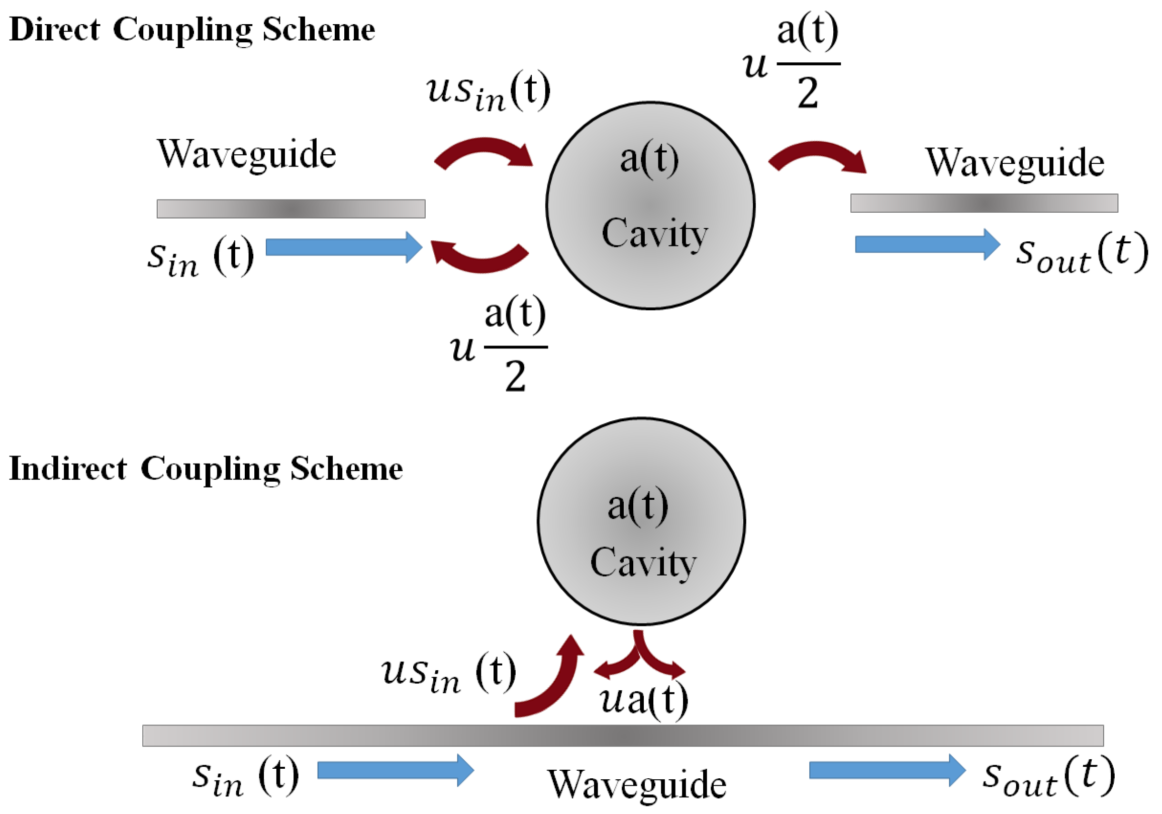
The standard modulation process of LiNbO3 modulator is fundamentally very different to the process undergone in photonic crystal cavity modulators. Here, a mismatch between the cavity resonance and the propagating wave will either cause transmission or reflection, depending on the implemented scheme. In this paper, two intensity modulation schemes are analyzed; direct and side coupling, as shown in Figure 1. In the direct coupling scheme, the transmitted power is proportional to the energy inside the cavity, this will decrease the achievable contrast ratio. This scheme will also lead to the transmitted power having a similar pulse shape to the control light. However, in the side coupled scheme, interference between the decaying wave from the cavity and the propagating wave in the waveguide mean a higher contrast ratio and variable pulse shape. In both schemes, an increase in the optical excitation power leads to a larger cavity resonance shift, this has a large effect on the pulse shape of the carrier wave and the sidebands produced from the modulation process. By arranging two or more PhC IMs in either a series or parallel formation, it is possible to increase the number of generated sidebands and hence observe an OFC. In this paper, detailed analysis of the different modulation schemes will be undertaken. This analysis will confirm that an OFC can be produced from a PhC device, thus broadening the application of PhC devices into the mature and prosperous research field of OFC generation.
2. Materials and Methods
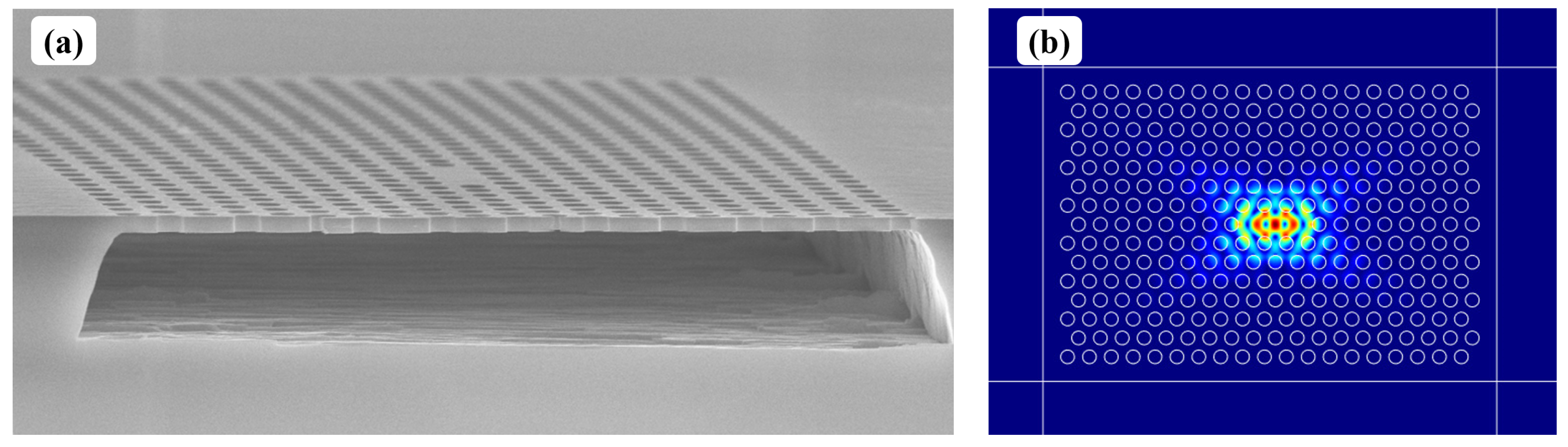
The scheme proposed here is based on photonic crystal waveguides and cavities to construct all-optical intensity modulators, as shown in Figure 1. This method of all-optical modulation has been studied in great detail by different research groups [12,13,14,15], which has led to a rich and common understanding of the fundamental principles behind PhC switches. PhC cavities have a very high quality factor (Q) while maintaining a low mode volume (V). This means that nonlinearity within the cavity can be greatly enhanced, given that the field intensity scales with Q/V. A shift in the cavity resonant wavelength, due to a refractive index change, is therefore possible with a relatively low-power pump light. Intensity modulation of a carrier light is therefore possible when a pump light is used to change the transmission wavelength. The device itself is made up of holes in triangular lattice formation fabricated in an InP membrane with embedded InAs quantum dots (QDs), with broad band emission around 1550 nm. The waveguides are made up of a line of missing holes and the cavity consists of a three hole defect, known as an L3 cavity, as shown in Figure 2. To ensure the cavity has a resonant frequency around 1550 nm the filling factor and lattice constant have been carefully calculated. The lattice constant is calculated to be 480 nm and the filling factor at 0.29. The thickness of the membrane will be 220 nm. The parameters given were calculated in COMSOL by finding the eigenfrequency via the finite element method (FEM). A scanning electron microscope (SEM) image of an L3 cavity along with the FEM simulation results for an L3 cavity with a fundamental mode at 1550 nm is shown in Figure 2.
Coupled mode theory (CMT), a standard PhC analysis tool, is used in this paper to simulate the device described above. The equations employed in this paper are based on an extension of CMT models that have been presented previously [13,16,17]. In the simulated device, it is assumed that an active region is present in the form of InAs QDs. This will lead to a dominating third order nonlinearity process based on the saturable absorption (SA) of QDs. Therefore, the refractive index change will be dominated by the Kramers–Kronig relation to the absorption coefficient. This has a direct relation to the field amplitude within the photonic crystal cavity and hence will be the main dynamic variable used throughout. A pump and carrier light are injected into the input waveguide, denoted by in Figure 1. The dynamical equations for the cavity modes is written as:
Here, ap,c is the amplitude of the cavity mode which is excited by the pump and carrier light, respectively and the energy inside the cavity is represented by |ap,c(t)|2. The field of the cavity is represented by
and the input light through the waveguide is given by
, the power of the light is represented by
. It is assumed that ap is far higher than ac, such that only ap will have an effect on the cavity resonance shift. ωp,c is the angular frequency of the input pulses, for either the pump or carrier light. In order for the cavity resonance to change, the amplitude of the pump light must increase. The change is then dependent on the energy in the cavity due to the pump light and a third order non-linearity, denoted as the Kerr constant. This is given below:
n2 is the enhanced Kerr coefficient, due to the SA of QDs in the membrane structure and the average rate of SA within the cavity is calculated and given by Vkerr. These values are greatly enhanced by the PhC cavity due to the small mode volume and high Q attainable in PhC structures. neff is the effective refractive index, this due to the membrane thickness, material properties and resonant wavelength of the cavity. The total loss rate in the cavity is split into two parts; the intrinsic loss, γint, and the coupling loss, γc. The intrinsic loss due to coupling into non-relevant modes, predominantly by vertical emission, is dependent on the Q factor of the cavity, such that γint = ω0/2Q. The coupling loss is due to the coupling coefficient between the cavity and the waveguide. The light in the L3 cavity will reflect off each side of the cavity in the longitudinal direction which leads to light coupling to the waveguide at each end, hence 2γc.
In order to induce a change in the transmission through the device, a change in the refractive index is needed. The amount that the refractive index must shift by is dependent on the linewidth of the cavity mode. In the device simulated here, a resonance shift of 1 nm will cause the carrier light to either reflect or transmit through the device. To obtain a shift of 1 nm, it is calculated that a refractive index shift of 0.005 is needed. The relationship between refractive index change and cavity resonance change is defined as = . Therefore, the profile of the refractive index change is in relation to the profile of the pump light, as given in Equation (1) and shown by the dashed line in Figure 3. Achieving a refractive index change of 0.005 using QD saturable absorption as the refractive index non-linearity is common among nanophotonics research community [18,19].
3. Results and Discussion
As discussed earlier, two common cavity-waveguide all-optical modulator configurations have been considered in this paper: side and direct cavity coupling; these are schematically represented in Figure 1. Given that the waveguide is unbroken in the side coupling scheme, the output will be dependent on both the cavity energy and the energy in the waveguide, giving rise to Equation (4) and the green line in Figure 3.
The coupling factor, u, is defined as u = [21]. In the direct coupling scheme the output will only rely on the energy in the cavity due to the carrier pump, such that:
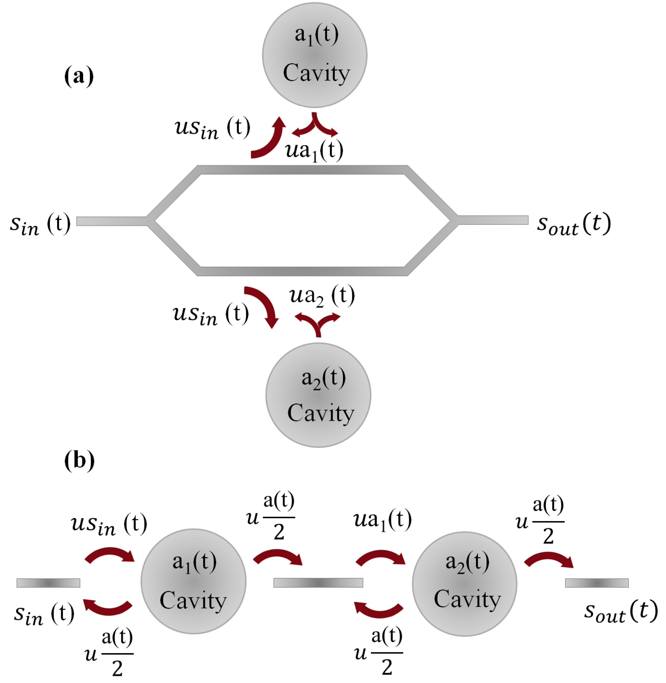
The output of this is shown by the solid purple line in Figure 3. The control light has a sinusoidal wave form with a repetition frequency in the GHz range, as shown in Figure 3. This leads to different output dynamics for the carrier light, depending on which scheme is used. In this paper, the PhC-based IMs are cascaded in both series and parallel in order to generate an OFC, as shown in Figure 4. When two IMs are in parallel with each other, it is assumed that the carrier light is split evenly into each arm. Each arm is then coupled to a cavity via the side coupling scheme, as shown in Figure 4 and when they recombine, the output is given by:
where represents the input to the bottom or top cavity and represents the amplitude of the carrier signal in the bottom or top cavity. When two IMs are put in parallel with each other, as shown in Figure 4a, and the phase of the modulating wave in each arm can be controlled, it displays properties similar to that of a conventional IM. The PhC design, outlined in Figure 4a, consists of a waveguide leading into a Y junction symmetric splitter [22,23], where the pump and carrier light split evenly into each arm. An L3 cavity is coupled to each arm of the device to induce intensity modulation of the split carrier light. The two intensity modulated carrier lights then recombine via a Y junction to produce a dual modulated carrier signal. This technique of waveguide splitting and recombining in PhC waveguides is common when implementing PhC-based Mach–Zehnder interferometers [24,25]. Using this process, the shape of the carrier light will be determined by a number of parameters unique to this type of modulation, these include the phase shift of the pump light in each arm, the coupling efficiency of the light into the cavity and the Q factor of the cavity.
This method of modulation can generate 3 comb lines with a maximum intensity difference of 1 dB on each side of the central carrier frequency, hence 7 comb lines all together as shown in Figure 5b. Additional comb lines exist at much weaker intensities further away from the initial carrier frequency. The number of generated intensity spikes in the frequency domain is limited by the attainable modulation profile of the carrier light in the time domain. As can be seen, the carrier wavelength has a much stronger intensity than the sidebands produced. Nevertheless, the homogeneity in intensity between the sidebands remains very uniform. The homogeneity of these sidebands is dependent on the parameters stated above and can therefore be optimized to generate a comb, as shown in Figure 5b. During experimental implementation of the proposed scheme, there will be disparity between the optimised parameters given here and the fabricated device. Although this will have an effect on the OFC quality, it is expected that a 7 line OFC can be observed for a broad range of parameter values. Figure 5a shows that for Q factors between 10,000 and 25,000 the side band intensity fluctuates to a maximum of 1.5 dB. This shows that a wide range of Q factor values will still achieve a 7 line OFC. The extinction ratio of the carrier signal is dominated by the coupling factor between the cavity and the waveguide. This will have an effect on the intensity of the generated comb lines relative to the intensity of the central carrier frequency. However, 3 sidebands on either side of the initial carrier frequency can still be generated for a broad range of coupling factors.
Figure 5a shows the effect the Q factor has on the uniformity with an optimum Q factor of 13,000. This is due to the shape of the carrier light through each arm when it recombines to generate the intensity modulated signal. Cavity Q factors in PhC L3 cavities can be greatly enhanced by altering the position of the holes surrounding the L3 cavity [26]. It is therefore possible to design the L3 cavity with the desired Q factor via fine tuning of the hole positions. The 7 comb lines observed have with a maximum fluctuation in intensity of less than 1 dB if the carrier frequency is not taken into consideration. In previous work, the intensity of the initial carrier frequency has also posed a problem in modulation-based combs [27] and micro-cavity-based combs, due to the high energy needed to induce nonlinearity within the micro-cavity [28]. A method to overcome this is to include a cavity-based notch filter. To obtain the required suppression of the carrier signal the coupling coefficient, size and loss coefficient of the cavity can be determined via calculation. The filter will induce an overall loss to the carrier wave signal of around 5 dB, but the flatness of the 7-line OFC will be greatly enhanced.
When two IMs are in series with each other, as shown in Figure 4b, the output from the first IM will be the input for the second. The equation for the energy inside the second cavity is given by:
The output of the second cavity is equivalent to the output of the single cavity device, as given in Equation (5). In the parallel scheme outlined above, side coupled cavities were used to generate an OFC because a broad pulse was able to be produced from a sinusoidal control light. The high extinction ratio and pulse shape gained from this scheme meant a short, high intensity pulse could be produced and generate an OFC. However, in order to produce an OFC from two IMs in parallel, the sinusoidal pulse shape at the output of the IM is more desirable. Sidebands are produced in the frequency domain from the initial carrier light by a single IM with a sinusoidal pump light profile [29]. This is shown in Figure 6a where a sideband either side of the initial carrier frequency has been generated. The sideband intensity is within 5 dB of the carrier intensity and their FSR is in direct relation to the modulation frequency. The sidebands produced from the first IM then act as carrier waves leading into the second IM. The second IM has a modulation frequency one third that of the first, meaning that the generated sidebands will have an FSR one third that of the original FSR. Two extra comb lines are generated on each side of the carrier frequency; they are the sum of the generated sidebands from both the initial carrier frequency and the initial sidebands generated from a single IM.
This scheme then generates multiple sidebands that are of equal distance from each other in the frequency domain and of similar intensity. In this scheme, 7 comb lines have been generated, Figure 6b shows the generated OFC, while Figure 6a shows sideband generation from a single IM, in which the FSR is directly related to the repetition rate of the modulating signal. In this case, this is within the microwave range, at around 10 GHz. A microwave signal is then generated from the beat note between the carrier and the sideband, this is a common tool in microwave photonics [30].
4. Conclusions
To conclude, a new and novel approach to OFC generation using PhC structures is proposed. By integrating multiple PhC cavities, it is possible to observe OFC generation on the nanoscale. A model based on CMT is built upon to simulate the modulation of a carrier light through a PhC modulator using a pump light with a repetition rate in the RF range. By cascading multiple cavities in either series or parallel, sidebands in the frequency response of the carrier wave can be observed. By careful manipulation of the device parameters, these sidebands can be optimised to give a flat spectrum across 7 comb lines. Using the parallel-based scheme, the Q factor of both cavities can be specified to give a flat comb over the generated sidebands. However, the initial carried frequency will have a far greater intensity, which could limit the OFC operation. To overcome this, it is possible to use a specifically designed notch filter. Using a scheme with two cavities in series, it is possible to generate a flatter comb across all lines without the need for a notch filter. In this scheme, two separate RF lines are needed to drive each cavity separately, which will cause complexity within the system.
PhC devices are a mature enough research field that fabrication techniques are commonplace to many institutes; therefore, implementation of this technique experimentally is very promising. PhC devices based on cavities and waveguides are a well-established and rich research field which have the potential to enable on chip photonic networks. To this end, the device proposed here will contribute towards both the field of PhCs as well as expanding OFC generation techniques into a new domain.
Author Contributions
Conceptualization, H.F. and C.J.; methodology, K.C. and S.C.; software, H.F., K.C. and S.C.; validation, C.J., M.H. and K.C.; investigation, H.F.; resources, C.J.; writing–original draft preparation, H.F.; writing–review and editing, C.J. and M.H.; visualization, H.F and C.J.; supervision, C.J. and M.H.
Funding
This research was funded by EPSRC First Grant, the Royal Society Research Grant (UK) and NSFC Grant No. 61574138 and No. 61974131 (China).
Conflicts of Interest
The authors declare no conflict of interest.
Abbreviations
The following abbreviations are used in this manuscript:
| PhC | Photonic Crystal |
| OFC | Optical Frequency Comb |
| FEM | Finite Element Method |
| SEM | Scanning Electron Microscope |
| FSR | Free Spectral Range |
| CMT | Coupled Mode Theory |
| QD | Quantum Dot |
References
- Gaeta, A.L.; Lipson, M.; Kippenberg, T.J. Photonic-chip-based frequency combs. Nat. Photonics 2019, 13. [Google Scholar] [CrossRef]
- Pasquazi, A.; Peccianti, M.; Razzari, L.; Moss, D.J.; Coen, S.; Erkintalo, M.; Chembo, Y.K.; Hansson, T.; Wabnitz, S.; Del’Haye, P.; et al. Micro-combs: A novel generation of optical sources. Phys. Rep. 2017, 729, 1–81. [Google Scholar] [CrossRef]
- Demirtzioglou, I.; Lacava, C.; Bottrill, K.R.H.; Thomson, D.J.; Reed, G.T.; Richardson, D.J.; Petropoulos, P. Frequency comb generation in a silicon ring resonator modulator. Opt. Express 2018, 26, 790. [Google Scholar] [CrossRef] [PubMed]
- Diddams, S.A. The evolving optical frequency comb. J. Opt. Soc. Am. 2010, 27, B51–B62. [Google Scholar] [CrossRef]
- Udem, T.; Holzwarth, R.; Hansch, T.W. Optical frequency metrology. Nature 2002, 416, 233–237. [Google Scholar] [CrossRef] [PubMed]
- Torres-Company, V.; Lancis, J.; Andres, P. Lossless equalization of frequency combs. Opt. Lett. 2008, 33, 1822–1824. [Google Scholar] [CrossRef] [PubMed]
- Spencer, D.T.; Drake, T.; Briles, T.C.; Stone, J.; Sinclair, L.C.; Fredrick, C.; Li, Q.; Westly, D.; Ilic, B.R.; Bluestone, A.; et al. An optical-frequency synthesizer using integrated photonics. Nature 2018, 557, 81–85. [Google Scholar] [CrossRef] [PubMed]
- Chembo, Y.K. Kerr optical frequency combs: Theory, applications and perspectives. Nanophotonics 2016, 5, 214–230. [Google Scholar] [CrossRef]
- Razzari, L.; Duchesne, D.; Ferrera, M.; Morandotti, R.; Chu, S.; Little, B.E.; Moss, D.J. CMOS-compatible integrated optical hyper-parametric oscillator. Nat. Photonics 2010, 4, 41–45. [Google Scholar] [CrossRef]
- Shang, L.; Wen, A.; Lin, G.; Gao, Y. A fl at and broadband optical frequency comb with tunable bandwidth and frequency spacing. Opt. Commun. 2014, 331, 262–266. [Google Scholar] [CrossRef]
- Healy, T.; Gunning, F.C.G.; Ellis, A.D.; Bull, J.D. Multi-wavelength source using low drive-voltage amplitude modulators for optical communications. Opt. Express 2007, 15, 2981–2986. [Google Scholar] [PubMed]
- Nozaki, K.; Tanabe, T.; Shinya, A.; Matsuo, S.; Sato, T.; Taniyama, H.; Notomi, M. Sub-femtojoule all-optical switching using a photonic-crystal nanocavity. Nat. Photonics 2010, 4, 477–483. [Google Scholar] [CrossRef]
- Yu, Y.; Palushani, E.; Heuck, M.; Kuznetsova, N.; Kristensen, P.T.; Ek, S.; Vukovic, D.; Peucheret, C.; Oxenløwe, L.K.; Combrié, S.; et al. Switching characteristics of an InP photonic crystal nanocavity: Experiment and theory. Opt. Express 2013, 21, 31047. [Google Scholar] [CrossRef] [PubMed]
- Notomi, M.; Shinya, A.; Mitsugi, S.; Kira, G.; Kuramochi, E.; Tanabe, T. Optical bistable switching action of Si high-Q photonic-crystal nanocavities. Opt. Express 2005, 13, 2678. [Google Scholar] [CrossRef] [PubMed]
- Jin, C.Y.; Johne, R.; Swinkels, M.Y.; Hoang, T.B.; Midolo, L.; Van Veldhoven, P.J.; Fiore, A. Ultrafast non-local control of spontaneous emission. Nat. Nanotechnol. 2014, 9, 886–890. [Google Scholar] [CrossRef] [PubMed] [Green Version]
- Uesugi, T.; Song, B.S.; Asano, T.; Noda, S. Investigation of optical nonlinearities in an ultra-high-Q Si nanocavity in a two-dimensional photonic crystal slab. Opt. Express 2006, 14, 377–386. [Google Scholar] [CrossRef]
- De Rossi, A.; Lauritano, M.; Combrié, S.; Tran, Q.V.; Husko, C. Interplay of plasma-induced and fast thermal nonlinearities in a GaAs-based photonic crystal nanocavity. Phys. Rev. At. Mol. Opt. Phys. 2009, 79, 1–9. [Google Scholar] [CrossRef]
- Jin, C.Y.; Wada, O. Photonic switching devices based on semiconductor nano-structures. J. Phys. Appl. Phys. 2014, 47. [Google Scholar] [CrossRef]
- Prasanth, R.; Haverkort, J.E.; Deepthy, A.; Bogaart, E.W.; Van Der Tol, J.J.; Patent, E.A.; Zhao, G.; Gong, Q.; Van Veldhoven, P.J.; Nötzel, R.; et al. All-optical switching due to state filling in quantum dots. Appl. Phys. Lett. 2004, 84, 4059–4061. [Google Scholar] [CrossRef] [Green Version]
- Sauvage, S.; Boucaud, P.; Glotin, F.; Prazeres, R.; Ortega, J.M.; Lemaître, A.; Gérard, J.M.; Thierry-Mieg, V. Third-harmonic generation in InAs/GaAs self-assembled quantum dots. Phys. Rev. Condens. Matter Mater. Phys. 1999, 59, 9830–9833. [Google Scholar]
- Joannopoulos, J.; Johnson, S.; Winn, J.; Meade, R. Photonic Crystals: Molding the Flow of Light, 2nd ed.; Princeton University Press: Princeton, NJ, USA, 2008. [Google Scholar]
- Boscolo, S.; Midrio, M. Y junctions in photonic crystal channel waveguides: High transmission and impedance matching. Opt. Lett. 2002, 27, 1001–1003. [Google Scholar] [PubMed]
- Turner, J.S.; Lourtioz, J.M.; Berger, V.; Gérard, J.M.; Tchelnokov, A. Photonic Crystals, 2nd ed.; Springer: Berlin/Heidelberg, Germany, 2008. [Google Scholar]
- Martinez, A.; Sanchis, P.; Marti, J. Mach – Zehnder interferometers in photonic crystals. Opt. Quantum Electron. 2005, 37, 77–93. [Google Scholar] [CrossRef]
- Nakamura, H.; Sugimoto, Y.; Kanamoto, K.; Ikeda, N.; Tanaka, Y.; Nakamura, Y.; Ohkouchi, S.; Watanabe, Y.; Inoue, K.; Ishikawa, H.; et al. Ultra-fast photonic crystal/quantum dot all- optical switch for future photonic networks. Opt. Express 2004, 12, 6606–6614. [Google Scholar]
- Chalcraft, A.R.; Lam, S.; O’Brien, D.; Krauss, T.F.; Sahin, M.; Szymanski, D.; Sanvitto, D.; Oulton, R.; Skolnick, M.S.; Fox, A.M.; et al. Mode structure of the L3 photonic crystal cavity. Appl. Phys. Lett. 2007, 90, 1–4. [Google Scholar] [CrossRef]
- Nagarjun, K.P.; Vadivukarassi, J.; Kumar, S.; Supradeepa, S. Generation of tunable, high repetition rate frequency combs with equalized spectra using carrier injection-based silicon modulators. Opt. Express 2018, 26, 975218. [Google Scholar] [CrossRef]
- Kippenberg, T.J.; Holzwarth, R.; Diddams, S.A. Microresonator-Based Optical Frequency Combs. Science 2011, 332, 555–560. [Google Scholar] [CrossRef] [PubMed]
- Francis, H.; Chen, S.; Ho, C.H.; Che, K.J.; Wang, Y.R.; Hopkinson, M.; Jin, C.Y. Generation of optical frequency combs using a photonic crystal cavity. IET Optoelectron. 2018, 13, 23–26. [Google Scholar] [CrossRef]
- Yao, J. Microwave Photonics. J. Light. Technol. 2014, 27, 314–335. [Google Scholar] [CrossRef]
Figure 1.
The two all-optical intensity modulator schemes studied in this paper. a(t) is the cavity field amplitude, u is the coupling factor, and sin (t) and sout (t) represent the amplitude of the propagating wave in the input and output waveguide, respectively.
Figure 1.
The two all-optical intensity modulator schemes studied in this paper. a(t) is the cavity field amplitude, u is the coupling factor, and sin (t) and sout (t) represent the amplitude of the propagating wave in the input and output waveguide, respectively.

Figure 2.
(a) An scanning electron microscope (SEM) image of a photonic crystal membrane with an L3 cavity in the center. (b) Finite element method (FEM) calculation of the fundamental mode at 1550 nm.
Figure 2.
(a) An scanning electron microscope (SEM) image of a photonic crystal membrane with an L3 cavity in the center. (b) Finite element method (FEM) calculation of the fundamental mode at 1550 nm.

Figure 3.
The power of the carrier wave at the output of the device is given by the solid lines. The refractive index change inside the cavity is given by the dotted line.
Figure 3.
The power of the carrier wave at the output of the device is given by the solid lines. The refractive index change inside the cavity is given by the dotted line.

Figure 4.
Schematics for the proposed photonic crystal (PhC) all-optical optical frequency combs (OFC) generators. (a) Two side coupled cavity modulators in parallel. (b) Two direct coupled cavity modulators in series.
Figure 4.
Schematics for the proposed photonic crystal (PhC) all-optical optical frequency combs (OFC) generators. (a) Two side coupled cavity modulators in parallel. (b) Two direct coupled cavity modulators in series.

Figure 5.
(a) Homogeneity between the sidebands against the cavity Q factor. (b) The generated OFC.

Figure 6.
(a) The frequency response of the carrier wave after a single direct coupled intensity modulators (IM). (b) The generated OFC from two all-optical PhC direct coupled modulators in series.
Figure 6.
(a) The frequency response of the carrier wave after a single direct coupled intensity modulators (IM). (b) The generated OFC from two all-optical PhC direct coupled modulators in series.


Table 1.
Physical parameters used in coupled mode theory (CMT) calculations.
| Parameter | Symbol | Value | Source |
|---|---|---|---|
| Coupling loss | γc | 1 × 10¹¹ | Estimated |
| Cavity quality factor | Q | 10,000 | FEM calculation |
| Effective refractive index | neff | 3.1 | [13] |
| Intrinsic loss | γint | 1.1 × 10¹¹ | Calculated |
| Kerr coefficient | n2 | 1.5 × 10⁻¹⁴ m2/W | [20] |
| Kerr mode volume | VKerr | 0.21 m3 | Calculated [16] |
| Resonant wavelength | ω0 | 1.550 m | Calculated |
© 2019 by the authors. Licensee MDPI, Basel, Switzerland. This article is an open access article distributed under the terms and conditions of the Creative Commons Attribution (CC BY) license (http://creativecommons.org/licenses/by/4.0/).
Share and Cite
MDPI and ACS Style
Francis, H.; Chen, S.; Che, K.-J.; Hopkinson, M.; Jin, C. Photonic Crystal Cavity-Based Intensity Modulation for Integrated Optical Frequency Comb Generation. Crystals 2019, 9, 493. https://0-doi-org.brum.beds.ac.uk/10.3390/cryst9100493
AMA Style
Francis H, Chen S, Che K-J, Hopkinson M, Jin C. Photonic Crystal Cavity-Based Intensity Modulation for Integrated Optical Frequency Comb Generation. Crystals. 2019; 9(10):493. https://0-doi-org.brum.beds.ac.uk/10.3390/cryst9100493
Chicago/Turabian StyleFrancis, Henry, Si Chen, Kai-Jun Che, Mark Hopkinson, and Chaoyuan Jin. 2019. "Photonic Crystal Cavity-Based Intensity Modulation for Integrated Optical Frequency Comb Generation" Crystals 9, no. 10: 493. https://0-doi-org.brum.beds.ac.uk/10.3390/cryst9100493
Note that from the first issue of 2016, this journal uses article numbers instead of page numbers. See further details here.