Ultra-High Light Extraction Efficiency and Ultra-Thin Mini-LED Solution by Freeform Surface Chip Scale Package Array

 , ,
, , 
Abstract
:1. Introduction
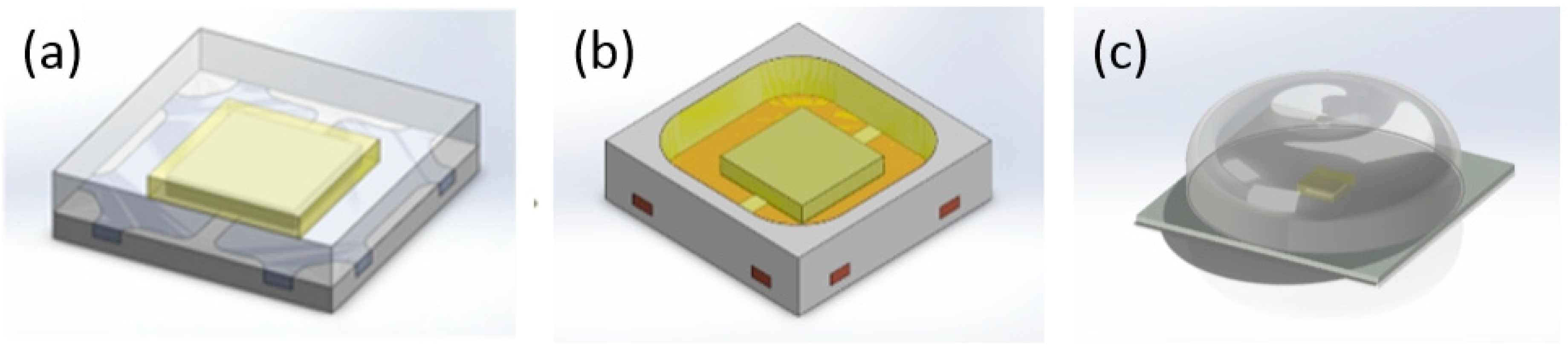
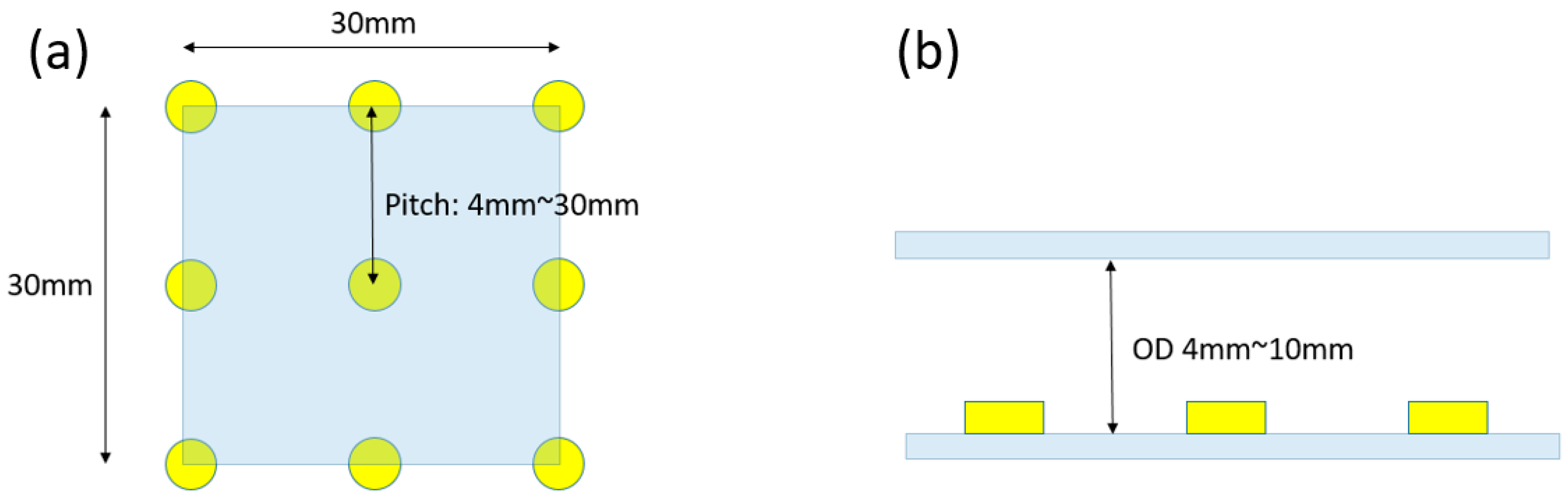
2. Experiment
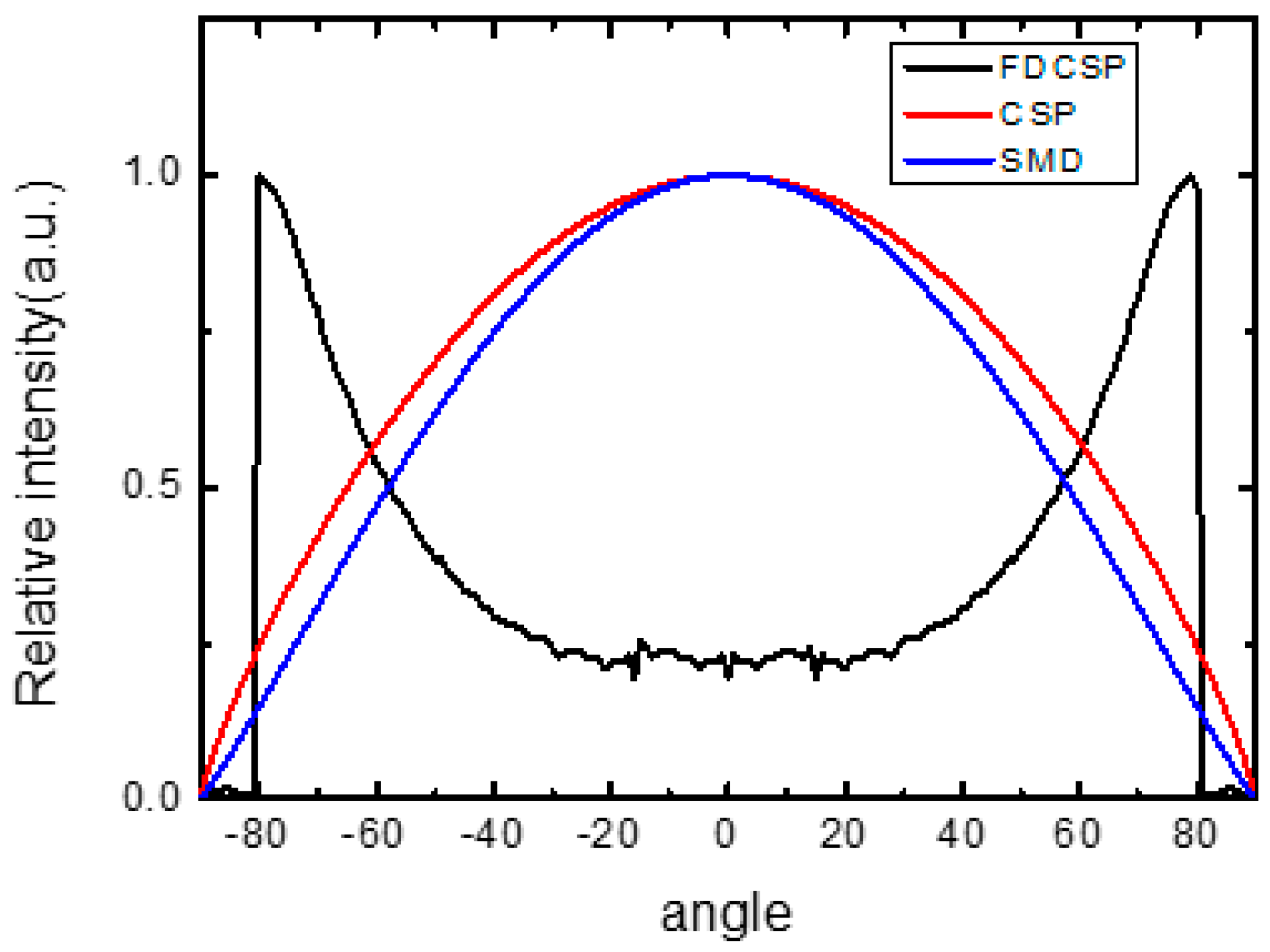
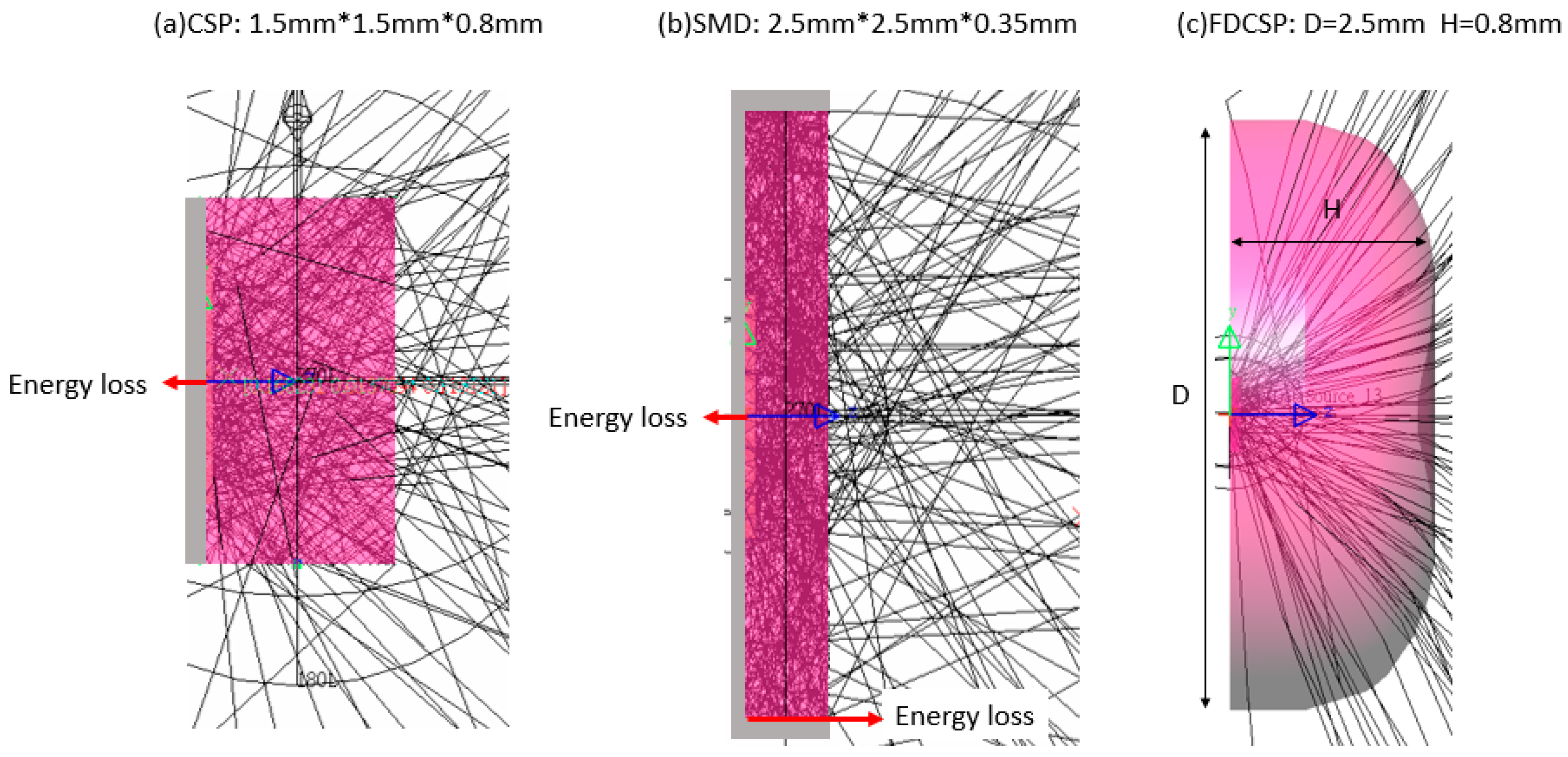
3. Result and Discussion
4. Conclusions
Author Contributions
Funding
Conflicts of Interest
References
- Francois, E.; Fogg, C.; He, Y.W.; Li, X.; Luthra, A.; Segall, A. High dynamic range and wide color gamut video coding in hevc: Status and potential future enhancements. IEEE Trans. Circuits Syst. Video Technol. 2016, 26, 63–75. [Google Scholar] [CrossRef]
- Chen, H.W.; Zhu, R.D.; Li, M.C.; Lee, S.L.; Wu, S.T. Pixel-by-pixel local dimming for high-dynamic-range liquid crystal displays. Opt. Express 2017, 25, 1973–1984. [Google Scholar] [CrossRef]
- Chen, H.F.; Ha, T.H.; Sung, J.H.; Kim, H.R.; Han, B.H. Evaluation of LCD local-dimming-backlight system. J. Soc. Inf. Disp. 2010, 18, 57–65. [Google Scholar] [CrossRef]
- Krause, M.; Riplinger, M.; Louis, A.K.; Xu, C.H. A new class of very efficient algorithms for local dimming. Optim. Eng. 2018, 19, 1–17. [Google Scholar] [CrossRef]
- Raypah, M.E.; Sodipo, B.K.; Devarajan, M.; Sulaiman, F. Estimation of optical power and heat-dissipation factor of low-power SMD LED as a function of injection current and ambient temperature. IEEE Trans. Electron Devices 2016, 63, 408–413. [Google Scholar] [CrossRef]
- Huang, C.H.; Chen, K.J.; Tsai, M.T.; Shih, M.H.; Sun, C.W.; Lee, W.I.; Lin, C.C.; Kuo, H.C. High-efficiency and low assembly-dependent chip-scale package for white light-emitting diodes. J. Photonics Energy 2015, 5, 057606. [Google Scholar] [CrossRef]
- Lee, K.H.; Kim, S.H.; Lim, W.S.; Song, J.O.; Ryou, J.H. Visible light-emitting diodes with thin-film-flip-chip-based wafer-level chip-scale package technology using anisotropic conductive film bonding. IEEE Electron Device Lett. 2015, 36, 702–704. [Google Scholar] [CrossRef]
- Lee, K.H.; Asadirad, M.; Shervin, S.; Oh, S.K.; Oh, J.T.; Song, J.O.; Moon, Y.T.; Ryou, J.H. Thin-film-flip-chip LEDs grown on Si substrate using wafer-level chip-scale package. IEEE Photonics Technol. Lett. 2016, 28, 1956–1959. [Google Scholar] [CrossRef]
- Lin, C.H.; Pai, Y.M.; Kang, C.Y.; Lin, H.Y.; Lee, C.F.; Chen, X.Y.; Tu, H.H.; Yang, J.J.; Chen, C.H.; Lin, C.C.; et al. Square column structure of high efficiency, reliable, uniformly flexible LED devices. Crystals 2018, 8, 472. [Google Scholar] [CrossRef]
- Gou, F.W.; Hsiang, E.L.; Tan, G.J.; Lan, Y.F.; Tsai, C.Y.; Wu, S.T. Tripling the optical efficiency of color-converted micro-LED displays with funnel-tube array. Crystals 2019, 9, 39. [Google Scholar] [CrossRef]
- Jiang, H.X.; Lin, J.Y. Nitride micro-LEDs and beyond—A decade progress review. Opt. Express 2013, 21, A475–A484. [Google Scholar] [CrossRef] [PubMed]
- Liu, Z.J.; Chong, W.C.; Wong, K.M.; Lau, K.M. Gan-based LED micro-displays for wearable applications. Microelectron. Eng. 2015, 148, 98–103. [Google Scholar] [CrossRef]
- Zheng, L.L.; Guo, Z.Q.; Yan, W.; Lin, Y.; Lu, Y.J.; Kuo, H.C.; Chen, Z.; Zhu, L.H.; Wu, T.Z.; Gao, Y.L. Research on a camera-based microscopic imaging system to inspect the surface luminance of the micro-LED array. IEEE Access 2018, 6, 51329–51336. [Google Scholar] [CrossRef]
- Huang Chen, S.-W.; Shen, C.-C.; Wu, T.; Liao, Z.-Y.; Chen, L.-F.; Zhou, J.-R.; Lee, C.-F.; Lin, C.-H.; Lin, C.-C.; Sher, C.-W.; et al. Full-color monolithic hybrid quantum dot nanoring micro light-emitting diodes with improved efficiency using atomic layer deposition and nonradiative resonant energy transfer. Photonics Res. 2019, 7, 416–422. [Google Scholar] [CrossRef]
- Corbett, B.; Loi, R.; Zhou, W.; Liu, D.; Ma, Z. Transfer print techniques for heterogeneous integration of photonic components. Prog. Quant. Electron. 2017, 52, 1–17. [Google Scholar] [CrossRef]
- Wu, T.Z.; Sher, C.W.; Lin, Y.; Lee, C.F.; Liang, S.J.; Lu, Y.J.; Chen, S.W.H.; Guo, W.J.; Kuo, H.C.; Chen, Z. Mini-LED and micro-LED: Promising candidates for the next generation display technology. Appl. Sci. 2018, 8, 1557. [Google Scholar] [CrossRef]
- Tan, G.J.; Huang, Y.G.; Li, M.C.; Lee, S.L.; Wu, S.T. High dynamic range liquid crystal displays with a mini-LED backlight. Opt. Express 2018, 26, 16572–16584. [Google Scholar] [CrossRef]
- Huang, W.T.; Cheng, C.L.; Bao, Z.; Yang, C.W.; Lu, K.M.; Kang, C.Y.; Lin, C.M.; Liu, R.S. Broadband Cr3+, Sn4+-doped oxide nanophosphors for infrared mini light-emitting diodes. Angew. Chem. Int. Ed. 2019, 58, 2069–2072. [Google Scholar] [CrossRef]
- Kim, B.; Kim, J.; Ohm, W.S.; Kang, S. Eliminating hotspots in a multi-chip LED array direct backlight system with optimal patterned reflectors for uniform illuminance and minimal system thickness. Opt. Express 2010, 18, 8595–8604. [Google Scholar] [CrossRef]
- Rao, R.; Mos, B.; Overes, T.; Langendijk, E.H.A. Masking LED hot spots in a thin direct lit backlight unit using semitransparent and perforated masks. Opt. Commun. 2014, 315, 258–264. [Google Scholar] [CrossRef]
- Sekiguchi, Y.; Konno, A.; Tsumura, M. Design method for a thin uniform direct backlight using a diffuser plate with a pattern on the surface and optical films. Appl. Opt. 2015, 54, 482–491. [Google Scholar] [CrossRef]


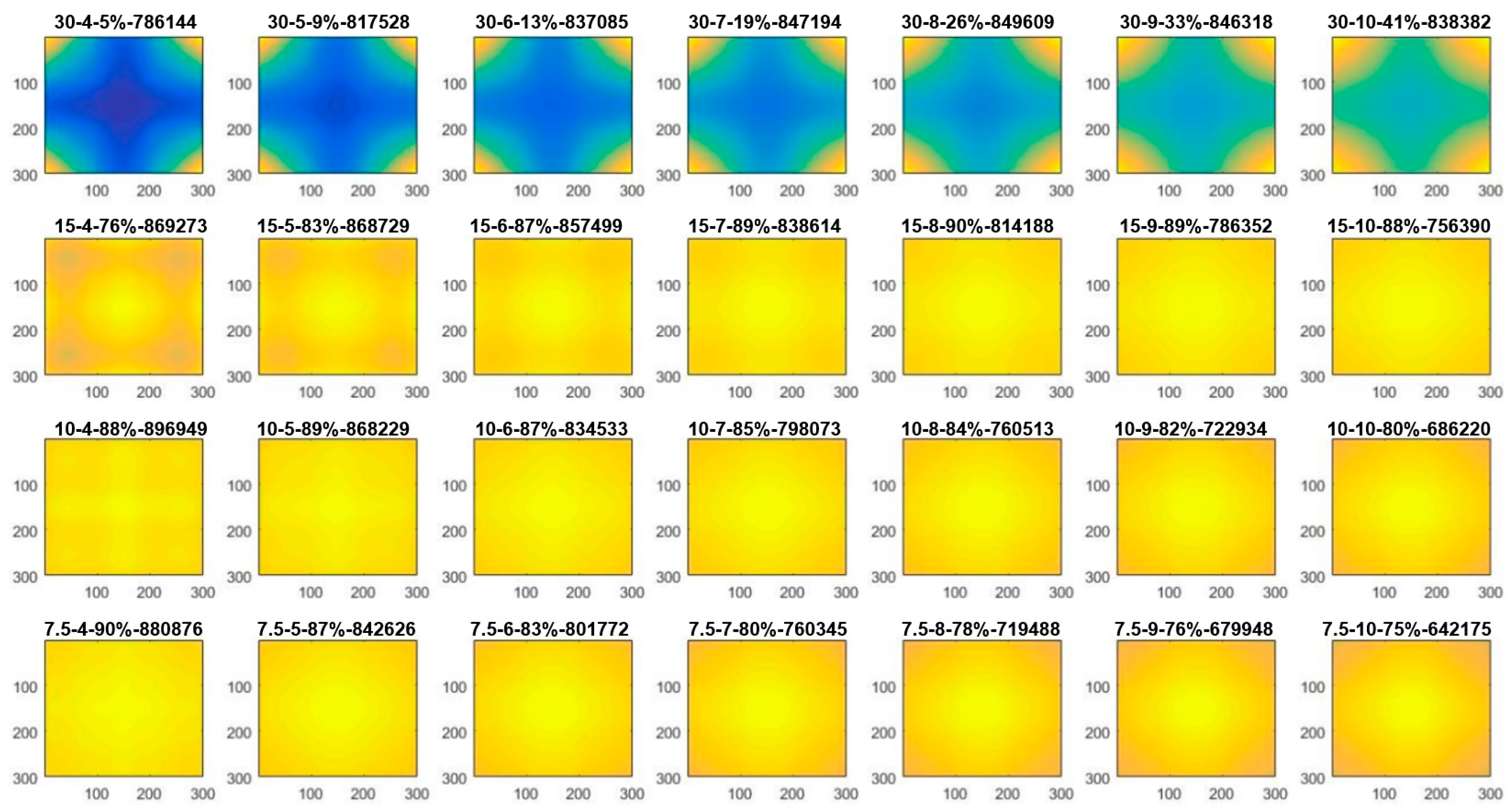
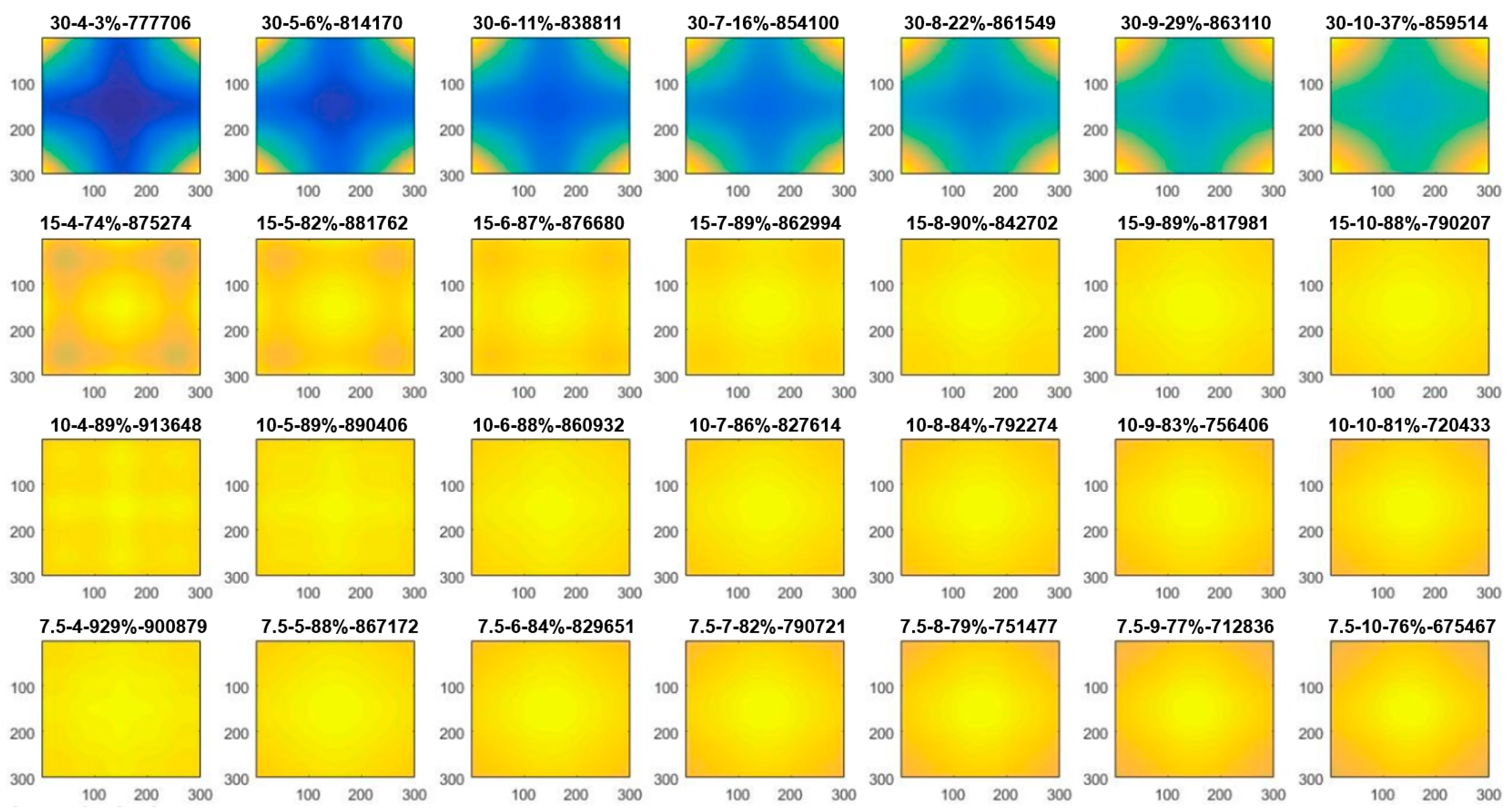
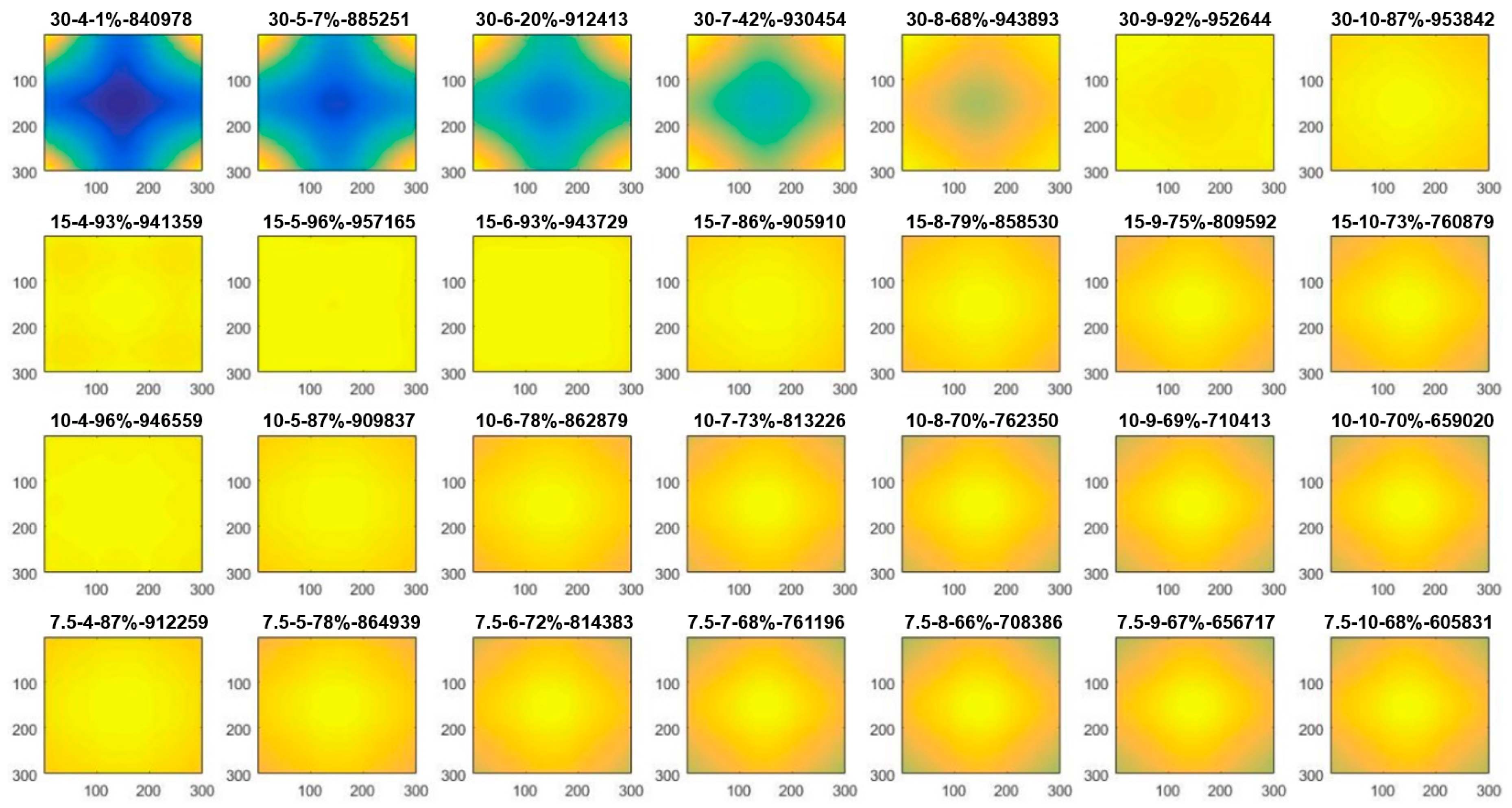
| Pitch (mm) | OD (mm) | Uniformity-CSP (%) | Uniformity-SMD (%) | Uniformity-FDCSP (%) | Intensity-CSP (a.u.) | Intensity-SMD (a.u.) | Intensity-FDCSP (a.u.) |
|---|---|---|---|---|---|---|---|
| 30 | 4 | 5 | 3 | 1 | 100% | 67% | 117% |
| 30 | 5 | 9 | 6 | 7 | 104% | 71% | 123% |
| 30 | 6 | 13 | 11 | 20 | 106% | 73% | 127% |
| 30 | 7 | 19 | 16 | 42 | 108% | 74% | 129% |
| 30 | 8 | 26 | 22 | 68 | 108% | 75% | 131% |
| 30 | 9 | 33 | 29 | 92 | 108% | 75% | 132% |
| 30 | 10 | 41 | 37 | 87 | 107% | 75% | 132% |
| 15 | 4 | 76 | 74 | 93 | 111% | 76% | 131% |
| 15 | 5 | 83 | 82 | 96 | 111% | 76% | 133% |
| 15 | 6 | 87 | 87 | 93 | 109% | 76% | 131% |
| 15 | 7 | 89 | 89 | 86 | 107% | 75% | 126% |
| 15 | 8 | 90 | 90 | 79 | 104% | 73% | 119% |
| 15 | 9 | 89 | 89 | 75 | 100% | 71% | 112% |
| 15 | 10 | 88 | 88 | 73 | 96% | 69% | 106% |
| 10 | 4 | 88 | 89 | 96 | 114% | 79% | 131% |
| 10 | 5 | 89 | 89 | 87 | 110% | 77% | 126% |
| 10 | 6 | 87 | 88 | 78 | 106% | 75% | 120% |
| 10 | 7 | 85 | 86 | 73 | 102% | 72% | 113% |
| 10 | 8 | 84 | 84 | 70 | 97% | 69% | 106% |
| 10 | 9 | 82 | 83 | 69 | 92% | 66% | 99% |
| 10 | 10 | 80 | 81 | 70 | 87% | 62% | 91% |
| 7.5 | 4 | 90 | 92 | 87 | 112% | 78% | 127% |
| 7.5 | 5 | 87 | 88 | 78 | 107% | 75% | 120% |
| 7.5 | 6 | 83 | 84 | 72 | 102% | 72% | 113% |
| 7.5 | 7 | 80 | 82 | 68 | 97% | 69% | 106% |
| 7.5 | 8 | 78 | 79 | 66 | 92% | 65% | 98% |
| 7.5 | 9 | 76 | 77 | 67 | 86% | 62% | 91% |
| 7.5 | 10 | 75 | 76 | 68 | 82% | 59% | 84% |
| CSP | SMD | FDCSP | |
|---|---|---|---|
| PKG Efficiency | 88% | 60% | 96% |
| Angular | 130° Gaussian distribution | 120° Gaussian distribution | 160° Bat wing distribution |
| Array Efficiency @OD4 Pitch10mm | 111% | 76% | 131% |
| Solution Factor S S (85%, 60%) | 1.5 < S (85%, 60%) < 2.5 Max intensity: 112% Max OD = 10 | 1.4 < S (85%, 60%) < 2.5 Max intensity: 78% Max OD = 10 | 2.1 < S (85%, 60%) <3.75 Max intensity: 131% Max OD = 10 |
| Solution Factor S S (85%, 70%) | 1.5 < S (85%, 70%) < 2.5 Max intensity: 112% Max OD = 10 | 1.4 < S (85%, 70%) <2.5 Max intensity: 78% Max OD = 9 | 2.1 < S (85%, 70%) <3.75 Intensity: 131% Max OD = 10 |
| Solution Factor S S (85%, 100%) | 1.5 < S (85%, 100%) < 2.5 Max intensity: 112% Max OD = 9 | NA | 2.1 < S (85%, 100%) <3.75 Intensity: 131% Max OD = 10 |
| Solution Factor S S (85%, 110%) | 1.5 < S (85%, 110%) < 2.5 Max intensity: 112% Max OD = 5 | NA | 2.1 < S (85%, 110%) <3.75 Intensity: 131% Max OD = 10 |
© 2019 by the authors. Licensee MDPI, Basel, Switzerland. This article is an open access article distributed under the terms and conditions of the Creative Commons Attribution (CC BY) license (http://creativecommons.org/licenses/by/4.0/).
Share and Cite
Huang, C.-H.; Kang, C.-Y.; Chang, S.-H.; Lin, C.-H.; Lin, C.-Y.; Wu, T.; Sher, C.-W.; Lin, C.-C.; Lee, P.-T.; Kuo, H.-C. Ultra-High Light Extraction Efficiency and Ultra-Thin Mini-LED Solution by Freeform Surface Chip Scale Package Array. Crystals 2019, 9, 202. https://0-doi-org.brum.beds.ac.uk/10.3390/cryst9040202
Huang C-H, Kang C-Y, Chang S-H, Lin C-H, Lin C-Y, Wu T, Sher C-W, Lin C-C, Lee P-T, Kuo H-C. Ultra-High Light Extraction Efficiency and Ultra-Thin Mini-LED Solution by Freeform Surface Chip Scale Package Array. Crystals. 2019; 9(4):202. https://0-doi-org.brum.beds.ac.uk/10.3390/cryst9040202
Chicago/Turabian StyleHuang, Che-Hsuan, Chieh-Yu Kang, Shu-Hsiu Chang, Chih-Hao Lin, Chun-Yu Lin, Tingzhu Wu, Chin-Wei Sher, Chien-Chung Lin, Po-Tsung Lee, and Hao-Chung Kuo. 2019. "Ultra-High Light Extraction Efficiency and Ultra-Thin Mini-LED Solution by Freeform Surface Chip Scale Package Array" Crystals 9, no. 4: 202. https://0-doi-org.brum.beds.ac.uk/10.3390/cryst9040202