Passivation Mechanism of Nitrogen in ZnO under Different Oxygen Ambience


1
State Key Laboratory of Functional Materials for Informatics, Shanghai Institute of Microsystem and Information Technology, Chinese Academy of Sciences, Shanghai 200050, China
2
State Key Laboratory of Luminescence and Applications, Changchun Institute of Optics, Fine Mechanics and Physics, Chinese Academy of Sciences, Changchun 130033, China
3
Department of Electronic and Electrical Engineering, University College London, London WC1E 7JE, UK
4
State Key Laboratory of Superhard Materials and College of Physics, Jilin University, Changchun 130023, China
*
Authors to whom correspondence should be addressed.
Crystals 2019, 9(4), 204; https://0-doi-org.brum.beds.ac.uk/10.3390/cryst9040204
Submission received: 6 March 2019
/
Revised: 3 April 2019
/
Accepted: 9 April 2019
/
Published: 12 April 2019
(This article belongs to the Special Issue Zinc Oxide Nanomaterials and Based Devices)
Abstract
:Nitrogen-doped ZnO thin films were grown on a-plane Al2O3 by plasma-assisted molecular beam epitaxy. Hall-effect measurements indicated that the nitrogen-doped ZnO films showed p-type behavior first, then n-type, with the growth conditions changing from oxygen-radical-rich to oxygen-radical-deficient ambience, accompanied with the increase of the N/O ratio in the plasmas. The increasing green emission in the low temperature photoluminescence spectra, related to single ionized oxygen vacancy in ZnO, was ascribed to the decrease of active oxygen atoms in the precursor plasmas. CN complex, a donor defect with low formation energy, was demonstrated to be easily introduced into ZnO under O-radical-deficient ambience, which compensated the nitrogen-related acceptor, along with the oxygen vacancy.
1. Introduction
In recent years, zinc oxide (ZnO), a wide-band-gap semiconductor material, with an exciton binding energy of 60 meV, has attracted extensive interest, due to its potential applications in ultraviolet (UV) light-emitting, lasing and photodetecting devices. [1,2,3,4] However, stable p-type ZnO with high hole concentrations, was difficult to be achieved, which blocks the brilliant foregrounds above. At least two factors are responsible for this problem. First, the high background electron concentration makes p-type doping reasonably difficult. Some intrinsic donors, such as interstitial Zinc (Zni) and oxygen vacancy (VO), are easily formed, especially under zinc-rich (i.e. oxygen-deficient) ambience. In general, p-type doping by using group V dopants needs such a zinc-rich ambience, because of the weaker electronegativity of group V elements than of oxygen. Under this circumstance, the p-type behavior would be weakened by these defects and become difficult to use. Second, the low solubility and low ionization rate limit acceptor dopants to be able to dominate the conductivity type. Some p-type ZnO by nitrogen (N) doping has been reported, [5,6,7] but the role of NO acting as an acceptor [8,9] in ZnO is still complicated and under dispute. Especially for the passivation of N-related acceptor, deeper research should be carried out. In this work, a series of nitrogen-doped ZnO (ZnO:N) films were fabricated by plasma-assisted molecular beam epitaxy (P-MBE) via various oxygen ambience. The growth ambience effects on passivation of N-related acceptor and conductivities of ZnO were studied. Especially, CN complex on oxygen site, an important shallow donor, was discussed.
2. Experimental
The ZnO:N thin films were grown on a-plane sapphire, by using a VG V80H P-MBE system. Radio frequency (RF)-activated nitric oxide (NO) and nitrogen (N2) gas with 5N purity were employed as O and N sources, and metallic zinc with 6N purity as the Zn source. Considering that high temperature is not conducive to the incorporation of nitrogen into ZnO, [10] the growth temperature was set at 450 °C. To change the doping level, which is dependent upon the N chemical potential in the ambience, [11] NO flux was varied from 0.8 to 0.4 SCCM (Standard Cubic Centimeters per Minute), and the N2 flux was varied in an opposite direction, with a step of 0.2 SCCM. Correspondingly, the doping condition changed from oxygen-radical-rich to oxygen-radical-deficient ambience. The RF power was fixed at 300 W for NO, and 320 W for N2. For comparison, an undoped ZnO (u-ZnO) thin film was grown, using O2 as the oxygen source under the same growth temperature and pressure as a reference sample.
Structures of the samples were characterized by x-ray diffraction (XRD) with Cu Kα radiation. The electrical properties of the samples were measured by a 7707 Hall analyzer (Lakeshore) in Van der Pauw configuration at room temperature. X-ray photoelectron spectra (XPS, Thermo ESCALAB 250, Al Kα radiation source hν = 1486.6 eV) were measured to study the concentration and chemical states of the doped elements. The voltage and the power of the X-ray were 15 kV and 150 W, respectively. Raman spectra were recorded in backscattering geometry with an HR800 integrated Raman system (Jobin–Yvon, France), using the 488 nm line of an Ar+ laser. Low-temperature photoluminescence (PL) measurements were performed using the 325 nm line of He–Cd laser as an excitation source.
3. Results and Discussion
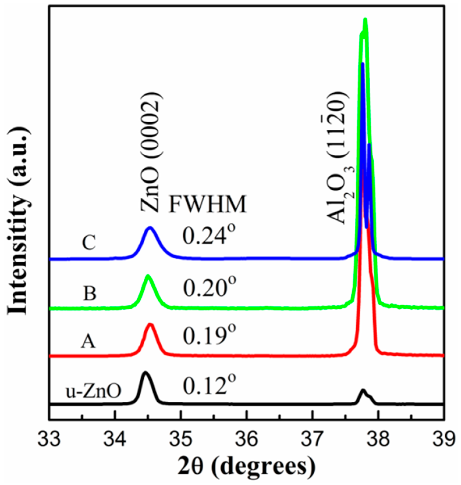
Figure 1 shows the normalized XRD spectra for all the samples. Besides the () peak from sapphire, only the (0002) peak of ZnO was observed, indicating a wurtzite structure with single c-orientation. Compared to the u-ZnO, the ZnO:N thin films show a broadening (0002) peak, and a decreasing intensity ratio of ZnO(0002)/Al2O3() with changing growth ambience from oxygen-radical-richness to oxygen-radical-deficiency. This degradation of crystal quality suggests increasing defects in the thin films, including intrinsic defects and doped N-related ones. [12,13,14]. It is noticeable that the crystalline feature was also reflected on the transparency of the four samples. The transparency of the samples falls obviously to the naked eye by the changing of the growth ambience.
The electrical properties of the films were analyzed in four-probe van der Pauw configuration on an HMS7707 Hall measurement system. Indium spot electrodes were made at the four corners of a square sample (5 × 5 mm2), and Ohmic contact of the electrodes was confirmed. The results are summarized in Table 1. The typical thicknesses of the ZnO:N thin films are about 800 nm, which was measured by a profilometer (Dektak XT). It was found that the conduction type conversed gradually when the ambience was changed from oxygen-rich, verified by the growth rate dependent on Zn source temperature, to oxygen-deficient accompanied with the increase of the N/O ratio. This is ascribed to the compensation of native donors by the doped N acceptors. Due to the larger electronegativity (3.50) of the oxygen atom than the nitrogen atom (3.04), [15] Zn atoms prefer to bond with O atoms, especially in the case of high NO flux, i.e. oxygen-rich ambience. So, the conductivity is still n-type due to the low nitrogen doping level. With an increasing N2/NO flux ratio, the N/O atom ratio was also elevated. It resulted in the increase of nitrogen doping level. Sample B exhibited p-type conduction with a hole concentration of 3.27 × 1016 cm−3, and a carrier mobility of 0.31 cm2·V−1·s−1. Such a low hole mobility is a common phenomenon in ZnO:N, which has been ascribed to the poor crystal quality suggested by XRD, owing to a heavy doping effect. [16] By further increasing the N2/NO flux ratio, the thin film should have shown better p-type properties. However, sample C began to show an indefinite type of conductivity with high resistance, which mixed n- and p-type behavior. We speculate it originates from strong compensation by donor-like defects formed in the oxygen-deficient ambience.
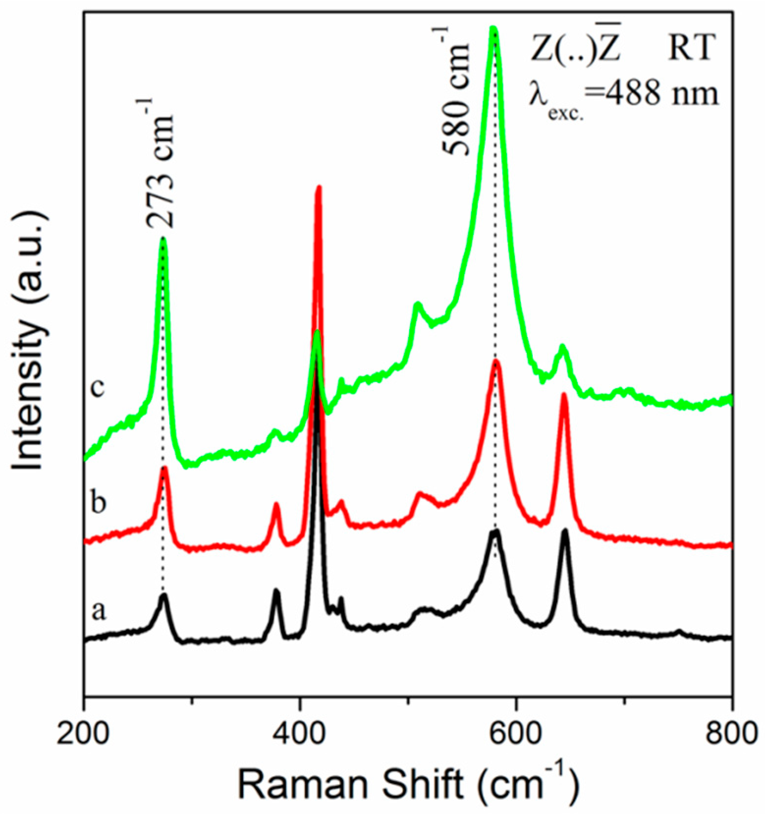
Raman scattering is a powerful nondestructive technique for studying crystalline quality, structural disorder, and defects in doped semiconductors. The influence of nitrogen doping can be reflected on the Raman spectra. Figure 2 shows the normalized Raman backscattering spectra of samples A, B and C. The 378, 419, 577, 647 and 753 cm−1 peaks are from the sapphire substrate. The laser power of 50 mW and the scan times of 10 were used.
The peaks at 437 and 580 cm−1 correspond to E2(high) and A1(LO) + E1(LO) modes of ZnO [17] respectively. An anomalous vibration mode at 273 cm−1 was also observed in the spectra. This mode was usually regarded as a wurtzite-ZnO silent mode, aroused by the breakdown of translational crystal symmetry induced by defects and impurities. [18] Therefore, the sharpening of the 273 cm−1 Raman peak with the increase of the flux ratio of N2/NO reflects the enhancement of doping level by hetero-atoms to a certain degree.
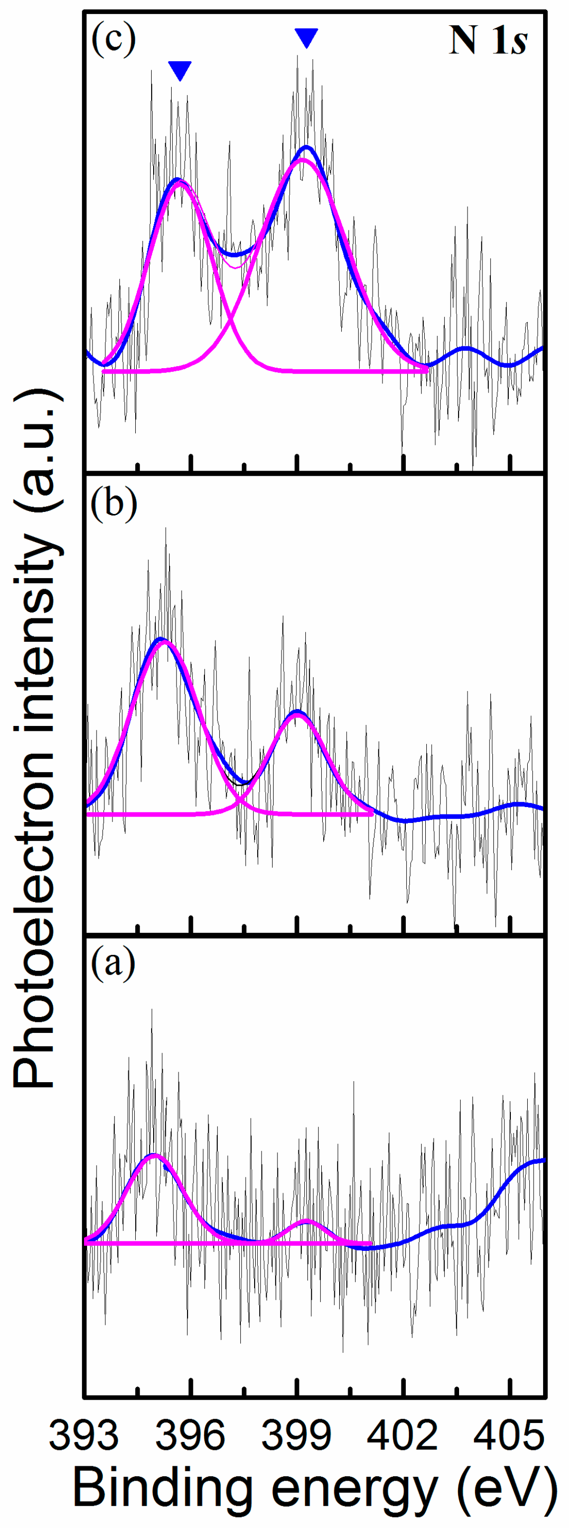
To investigate the evolution of N content and electric states, N1s XPS spectra for the three ZnO:N thin films were measured, as shown in Fig. 3. Before the measurements, the samples were etched by Ar+ for 1 min to get rid of surface contaminants. Then the scan time of 100 was used to achieve a high resolution. The binding energy (BE eV) was corrected with the C 1s (284.6 eV) as standard. For the three N-doped ZnO samples, peaks at 395.5 and 403.8 eV always appeared in the XPS spectra, which were considered to be from NO [19] and N2(O) [20], respectively. It is obvious that the N1s peak of NO increased gradually with the enhancing of the zinc-rich ambience. The peak located at 399.2 eV can be assigned to CN bonds. [21] The CN molecule will occupy an oxygen site easily, because of lower formation energy in ZnO, defined as CN(O), which has been reported in many literatures. [22] It is interesting that the signal intensity of NO and CN(O) was strengthened synchronously with the growth condition changing from oxygen-radical-rich to oxygen-radical-deficient ambience, as shown in Figure 3.
The total N concentration in samples A, B, and C are 0.6 × 10²⁰, 6.7 × 10²⁰, and 8.2 × 1020 cm−3, respectively, which were estimated by using the formula:
where Si(i=Zn, O or N) is the integral intensity of peak for N, Zn, and O elements, and asf is the atomic scattering factor. Since the calculation of atomic concentrations from XPS spectra is semiquantitative, the variation tendency that the N concentration increases monotonally in the sequence from sample A to C, agrees well with the Raman result. In sample C, the N concentration approaches 1021 cm−3, corresponding to about 1% atomic ratio in the ZnO matrix. However, it shows an indefinite conduction, rather than a p-type one. It means that the N-related acceptors in ZnO were passivated or compensated partially.
It is worth noting that the N2(O) peak is weakest in the three XPS N1s signals for all the three samples, reflecting that N2(O) was depressed efficiently. But, the integral area ratio of CN(O)/NO peaks increased in sequence from sample A to C. Since surface carbon contaminants have been diminished extremely by Ar+ etching, the CN(O) should exist in the ZnO thin films. The CN complex has been demonstrated as a donor-like defect with relatively low formation energy in ZnO:N, [23,24] as reported frequently in MOCVD-fabricated ZnO films. In this experiment, the heater of the sample holder is made of graphite. The cyanide-type radical may be formed through reaction between N atoms and volatiles from graphite, when RF activated N2 and NO plasma were introduced into the growth chamber. [25,26] With the N2/NO flux ratio increasing, the atmosphere was changed from oxygen-radical-rich to oxygen-radical-deficient ambience. In this case, CN(O) has lower formation energy in ZnO thin films, acting as a compensation source in sample C. That is to say, accompanied with an increase of N-related acceptor, CN complex, a strong compensation source, has also a great chance to be introduced into ZnO under oxygen-radical-deficient ambience. It is obvious that the source of carbon impurity is different from that in MOCVD growth, because there were hardly any hydrocarbon radicals in the MBE chamber. The exact formation mechanism and bonding configuration of CN(O) still need further investigation.
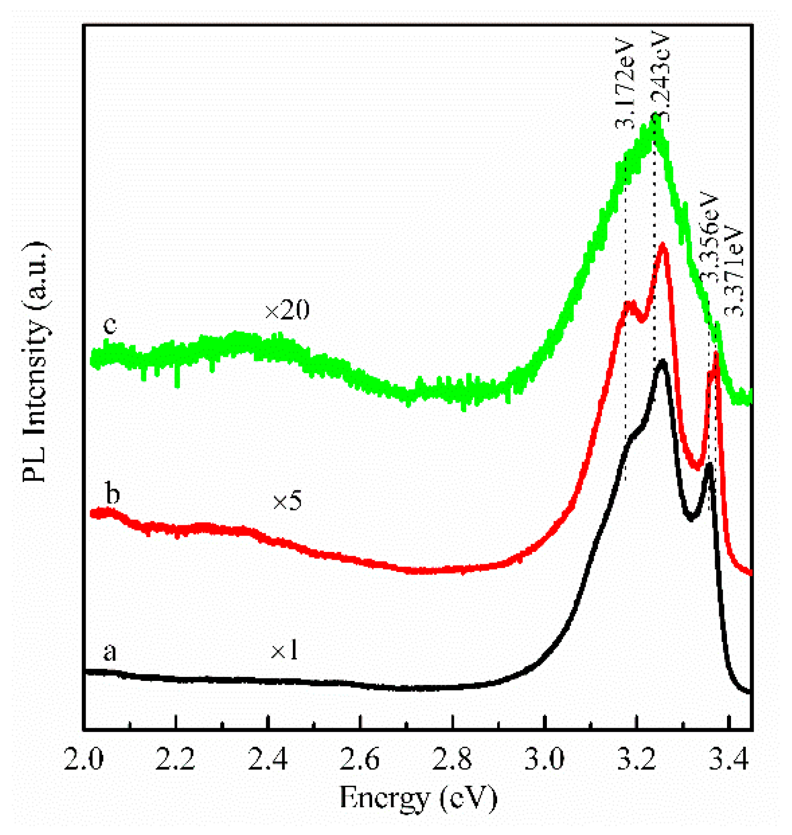
To continue to explore the change of defects in the films, low-temperature photoluminescence (PL) spectra were measured at 83 K, as shown in Figure 4. The peak located at 3.356 eV is assigned to the radiative recombination of excitons bound to a neutral acceptor (A0X). [27] The shoulder at 3.371 eV besides A0X is assigned to free exciton (FX) emission. With an increasing total nitrogen content by changing gas fluxes, the 3.243 eV peak dominates the PL band gradually.
It is assigned to donor-acceptor pair (DAP) transition. The peak at 3.172 eV is the first Longitudinal optical (LO) phonon replica of the DAP. [28] The broad green emission bands covering the region of 2.2–2.6 eV are related to single ionized O vacancy (VO+). [29,30] When the ambience converted gradually to oxygen-deficient, the green emission was enhanced synchronously. Therefore, based upon the above experiments and discussions, carbon can be easily introduced into ZnO under an O-radical-deficient condition, which ambience is often needed to increase the nitrogen doping level. It can passivate the N(O) acceptor by forming CN complex with an increase in active N atoms, and the CN complex can further compensate other N-related acceptors in ZnO.
4. Conclusions
In summary, ZnO:N thin film has been deposited on a-plane Al2O3 by P-MBE. XPS, Raman and PL measurements demonstrated a greater incorporation of N into the ZnO lattice in oxygen-radical-deficient ambience, than in an oxygen-radical-rich one. Accompanied with the N(O) incorporation, CN(O), a donor-like defect with low formation energy in ZnO:N, is confirmed to be formed in O-deficient ambience. To minimize the passivation and compensation of N-acceptor, carbon contaminant should be reduced. Otherwise, it is necessary that a compromise between the amount of oxygen and nitrogen in plasma, especially in an ambience including carbonaceous species.
Author Contributions
X.C. wrote, conceived and designed the experiments, Z.Z., B.Y. and B.L. provided resources and systems to work, Q.G. provided support in data analysis, Y.Z. supervised the work.
Funding
The authors wish to acknowledge the support of the National Natural Science Foundation of China under grant No. 61674096.
Conflicts of Interest
The authors declare no conflicts of interest.
References
- Bagnall, D.M.; Chen, Y.F.; Zhu, Z.; Yao, T.; Koyama, S.; Shen, M.Y.; Goto, T. Optically pumped lasing of ZnO at room temperature. Appl. Phys. Lett. 1997, 70, 2230–2232. [Google Scholar] [CrossRef]
- Service, R.F. Materials science—Will UV lasers beat the blues? Science 1997, 276, 895. [Google Scholar] [CrossRef]
- Norton, D.P.; Heo, Y.W.; Ivill, M.P.; Ip, K.; Pearton, S.J.; Chisholm, M.F.; Steiner, T. ZnO: Growth, doping & processing. Mater. Today 2004, 7, 34–40. [Google Scholar]
- Bian, J.M.; Li, X.M.; Gao, X.D.; Yu, W.D.; Chen, L.D. Deposition and electrical properties of N-In codoped p-type ZnO films by ultrasonic spray pyrolysis. Appl. Phys. Lett. 2004, 84, 541–543. [Google Scholar] [CrossRef]
- Tsukazaki, A.; Ohtomo, A.; Onuma, T.; Ohtani, M.; Makino, T.; Sumiya, M.; Ohtani, K.; Chichibu, S.F.; Fuke, S.; Segawa, Y.; et al. Repeated temperature modulation epitaxy for p-type doping and light-emitting diode based on ZnO. Nat. Mater. 2005, 4, 42–46. [Google Scholar] [CrossRef]
- Jiao, S.J.; Zhang, Z.Z.; Lu, Y.M.; Shen, D.Z.; Yao, B.; Zhang, J.Y.; Li, B.H.; Zhao, D.X.; Fan, X.W.; Tang, Z.K. ZnO p-n junction light-emitting diodes fabricated on sapphire substrates. Appl. Phys. Lett. 2006, 88, 031911. [Google Scholar] [CrossRef]
- Kato, H.; Yamamuro, T.; Ogawa, A.; Kyotani, C.; Sano, M. Impact of Mixture Gas Plasma of N-2 and O-2 as the N Source on ZnO-Based Ultraviolet Light-Emitting Diodes Fabricated by Molecular Beam Epitaxy. Appl. Phys. Express 2011, 4, 091105. [Google Scholar] [CrossRef]
- Lyons, J.L.; Janotti, A.; Van de Walle, C.G. Why nitrogen cannot lead to p-type conductivity in ZnO. Appl. Phys. Lett. 2009, 95, 252105. [Google Scholar] [CrossRef]
- Liu, L.; Xu, J.L.; Wang, D.D.; Jiang, M.M.; Wang, S.P.; Li, B.H.; Zhang, Z.Z.; Zhao, D.X.; Shan, C.X.; Yao, B.; et al. p-Type Conductivity in N-Doped ZnO: The Role of the N-Zn-V-O Complex. Phys. Rev. Lett. 2012, 108, 215501. [Google Scholar] [CrossRef]
- Nakahara, K.; Takasu, H.; Fons, P.; Yamada, A.; Iwata, K.; Matsubara, K.; Hunger, R.; Niki, S. Growth of N-doped and Ga plus N-codoped ZnO films by radical source molecular beam epitaxy. J. Cryst. Growth 2002, 237–239, 503–508. [Google Scholar] [CrossRef]
- Yan, Y.; Zhang, S.B.; Pantelides, S.T. Control of doping by impurity chemical potentials: Predictions for p-type ZnO. Phys. Rev. Lett. 2001, 86, 5723–5726. [Google Scholar] [CrossRef]
- Park, C.H.; Zhang, S.B.; Wei, S.H. Origin of p-type doping difficulty in ZnO: The impurity perspective. Phys. Rev. B 2002, 66, 073202. [Google Scholar] [CrossRef]
- Lee, E.C.; Kim, Y.S.; Jin, Y.G.; Chang, K.J. Compensation mechanism for N acceptors in ZnO. Phys. Rev. B 2001, 64, 085120. [Google Scholar] [CrossRef]
- Park, S.H.; Minegishi, T.; Lee, H.J.; Park, J.S.; Im, I.H.; Yao, T.; Oh, D.C.; Taishi, T.; Yonenaga, I.; Chang, J.H. Investigation of the crystallinity of N and Te codoped Zn-polar ZnO films grown by plasma-assisted molecular-beam epitaxy. J. Appl. Phys. 2010, 108, 093518. [Google Scholar] [CrossRef]
- Futsuhara, M.; Yoshioka, K.; Takai, O. Optical properties of zinc oxynitride thin films. Thin Solid Films 1998, 317, 322–325. [Google Scholar] [CrossRef]
- Singh, A.V.; Mehra, R.M.; Wakahara, A.; Yoshida, A. p-type conduction in codoped ZnO thin films. J. Appl. Phys. 2003, 93, 396–399. [Google Scholar] [CrossRef]
- Kim, Y.I.; Cadars, S.; Shayib, R.; Proffen, T.; Feigerle, C.S.; Chmelka, B.F.; Seshadri, R. Local structures of polar wurtzites Zn1−xMgxO studied by Raman and Zn-67/Mg-25 NMR spectroscopies and by total neutron scattering. Phys. Rev. B 2008, 78, 195205. [Google Scholar] [CrossRef]
- Manjón, F.J.; Marí, B.; Serrano, J.; Romero, A.H. Silent Raman modes in zinc oxide and related nitrides. J. Appl. Phys. 2005, 97, 053516. [Google Scholar] [CrossRef]
- Gao, L.L.; Yao, B.; Liu, B.; Liu, L.; Yang, T.; Liu, B.B.; Shen, D.Z. Effects of Mg concentration on solubility and chemical state of N in N-doped MgZnO alloy. J. Chem. Phys. 2010, 129, 024514. [Google Scholar] [CrossRef]
- Zhang, B.Y.; Yao, B.; Li, Y.F.; Zhang, Z.Z.; Li, B.H.; Shan, C.X.; Zhao, D.X.; Shen, D.Z. Investigation on the formation mechanism of p-type Li-N dual-doped ZnO. Appl. Phys. Lett. 2010, 97, 222101. [Google Scholar] [CrossRef]
- Yang, D.X.; Velamakanni, A.; Bozoklu, G.; Park, S.; Stoller, M.; Piner, R.D.; Stankovich, S.; Jung, I.; Field, D.A.; Ventrice, C.A., Jr.; et al. Chemical analysis of graphene oxide films after heat and chemical treatments by X-ray photoelectron and Micro-Raman spectroscopy. Carbon 2009, 47, 145–152. [Google Scholar] [CrossRef]
- Perkins, C.L.; Lee, S.H.; Li, X.N.; Asher, S.E.; Coutts, T.J. Identification of nitrogen chemical states in N-doped ZnO via X-ray photoelectron spectroscopy. J. Appl. Phys. 2005, 97, 034907. [Google Scholar] [CrossRef]
- Look, D.C.; Hemsky, J.W.; Sizelove, J.R. Residual native shallow donor in ZnO. Phys. Rev. Lett. 1999, 82, 2552–2555. [Google Scholar] [CrossRef]
- Limpijumnong, S.; Li, X.N.; Wei, S.H.; Zhang, S.B. Substitutional diatomic molecules NO, NC, CO, N-2, and O-2: Their vibrational frequencies and effects on p doping of ZnO. Appl. Phys. Lett. 2005, 86, 151910. [Google Scholar] [CrossRef]
- Taylor, J.A.; Gerald, M.L.; Rabalais, J.W. Interactions of N2+ and NO+ ions with surfaces of graphite, diamond, teflon, and graphite monofluoride. J. Am. Chem. Soc. 1978, 100, 4441–4447. [Google Scholar] [CrossRef]
- Polo, M.C.; Aguiar, R.; Serra, P.; Clèries, L.; Varela, M.; Esteve, J. Carbon nitride thin films obtained by laser ablation of graphite in a nitrogen plasma. Appl. Surf. Sci. 1996, 96–98, 870–873. [Google Scholar] [CrossRef]
- Ding, M.; Zhao, D.X.; Yao, B.; Li, B.H.; Zhang, Z.Z.; Shen, D.Z. The p-type ZnO film realized by a hydrothermal treatment method. Appl. Phys. Lett. 2011, 98, 062102. [Google Scholar] [CrossRef]
- Sans, J.A.; Segura, A.; Mollar, M.; Marí, B. Optical properties of thin films of ZnO prepared by pulsed laser deposition. Thin Solid Films 2004, 453–454, 251–255. [Google Scholar] [CrossRef]
- Yao, B.; Shen, D.Z.; Zhang, Z.Z.; Wang, X.H.; Wei, Z.P.; Li, B.H.; Lv, Y.M.; Fan, X.W. Effects of nitrogen doping and illumination on lattice constants and conductivity behavior of zinc oxide grown by magnetron sputtering. J. Appl. Phys. 2006, 99, 123510. [Google Scholar] [CrossRef]
- Ahn, C.H.; Kim, Y.Y.; Kim, D.C.; Mohanta, S.K.; Choa, H.K. A comparative analysis of deep level emission in ZnO layers deposited by various methods. J. Appl. Phys. 2009, 105, 013502. [Google Scholar] [CrossRef]
Figure 1.
The XRD patterns of the undoped zinc oxide (ZnO), and ZnO:N films grown under (A) FNO = 0.8, FN2 = 0.4, (B) FNO = 0.6, FN2 = 0.6 and (C) FNO = 0.4, FN2 = 0.8 (SCCM).
Figure 1.
The XRD patterns of the undoped zinc oxide (ZnO), and ZnO:N films grown under (A) FNO = 0.8, FN2 = 0.4, (B) FNO = 0.6, FN2 = 0.6 and (C) FNO = 0.4, FN2 = 0.8 (SCCM).

Figure 2.
Room temperature Raman backscattering spectra for samples (a) A, (b) B, and (c) C.

Figure 3.
N 1s XPS spectra for the samples (a) A, (b) B, and (c) C, respectively.

Figure 4.
PL spectra of the samples (a) A, (b) B, and (c) C at 83 K.


Table 1.
Electrical properties and nitrogen concentration of undoped ZnO and ZnO:N films with different NO and N2 flux.
Table 1.
Electrical properties and nitrogen concentration of undoped ZnO and ZnO:N films with different NO and N2 flux.
| Sample | FNO (SCCM) | FN2 (SCCM) | [N] (cm−3) | µ (cm2 /V s) | nc (cm−3) | Resistivity (Ω cm) | Carriers Type |
|---|---|---|---|---|---|---|---|
| u-ZnO | … | … | … | 25 | ~1018 | 0.2 | n |
| A | 0.8 | 0.4 | 0.6 × 10²⁰ | 1.84 | 6.35 × 10¹⁷ | 6 | n |
| B | 0.6 | 0.6 | 6.7 × 10²⁰ | 0.31 | 3.27 × 10¹⁶ | 868 | p |
| C | 0.4 | 0.8 | 8.2 × 10²⁰ | … | … | 11800 | indefinite |
© 2019 by the authors. Licensee MDPI, Basel, Switzerland. This article is an open access article distributed under the terms and conditions of the Creative Commons Attribution (CC BY) license (http://creativecommons.org/licenses/by/4.0/).
Share and Cite
MDPI and ACS Style
Chen, X.; Zhang, Z.; Zhang, Y.; Yao, B.; Li, B.; Gong, Q. Passivation Mechanism of Nitrogen in ZnO under Different Oxygen Ambience. Crystals 2019, 9, 204. https://0-doi-org.brum.beds.ac.uk/10.3390/cryst9040204
AMA Style
Chen X, Zhang Z, Zhang Y, Yao B, Li B, Gong Q. Passivation Mechanism of Nitrogen in ZnO under Different Oxygen Ambience. Crystals. 2019; 9(4):204. https://0-doi-org.brum.beds.ac.uk/10.3390/cryst9040204
Chicago/Turabian StyleChen, Xingyou, Zhenzhong Zhang, Yunyan Zhang, Bin Yao, Binghui Li, and Qian Gong. 2019. "Passivation Mechanism of Nitrogen in ZnO under Different Oxygen Ambience" Crystals 9, no. 4: 204. https://0-doi-org.brum.beds.ac.uk/10.3390/cryst9040204
Note that from the first issue of 2016, this journal uses article numbers instead of page numbers. See further details here.