Geometric Structure behind Duality and Manifestation of Self-Duality from Electrical Circuits to Metamaterials


1
Research Center for Advanced Science and Technology, The University of Tokyo, Meguro-ku, Tokyo 153-8904, Japan
2
Center for Emergent Matter Science, RIKEN, Wako, Saitama 351-0198, Japan
3
Department of Electronic Science and Engineering, Kyoto University, Kyoto 615-8510, Japan
*
Author to whom correspondence should be addressed.
†
Current address: Graduate School of Engineering Science, Osaka University, Toyonaka, Osaka 560-8531, Japan.
Symmetry 2019, 11(11), 1336; https://0-doi-org.brum.beds.ac.uk/10.3390/sym11111336
Submission received: 31 August 2019
/
Revised: 6 October 2019
/
Accepted: 14 October 2019
/
Published: 28 October 2019
(This article belongs to the Special Issue Duality Symmetry)
Abstract
:In electromagnetic systems, duality is manifested in various forms: circuit, Keller–Dykhne, electromagnetic, and Babinet dualities. These dualities have been developed individually in different research fields and frequency regimes, leading to a lack of unified perspective. In this paper, we establish a unified view of these dualities in electromagnetic systems. The underlying geometrical structures behind the dualities are elucidated by using concepts from algebraic topology and differential geometry. Moreover, we show that seemingly disparate phenomena, such as frequency-independent effective response, zero backscattering, and critical response, can be considered to be emergent phenomena of self-duality.
1. Introduction
Duality is an indispensable concept in mathematics, physics, and engineering. It relates two seemingly different systems in a nontrivial manner and facilitates deeper insight into the underlying structures behind the relevant physical theories. A duality transformation converts an object to its dual counterpart. Performing duality transformations twice brings a system back to its original state. Advantageously, duality transformation can sometimes convert a difficult problem into a more tractable one. Moreover, if a system is dual to itself, namely self-dual, some special characteristics could be expected. To name a few, self-duality characterizes a critical probability and temperature for percolation on graphs [1,2] and two-dimensional Ising models [3], respectively.
For electromagnetic systems, duality appears in various forms, such as dual circuits [4,5], Keller–Dykhne duality [6,7,8], electromagnetic duality [9,10,11], input–impedance duality for antennas [12,13], and Babinet’s principle [14,15,16,17,18,19,20,21,22,23,24,25,26]. These dualities have been individually developed in various research fields such as electrical engineering, radio-frequency engineering, and photonics because the relevant frequency spectra broadly range from direct-current to the optical regime. Despite the long history of dualities in electromagnetic systems, they have not been sufficiently discussed from a unified perspective. In particular, universal geometrical structures behind the dualities are still mathematically unclear in electromagnetic systems.
Recently, engineered artificial composites called metamaterials have been attracting much attention due to their exotic electromagnetic properties [27]. In particular, two-dimensional metamaterials are called metasurfaces and are intensively studied as ultrathin functional devices [28,29,30]. The operating frequency of metamaterials has been extended from the microwave to the optical band, and versatile design principles over extensively wide frequency spectra are in high demand. For example, circuit designs and nano-optics were integrated to establish a universal strategy to design metamaterials [31]. Over the past few decades, duality has been assuming an important role in the research and development of metamaterials. To name a few such cases, duality has been leveraged to design complementary metasurfaces [32,33,34,35], self-complementary metasurfaces [36,37,38,39,40,41,42], critical metasurfaces [43,44,45,46,47,48,49,50,51,52], maximally chiral metamaterials [53], and self-dual metamaterials with zero backscattering [54] or helicity conservation [55,56,57]. In such situations, the extensive target frequencies of metamaterials require a comprehensive understanding of duality in a unified manner.
In this paper, we establish a unified perspective which synthesizes dualities appearing in electromagnetic systems. The underlying geometrical structures hidden behind dualities are uncovered through Poincaré duality between circuit theory to optics. To this end, we introduce inner and outer orientations of geometrical objects. We stress the importance of these two different kinds of orientations because it is sometimes overlooked in primary electromagnetism. The correspondence relationship among various dualities in electromagnetic systems is thoroughly discussed. Moreover, we comprehensively show that self-duality manifests as frequency-independent effective response, zero backscattering, and criticality in electromagnetic systems. As a whole, we attempted to keep the paper pictorial as much as possible in order to easily grasp the important concepts for duality.
In Section 2, we start with discussions of electrical circuits. Although electrical circuits are simplified and idealized systems, they include the essence of duality. To clearly see duality in circuit theory, we provide an algebraic-topological framework for electrical circuits. Based on the established framework, we strictly formulate circuit duality through Poincaré duality. Furthermore, we explain that the effective response of a self-dual circuit is automatically derived from its self-duality. In Section 3, we discuss zero backscattering for waves in self-dual circuits in terms of impedance matching. Section 4 generalizes circuit duality to Keller–Dykhne duality for a continuous two-dimensional resistive sheet. We show that critical behavior can appear for a self-dual sheet. To extract the essence of the duality in continuous systems, differential forms are utilized. We see that Keller–Dyhkne duality exactly corresponds to circuit duality through discretization. In Section 5, we introduce electromagnetic duality to Maxwell’s electromagnetic theory. Electromagnetic duality in a four-dimensional spacetime has a similar structure to Keller–Dykhne duality in a two-dimensional plane. Section 6 introduces duality for wave radiation and scattering by a two-dimensional sheet. Combining electromagnetic duality and mirror symmetry of the sheet, we establish Babinet duality. Babinet duality induces the critical response of a metallic checkerboard-like sheet. Finally, Section 7 summarizes the unified perspective for dualities appearing in electromagnetic systems and gives a conclusion.
2. Circuit Theory
In this section, we establish a comprehensive formulation of circuit theory based on algebraic topology. Within the proposed framework that makes use of Poincaré duality, we unveil the geometrical structure of circuit duality. Next, we discuss the resultant duality in effective response and show that a specific response is automatically guaranteed under self-duality. Compared to the previous algebraic topological formulation of the circuit theory [58,59,60], we clarify the importance of inner and outer orientations of geometrical objects for circuit duality. Our approach gives a succinct mathematical description of circuit duality, and an amalgamation of circuit theory and algebraic topology yields various benefits in this interdisciplinary area.
2.1. Duality between Current and Voltage
■ Circuits as Graphs
A circuit is considered as a network of interconnected components. The interconnection relation can be represented by a graph with a set expressing the totality of nodes and a set representing the totality of directed edges (an ordered 2-element subset of ), where is the number of elements of a set . Elements in and are called 0- and 1-cells, respectively. Circuit elements such as voltage sources or resistors are placed along the graph edges. In this section, we mainly focus on circuits with resistors, voltage, and current sources. Figure 1 shows an example of a circuit and the corresponding graph.
■ Chains
Consider a current distribution with flowing along each edge . Here, is directed and flows in the direction of . A negative represents a current flow in the reverse direction of . This current distribution can be represented by a formal sum , where generates a vector space over real numbers . In a strict sense, we should consider with the unit of ampere instead of for a current distribution, but we omitted the unit to avoid notation complexity. A vector spanned by elements in is called a 1-chain. The vector space composed of all 1-chains is denoted by . Similarly, we can define a 0-chain as with , and introduce a vector space over as the totality of 0-chains.
■ Boundary Operator
Now, we extract the connection information regarding . Consider an edge e directing from a node to . As shown in Figure 2, the boundary of e is given by . Extending the definition linearly, we can introduce a linear boundary operator . The matrix representation of ∂ is denoted by , called the incidence matrix. For the previous example in Figure 1b, we obtain the following matrix representation of ∂:
with
■ Kirchhoff’s Current Law
To understand the physical meaning of ∂, we consider for a current distribution . The coefficient of for represents the net inflow of the current: the current inflow to n minus the current outflow from n. Therefore, the boundary operator can be used to express Kirchhoff’s current law (KCL), which states that net current inflows at each node are zero. KCL restricts current distribution to a linear subspace . For Equation (2), we have , and from the rank–nullity theorem [61]. The basis of is given by . Here, and are closed loops called meshes. Generally, we can construct a basis of with meshes [60].
■ Cochains
Next, we represent a voltage distribution in geometric terms. For a finite-dimensional vector space U, we can define its dual space , where is a linear map and is a vector space with . An element can be interpreted as an apparatus which measures a vector and yields . For a basis in U, we can define a dual basis in satisfying , where the Kronecker delta is 1 if ; otherwise, 0. For a vector with , extracts the component with respect to as .
Along an edge, we can calculate power consumption as a real scalar equal to the voltage multiplied by the current. The total power consumption in the circuit is the sum of power consumption over all edges (power generation is represented by negative power consumption). Therefore, a voltage distribution is considered as yielding total power for . An element in is called a 1-cochain. In , we have a dual basis . Then, we can express for and . We also write as to stress the analogy to the theory of continuous fields. A 0-cochain also acts for a 0-chain as .
■ Kirchhoff’s Voltage Law
Now, we reframe Kirchhoff’s voltage law (KVL) in our geometric approach. KVL states that the sum of voltages along any loop must be zero. Then, a voltage distribution must satisfy for all (also known as Tellegen’s theorem) because I is generated from mesh currents. To concisely express KVL, we define a null space for a linear subspace in U as The dimension of the null space is given by . The relation between and is schematically depicted in Figure 3. By using the concept of a null space, KVL is clearly rewritten to restrict voltage distribution to .
■ Dual Operators
Next, we want to define a dual boundary operator for ∂. Let U and W be finite-dimensional vector spaces, and consider a linear map . Then, a dual map is defined as for and all . Let and be the bases of U and W, respectively. We have with the matrix representation of f as . This shows that the matrix representation of the dual map is the transpose of the matrix representation of the original map. Using the concept of the dual map, we can define a coboundary operator to satisfy for all and . For a dual basis obtained from 0-cells , we have with the incidence matrix . For the example of Figure 1b, we have
■ Potential and Kirchhoff’s Voltage Law
Finally, we discuss a relation between KVL and a potential. KVL was formulated to state that the voltage drop along any loop is zero, but how is this statement related to the existence of a potential? To see this, we start from a general statement. Consider a linear map . The image and kernel of linear maps f and are related through and [61]. The proof of the first statement is as follows. First, holds because we have for all with . Second, holds due to the rank–nullity theorem. Then, we obtain . A similar proof is applied for the second statement. Now, we come back to circuit theory and define . From , we obtain . This means that there is a potential which satisfies for a voltage distribution V.
■ Summary of Circuit Equations
The discussions so far show the duality between KCL and KVL. These results are summarized in Figure 4. Importantly, the degree of freedom for currents and voltages constrained by KCL and KVL is given by . On the other hand, a circuit element along each edge gives the relation between the current and voltage on the edges, and we have equations with respect to all the circuit elements. Therefore, the current and voltage distributions are unambiguously determined.
2.2. Planar Graph as Cellular Paving
Consider the series and parallel resistors shown in Figure 5. Series resistors and have the composite resistance . On the other hand, parallel resistors and have the total resistance , satisfying . We can clearly see the duality between resistance and conductance (given by an inverse relationship) for series and parallel resistances. This duality universally holds in more general situations, as we show in Section 2.5. In this subsection, we set up a fundamental geometric structure to establish circuit duality.
■ 2-Chains in Planar Graphs
The graph shown in Figure 1b is planar, i.e., its edges intersect only at their nodes. For a planar graph, we can define faces. In Figure 6, we show directed faces , where the internal direction of each face is represented by the directed circle. Elements of are called 2-cells. Note that we include the unbounded face outside the circuit. The area of face can be finite if we consider the planar graph to be on a sphere. The vector space generated by is denoted by . It is natural to define a boundary operator , such that [] if is included in f in the same [opposite] direction; otherwise, . For Figure 6, we have
Note that holds, i.e., the boundary of a cell boundary is empty.
■ Cellular Paving
In the previous examples, cells fully paved the two-dimensional plane without any gap. Such a paving is often called a mesh in finite element analysis. Naturally, a p-cell is defined as a p-dimensional directed face, which is extended from a 0-cell (point), 1-cell (edge), and 2-cell (face). Cellular paving with the cells can be rigorously formulated in higher-dimensional spaces. The boundary of each element is represented by a combination of lower-dimensional cells. Strictly speaking, a cellular paving of some region R in a manifold is a finite set of open directed p-cells such that (i) two distinct cells do not intersect, (ii) the union of all cells is R, and (iii) if the closures of two cells c and meet, their intersection is the closure of a unique cell [62]. However, we only need to grasp the concept of cellular paving with an intuitive sense.
For a cellular paving in an m-dimensional region, we can define generated from i-cells with a boundary operator satisfying . Following a similar treatment for graphs, and are defined. Next, we consider a dual space . As dual counterparts of and , we can define and . To extract topological characteristics, homology and cohomology groups are defined as and , respectively. It is known that and do not depend on specific cellular paving, but only on the original m-dimensional region.
2.3. Inner and Outer Orientations
■ Intuitive Explanation of Inner and Outer Orientations
Thus far, cells were assumed to be (internally) oriented. In this subsection, we clarify the definition of orientation and provide a deeper explanation that is crucial for understanding the circuit duality. First, one can intuitively grasp two types of orientation defined for a surface in a three-dimensional space. In Figure 7a, the surface is internally oriented, where “internally” means that the orientation is defined through the internal coordinates of the surface, regardless of whether or not the surface is embedded in the three-dimensional space. On the other hand, we could consider an outer orientation of the surface as the normal-vector field as shown in Figure 7b. Outer orientation refers to the transverse direction of the surface and involves ambient space. To discuss how much fluid traverses the surface, we do not use an inner-oriented surface, but an outer-oriented one. These two types of orientation are strictly defined below and are important to express various physical quantities.
■ Inner Orientation of Vector Space and Cell
As a starting point, we define an inner orientation of a vector space U. Consider two ordered bases and in U. A basis transformation is represented by . When , the direction associated with is considered to be the same as that with ; otherwise, their directions are different. Then, bases are classified as two different equivalence classes. We can choose one specific class to be positive orientation. If a vector space U has such a positive orientation, U is called inner-oriented. Generally, a tangent space is a p-dimensional vector space composed of tangent vectors at a point P on a p-dimensional surface (manifold) (Figure 8a). If tangent spaces on a p-cell are continuously oriented, it is called inner-oriented. See a schematic picture shown in Figure 8b.
■ Outer Orientation of Vector Space and Cell
Next, we introduce an outer orientation. Consider a linear subspace W in a vector space U. When we choose an orientation of the quotient vector space , we say that W is outer-oriented. The outer orientation is naturally extended to a p-cell S in an m-dimensional manifold M. Here, M is a total space including S and called ambient space. Because of , we can consider as a vector space whose (nonzero) elements are considered to be transverse to . If a p-cell has continuous orientation of for all , the cell is called outer-oriented. An example of an outer-oriented 2-cell is shown in Figure 9.
For a planar paving, we summarize all types of cells in Figure 10. An outer-oriented 0-cell is best suited to represent a rotation around a point in the two-dimensional plane. Fluid flow transverse to an edge is also represented by an outer-oriented 1-cell.
■ Inner-Orientation Representation for Outer Orientation
Outer orientation can be represented by two inner orientations depending on the orientation of ambient space. Let us see this representation in an example in a two-dimensional plane. Consider an outer-oriented edge in a planar graph. With a given orientation of the plane (two-dimensional Euclid space ), we can convert the outer orientation into an inner one as shown in Figure 11. The inner orientation is induced by rotating the outer orientation by , where the rotational direction is determined by the ambient-space orientation. Importantly, the inner direction is reversed when we choose the opposite ambient-space orientation. Thus, an outer-oriented cell can be represented by two different inner-oriented cells as with . The above intuitive discussion can be generalized in other dimensional spaces as shown in Appendix A.
■ Outer-Orientation Representation for Inner Orientation
The previous discussions on orientations are based on representations of an outer-oriented cell by inner-oriented cells. We would like to remark on a dual perspective: an inner-oriented cell can be represented by outer-oriented cells. This perspective is indicated in Figure 12. To obtain an outer orientation, the inner orientation of the edge is rotated by 90 in the reverse direction of a given orientation of the plane.
■ Operation for Outer-Oriented Chains and Cochains
Next, consider a cellular paving with outer-oriented cells. We can define a vector space generated from p-cells in . Using the representation of an outer-oriented cell by inner-oriented cells, we can define so that ∂ individually acts for each inner-oriented component. For example, an inner-oriented component of the boundary of an outer-oriented 1-cell in a plane is depicted in Figure 13. The boundary operations for outer-oriented cells in a two-dimensional plane are summarized in Figure 14.
As a dual counterpart of , the dual space is defined by applying the general theory for linear spaces. An outer-oriented cochain in is also represented by two inner-oriented cochains and the coboundary operator for outer-oriented cochains is naturally defined.
2.4. Essence of Poincaré Duality
■ Dual Paving
For a cellular paving with inner-oriented cells, we can compose a dual cellular paving with outer-oriented cells. Here, we focus on ambient space of a two-dimensional plane to introduce the concept. As shown in Figure 15a, each face in is converted to an outer-oriented point in . Each edge in is also replaced with an outer-oriented edge in transverse to the original edge. The obtained edge is connected to a point in , if the original edge is included in the original face. Furthermore, each point in is converted to a face in as shown in Figure 15b. The face is adjacent to an edge in , if the original point is connected to the original edge. Under this composition, the orientation of each cell is naturally inherited from the original cell to the dual cell.
Let us explicitly see this composition in the previous example, where the original cellular paving is shown again in Figure 16a. By applying the above procedure for shown in Figure 16a, we obtain the dual paving as shown in Figure 16b.
■ Poincaré Duality
For this dual paving, we have the following matrix representations of ∂:
2.5. Dual Circuits
■ Poincaré Duality and Circuit Duality
Now, let us introduce dual circuits. Consider a circuit on a planar graph. The planar graph is seen as a cellular paving for a two-dimensional plane (or a sphere surface). Because there is no nontrivial loop on a plane or sphere, we have the following equation:
Let and be current and voltage distributions satisfying KCL and KVL, respectively. We set a reference resistance to exchange a current and voltage. Consider current and voltage distributions for a circuit on , where and are defined with . Note that and are outer-oriented, but we can obtain an inner-oriented component for a given orientation of the plane. By combining Equation (9) with Equation (11), KCL and KVL are shown to hold for and as explained below. Here, we check KVL for . From Equation (11), a current distribution can be written as with “face” (or mesh) currents . Then, we have , which indicates . A similar discussion to KCL holds for .
A current and voltage relation along a circuit element located at each edge is written by for , and . As a dual relation, we define . If we assign a circuit element with for each edge in , and give a solution of the circuit on . For example, consider a resistance with Ohm’s law with scalar V, I, and R. Substituting , , we have with . Importantly, we obtain
for . The derived circuit on is called a dual circuit. The dual relation is summarized in Table 1.
For the previous example shown in Figure 17a, we construct a dual circuit as shown in Figure 17b. Here, we have , , and take a specific orientation (⥀) of the plane to obtain an inner orientation of the current source. We can clearly see the duality between series and parallel connections in Figure 17. Therefore, the concept of dual circuits is considered as a generalization of series–parallel duality.
■ Duality for Composite Resistances
Consider a one-port network N composed of resistors. A voltage source is attached to N as shown in Figure 18a. The network N is characterized by an equivalent resistance , where and are the voltage and current along the source, respectively. Consider the dual counterpart as shown in Figure 18b. The dual network is characterized by with the current and voltage along the source. From the corresponding duality, we have
where is the reference resistance.
2.6. Self-Dual Circuit
If the self-dual relation holds for a one-port network N, the composite resistance satisfies . In this case, we obtain without solving circuit equations. As an example, we consider a bridge circuit shown in Figure 19a and its dual counterpart over is given in Figure 19b. The self-dual condition is written as . Under the self-dual condition, the circuit behaves as an effective resistor with .
Thus far, we only consider circuits with resistors, but the extension to alternating-current (AC) circuits is obvious. Under this extension, the real-number field () is replaced with the complex one (). In AC circuits, resistances are replaced with complex impedances. Consider the example of an AC circuit shown in Figure 19c. This circuit is obtained from Figure 19a by replacing , , where is an angular frequency. The self-dual condition is given by . Under the self-duality, the circuit surprisingly behaves as a frequency-independent resistor with , although capacitors and inductors exhibit frequency-dependent response. This result can be interpreted to mean that the frequency dependency of capacitors and inductors negate each other when the whole system is self-dual. Therefore, self-dual circuits provide a powerful way to produce constant-resistance circuits [64].
3. Zero Backscattering from Self-Duality
Signals can propagate in a uniform transmission line without backscattering. In this section, we associate self-duality with the zero-backscattering condition. Furthermore, we show that a large phase shift without backscattering in Huygens’ metasurfaces can be understood by using a self-dual circuit model.
3.1. Self-Dual Transmission Lines
In this section, we consider signal propagation in a transmission line, which can be expressed by an LC ladder network [65]. In contrast to previous research on duality in transmission lines [66], we provide a circuit theoretical interpretation of the characteristic impedance of a transmission line in terms of self-dual response described in Section 2.
■ Telegraph Equations
A coaxial cable, which is composed of an inner conductor as a signal line and an outer conductor as a ground shield, forms capacitors between two conductors and inductors with a magnetic field around the inner conductor as shown in Figure 20a. With inductance and capacitance per unit length, the system is discretized as the LC ladder composed of and in a unit length as shown in Figure 20b. In the i-th segment, Kirchhoff’s voltage and current laws are, respectively, expressed as
In the continuum limit of , the above equations become
which are well known as the telegraph equations. Generally, and can depend on z.
■ Zero Backscattering in Self-Dual Transmission Lines
Here, we see that the self-dual transmission line does not cause backscattering. If a transmission line has a constant impedance independent of z, then the transmission line becomes self-dual: the telegraph equations with a uniform Z are invariant under duality transformation with . In terms of the new variables , the self-dual telegraph equations are written as
where . With arbitrary functions , the general expression of the solution can be provided by , which corresponds to a propagating wave with velocity without backscatterng. If depends on z, self-duality is broken and backscattering may be observed.
■ Circuit-Theoretical Derivation of Zero Backscattering
Next, we give a circuit-theoretical derivation of zero backscattering for a self-dual system. A transmission line composed of LC ladder circuits is shown in Figure 21a, where inductances and capacitances may depend on the position i. The dual circuit with respect to a global resistance is illustrated as shown in Figure 21b. The transformed circuit elements are given as
In the limit of small and , each capacitance can be shifted to next position because the potential difference across each inductance is negligibly small. By repeating the shift of the capacitances in the original circuit as shown in Figure 21c, we obtain the same circuit as Figure 21b ( and ) under the following condition for any i:
In other words, the LC ladder network with constant is self-dual for impedance inversion with respect to defined by Equation (20). In this way, the global parameter is linked with the local impedance , which is defined by and in each site.
Next, we consider excitation of the self-dual LC ladder by a voltage source V connected at the left-hand side as shown in Figure 21d. The dual circuit is illustrated in Figure 21e, where the current source is given by . By repeating the shift of the capacitances as depicted in Figure 21f, Figure 21e can be identified with Figure 21f. As discussed in Section 2.6, the self-dual circuit is characterized by the effective resistance as shown in Figure 21g. Imagine that we connect a uniform transmission line (T1) with a characteristic impedance of to the half-infinite circuit (T2). When the signal propagates from T1 to T2, any backscattering does not appear due to the impedance matching.
■ Heaviside Condition
Self-duality can be realized in transmission lines with inductance , capacitance , conductance , and resistance as shown in Figure 22. The self-dual condition is given by
This self-dual condition is nothing but a no-distortion signal transmission condition derived by Heaviside [67]. Due to the self-duality, frequency-independent response is realized and backscattering vanishes, while a signal decays as it propagates.
3.2. Circuit Model for Huygens’ Metasurface
Two-dimensional artificial structures called metasurfaces have been extensively investigated for controlling the amplitude and phase of transmitted and/or reflected electromagnetic waves [68]. The wavefront control of light can be realized by designing metasurfaces with spatial variations of phase responses [69,70,71,72]. The amplitude and phase responses of metasurfaces are generally interdependent. Nevertheless, it is possible to control the phase of the transmitted light with constant power transmission, which could be 100% in ideal conditions without losses, by carefully designing the resonant components of the metasurfaces. Metasurfaces for the arbitrary control of transmission properties, or amplitude and phase control, are called Huygens’ metasurfaces, which have been introduced by Pfeiffer and Grbic [73]. In this subsection, we clarify the role of self-duality in Huygens’ metasurfaces.
■ Transmission and Reflection for Huygens’ Metasurfaces
It is assumed that monochromatic plane electromagnetic waves with a specific polarization are normally incident on an isotropic metasurface placed at in a vacuum with a wave impedance of . In this paper, the variable with a tilde represents the complex amplitude of a harmonically oscillating quantity , where denotes the complex conjugate of the preceding term. The complex amplitudes of macroscopic electric and magnetic fields, which are averaged over the typical scale of metasurface elements, are represented by and ( and ) for the input (output) side () in the proximity to the surface. Although electric and magnetic fields are represented by vectors, we here focus on scalar amplitudes for a specific polarization. Electromagnetic response of the metasurface is characterized by two parameters: electric sheet admittance and magnetic sheet impedance . The averaged electric fields induce surface currents , which demand the boundary condition on [74]. In the same way, the magnetic counterpart can be considered, and the averaged magnetic fields produce surface magnetic currents , which require the boundary condition . The boundary conditions are summarized as
For the incident wave propagating in the direction with the electric field and the magnetic field , the total electric and magnetic fields (, ) are represented as ( in and in , where and are the amplitude transmission and reflection coefficients. By substituting these fields at the metasurface () into Equations (22) and (23), the amplitude transmission and reflection coefficients are obtained as
where and . Hence, the reflection vanishes for . In addition to the no-reflection condition, if and are purely imaginary impedances, which are expressed as with a dimensionless number , the transmission coefficient can be written as
The incident waves are perfectly transmitted through the metasurface due to the fact that for any b, and the transmitted waves acquire a phase of . Such metasurfaces, which are typical examples of Huygens’ metasurfaces, realize arbitrary phase shift without losses in an ideal case by tailoring the design of the metasurface structures. Both of the electric and magnetic responses are indispensable for the no-reflection condition.
■ Circuit Model for Huygens’ Metasurfaces
The propagation of electromagnetic waves in a vacuum can be modeled as signal propagation in a transmission line with the wave impedance , and the metasurface is represented by circuit elements inserted in the transmission line as shown in Figure 23a. In this model, the electric field and magnetic field are replaced with voltage and current , respectively; therefore, the circuit model of the metasurface should satisfy the following conditions:
A circuit called a lattice circuit as shown in Figure 23b satisfies the above conditions [75]. The electric and magnetic responses are represented by impedances and , respectively. Equations (26) and (27) can be confirmed separately for Figure 23b, considering excitation by waves from both sides of the metasurface. For in-phase excitation , all currents are sunk into the bridge circuit, and the currents become antiphase . There is no voltage across , and the currents flow only in . Hence, we obtain , which is identical to Equation (26) for and . In the opposite case, and , the currents flow only in , and , so the equation that corresponds to Equation (27) can be derived.
■ Zero Backscattering Due to Self-Duality
For Figure 23a, provides the input impedance for the metasurface, or lattice circuit, followed by the transmission line in . The uniform semi-infinite transmission line in can be regarded as a resistor with an impedance of as shown in Figure 21g. As a result, the total system viewed from the input side is well described by a bridge circuit as shown in Figure 23c, and is identical to the impedance of the bridge circuit. As described in Section 2.6, the bridge circuit satisfying is self-dual for the inversion center , and the input impedance is always . The reflection vanishes under this condition, where the wave impedance is impedance-matched to the load represented by the bridge circuit. As a result, all energy is transmitted to the transmission line in . Thus, the no-reflection condition for Huygens’ metasurfaces is interpreted in terms of self-duality.
4. Keller–Dykhne Duality
Circuit duality can be extended for a continuous system. As with circuits, the effective response of a continuous system is associated with that of the dual one; thus, a self-dual response is automatically guaranteed. Such a constraint can induce critical behaviors of self-dual systems. Here, these topics are reviewed. Next, we introduce differential forms to clearly extract the structure of the duality in a continuous system. The correspondence between the dualities in continuous and discrete systems is formulated through discretization of continuous fields. In this section, we always use the right-hand vector product, in other words, A, B, and obey the right-hand rule.
4.1. Two-Dimensional Resistive Sheets
Consider an electric field and current density on a two-dimensional resistive sheet located at with a sheet conductance . Here, we assume that the fields inside the thin sheet are uniform along z and omit z-dependency for the fields. Thus, we treat the fields as two-dimensional vector fields independent of z. An example configuration is shown in Figure 24a. The physical dimensions of E, K, and G are V/m, A/m, and 1/, respectively. From KVL and KCL, we obtain
Note that these equations can be directly obtained from Maxwell’s equations; by omitting the time-derivative terms for steady states, we can obtain Equations (28) and (29) from Faraday’s law and the law of charge conservation. Ohm’s law is given by
where G is a conductance and generally a matrix. For a metallic electrode, the boundary condition is written as
where n is the unit vector normal to the boundary. For an open boundary, the boundary condition is given by
From Equation (28), the electric field is represented by
with a potential . Combining Equation (33) with Equations (29) and (30), we obtain
The boundary of the i-th electrode is specified by the Dirichlet boundary condition
which is constant along the boundary. The open boundary is given by the Neumann boundary condition
4.2. Duality in Laplace Equation
In this subsection, we discuss duality in Laplace equations [76]. The solution of the Laplace equation is called a harmonic function. A harmonic function can be considered as a part of a holomorphic function. To see this fact, consider a holomorphic function with , , and . The holomorphism leads to the Cauchy–Riemann equations:
These equations can be expressed as
with , which induces counterclockwise rotation. As we differentiate Equations (38) and (39) along x and y, respectively, and combine the results, we obtain
which states that u is harmonic. Similarly, v is also harmonic. Here, v is called a harmonic conjugate of u.
If u is given, how can we obtain its harmonic conjugate v? Focusing on with Equation (40), we have
where and is a fixed point. We have assumed that the considered region is simply connected to define Equation (42). When we consider a small displacement along a line , we have , which leads to . Therefore, u and v constitute an orthogonal coordinate around the point , as shown in Figure 25a. In this subsection, the operation of taking the harmonic conjugate is treated as a duality transformation.
The above result induces duality for the potential problem of the Laplace equation. Let be the harmonic conjugate of a harmonic potential . The relation between and is depicted in Figure 25b,c. Now, we come back to resistive sheet problems. The current stream lines and isopotential contours are replaced with each other under the harmonic conjugate as shown in the simplest example of Figure 26. Furthermore, we can see that the harmonic conjugate interchanges the Dirichlet and the Neumann boundary conditions because of the rotation.
4.3. Generalized Duality
Harmonic duality can be extended to a two-dimensional resistive sheet with a spatially inhomogeneous sheet conductance . Keller proved the duality for a system composed of two different conductances [6], and Dykhne generalized it to a system with an arbitrary scalar function [7]. The extended duality is often called Keller–Dykhne duality. Furthermore, Mendelson generalized the duality for a tensor [8].
Here, we review the derivation of the duality. As with circuit duality, we set a reference resistance . Referring to a rotation in Equation (40), we introduce the following dual fields on :
with the unit vector along the z direction. The rotation interchanges divergence and rotation of a two-dimensional vector field as
where we used and . Thus, KVL and KCL for and automatically follow: and . In addition, Ohm’s law in Equation (30) is converted to
with
For and , we obtain
Therefore, and give a solution for the sheet with under interchanging the Dirichlet and Neumann boundary conditions. Note that G can be a tensor. For a scalar G, we simply obtain .
4.4. Effective Response and Duality
Duality can relate the effective response of an original sheet with its dual counterpart. To see this statement, consider a resistive sheet with two terminals as shown in Figure 27a. Between electrodes, we have the voltage and current flow The effective conductance between the terminals is defined as . The dual system is also shown in Figure 27b, and the voltage and current are represented by and , respectively. Using , we obtain
Therefore, the effective conductance for the dual system is given by
If the system is self-dual and passive, which means that there is no active element with a negative resistance, then automatically follow. Thus, self-duality determines the effective response regardless of the structural geometry.
4.5. Self-Duality and Singularity
The self-dual effective response can sometimes predict a critical behavior of the system. To see how critical behavior appears in self-dual systems, we consider an ideal checkerboard with different admittances and , as shown in Figure 28a. Here, the AC response with an angular frequency is discussed for the checkerboard. For a capacitive admittance and an inductive admittance , the checkerboard is self-dual with respect to a reference conductance . Then, we obtain a real effective admittance due to the self-duality. The positive real admittance indicates that the system is lossy. However, the system is lossless because the effective admittance composed only of capacitors and inductors must be purely imaginary. Therefore, we do not have a physical solution for such a checkerboard composed of capacitors and inductors. Thus, the lossless ideal checkerboard is singular.
The above observation can be also interpreted from a branch cut for the self-dual admittance [77]. We fix at a point of the negative imaginary axis and gradually displace from as shown in Figure 28b. When we consider as a function of , must have a branch cut in the complex plane. The previous discussion clearly shows that the branch cut is located along the positive imaginary axis. This result indicates that two approaches from and regions to a point at the singular branch lead to different values of . The effective admittance on the branch is critically sensitive to loss or gain of the system.
The above result can be generalized for arbitrary . Using linearity
for a scalar s, we can write as with . Therefore, all system characteristics are derived from satisfying due to the self-duality . Because singular is represented by in the previous discussion, self-dual has a branch cut along the negative real axis of .
4.6. Differential-Form Approach for Duality
Although Keller–Dykhne duality was formulated through vector analysis, the essence of the duality can be vividly extracted by differential forms. Furthermore, differential forms are suitable to discretize continuous fields to circuit systems. Discretizing differential forms, we bridge between Keller–Dykhne duality and circuit duality.
Here, let us introduce differential forms and the exterior derivative in plain terms. To this end, we only focus on Cartesian coordinates. For more technical details of differential forms, see [59,78].
■ Covector and 1-Form
First, consider an electric field at a point . The Cartesian basis is denoted by . A displacement and the electric potential difference are related through
It is possible to consider an electric field E as a linear function as . Physically, we may understand the electric field as an apparatus that measures the (minus) electric potential difference for a displacement . Such a linear map from a vector to a scalar is called a covector. Introducing a dual basis with respect to the Cartesian basis , we can write the covector as
The action of the interior product between and a displacement vector is written as
From the definition, we have , , , and . A covector should be depicted as a set of parallel lines with an outer orientation as shown in Figure 29a. As the covector becomes stronger, the lines become denser. The interior product gives the signed number of lines that the vector v pierces. Note that we consider a limit operation in the strict sense as follows: we set a small resolution value and define a set of lines with . The number of the lines of pierced by v is denoted as . Then, we obtain .
The electric field is given by a covector field
which smoothly depends on . Covector fields are generally called 1-forms. An example of a 1-form is shown in Figure 29b. For a general 1-form , is evaluated at the tangent space to which v belongs: for v whose starting point is . The 1-form can be integrated along a curve c as
where curve is discretized as with (: two-dimensional Euclidean space). Note that is considered to be in the tangent space of . This definition can be linearly extended for any 1-chain c, and a 1-form is considered as a 1-cochain. By integrating, we can express a voltage difference as .
■ Tensors and Products
Similar to a covector, a (covariant) tensor maps p input vectors to a scalar output: , which has linearity in each slot. The interior product of a vector v and a tensor T can be defined as , which indicates that the first slot is filled with v and the other slots are left waiting for inputs (⊔).
To obtain a higher-order tensor, other products are introduced. First, the tensor product of two covectors and is defined as follows: for u, v in a vector space U. For 1-forms, the tensor product operates on each tangent space.
Second, the wedge product for two 1-forms and is defined as an antisymmetrized tensor
The wedge product of two 1-forms satisfies
As , only plays an important role. For and , we have
Due to the antisymmetry , measures a signed area of a triangle spanned by u and v. In Figure 30a, we illustrate as directed circles and counts the number of circles inside the triangle spanned by u and v. If the direction from u to v is the same (opposite) as the direction of the circles, the circles are counted as positive (negative) numbers.
■ 2-Forms and Integration
We can also consider a field with a scalar function , where is called a 2-form. An example of a 2-form is shown in Figure 30b, where the dense circle area has a stronger field than the sparse area. For integration, we discretize a directed 2-cell S as with disjoint small triangles (Figure 30c). A 2-form can be integrated on S as
where and span a triangle with the same direction of S and . The limit is taken for finer meshes. Generally, S can be an arbitrary 2-chain. Then, a 2-form can be considered as a 2-cochain. Note that integration of a general tensor T without antisymmetry cannot be defined and the antisymmetry is essential for integration. To define the integral, the integration over subdivided triangles should be the same as that of the original triangle. At least, is required for arbitrary u and v. Considering , we obtain for arbitrary u. Then, the antisymmetry must hold due to .
■ Exterior Derivative
The exterior derivative for a scalar function is defined as
which corresponds to the gradient of the function f. For a 1-form , we define the exterior derivative as
By direct calculation,
this corresponds to a rotation. By using the exterior derivative, KVL is represented as .
■ Stokes’ Theorem
How may one relate an exterior derivative to the boundary of a chain? Green’s theorem
can be rewritten as the following equation for a 2-chain S with a 1-form :
Equation (67) generally holds for higher-dimensional spaces, and it is known as Stokes’ theorem. Stokes’ theorem relates the boundary operator ∂ with the exterior derivative .
■ Twisted 1-Form
Next, we consider a representation of current density. As discussed in Section 2.3, current flow should be calculated for an outer-oriented 1-chain, so the current density is an outer-oriented 1-cochain. The outer-oriented 1-chain was represented as by using the inner-oriented 1-chain depending on a plane orientation o. Thus, current density K should be represented as with the two 1-forms satisfying
where represents the opposite orientation of o. The set of two 1-forms satisfying Equation (68) is called a twisted 1-form. On the other hand, ordinary forms are called untwisted. A twisted 1-form at a point P is an outer-oriented covector , which is depicted as the inner-oriented lines in Figure 31a. To stress the twist, we put the check symbol ( ) for twisted objects, but sometimes omit the mark to reduce the notation complexity. In Figure 31b, the twisted 1-form K is depicted by (local) stream lines. We can count the total current flow across a curve by the integration. The integration of K along an outer-oriented 1-chain is defined as
The exterior derivative of K is also defined as
KCL states that
for any outer-oriented 2-cell . Considering small , we obtain as KCL.
■ Metric Tensor
To express Ohm’s law, we will define the Hodge star operation. To define the Hodge star operation, we need to introduce a metric tensor. In the two-dimensional Euclidean space , we can define the inner product of vectors and as
with . Here, g is called the metric tensor. We can define a covector for a vector u satisfying
Therefore, holds. The operation of on and is graphically shown in Figure 32. The inverse map of is written as .
■ Area Form as a Twisted 2-Form
With respect to the metric of , is an orthogonal basis: (: Kronecker delta). Using the orthogonal coordinate, we can define a twisted 2-form “” as
The area form measures the unsigned area of an outer-oriented 2-chain.
■ Hodge Star
Now, we define the Hodge star operation for a 1-form as
with respect to an orientation o of the plane. The star operator ☆ maps a 1-form to a twisted 1-form. Naturally, we can define a Hodge star operation for a twisted 1-form as:
Then, the Hodge operator maps a twisted 1-form to an untwisted 1-form. The multiple operations of ☆ are shown in Figure 33. In this figure, we can see
where is the identity operator. Therefore, ☆ defines the complex structure in the two-dimensional plane. By using the Hodge star, we can represent Ohm’s law with a scalar sheet conductance G as . Note that the Hodge operator can be defined for other p-forms, but the sign of generally depends on the order p, the dimension of the space, and the metric signature, rather than Equation (78) [59].
4.7. Summary of Basic Equations in Differential-Form Approach
Now, we summarize the basic equations with differential forms for a two-dimensional resistive sheet with a nonuniform scalar conductance. The electric field is represented by a 1-form E, while the current density field is given by a twisted 1-form K. KVL and KCL are formulated as
respectively. The scalar Ohm’s law is rewritten as
with a scalar sheet conductance . These equations are schematically shown in Figure 34. Although we only focused on Cartesian coordinates, Equations (79)–(81) are coordinate free. Therefore, we can use an arbitrary coordinate for analysis. Another feature of the differential-form formalism is the exclusion of the metric in Equations (79) and (80). The metric appears through the Hodge star in Equation (81). Thus, Equations (79) and (80) are metric-free equations and easy to be discretized while keeping the geometrical structure, as we see later.
4.8. Keller–Dykhne Duality with Differential Forms
Now, we formulate Keller–Dykhne duality with differential forms. Electric and current fields are represented by untwisted and twisted 1-forms, respectively. To exchange these fields with two different kinds of orientations, we need to fix an orientation of the plane. Here, we define a twisted scalar satisfying and . The pseudoscalar is regarded as the plane orientation . For a twisted form , extracts the component . Now, we consider the replacement as
with respect to a reference resistance . Clearly, these fields satisfy
4.9. Discretization
Discretizing a two-dimensional sheet, we can obtain circuit duality again. In this subsection, we rigorously confirm this statement.
■ Discretization
For a sheet region U, we consider a cellular paving with nodes , edges , and faces . We write the relations among nodes, edges, and faces as
for and . The totality of p-forms on U is denoted by . We can define as
for and all . Here, makes a continuous field discretized. Now, we obtain a commutative diagram:
Commutativity can be checked as follows. We can calculate for all , as
where we used Stokes’ theorem. Similarly, we obtain , for all . The commutative diagram of Equation (90) indicates that the discretization by keeps the algebraic structure of .
Using , we can discretize an electric field (untwisted 1-form) E as with . Moreover, KVL () is discretized as
which is explicitly expressed as Therefore, represents the discretized rotation of the field.
For a current density K (twisted 1-form), we should consider the integration on the dual lattice. The set of all twisted p-forms on U is represented as . We have
for and all . Then, another diagram similar to Equation (90) is obtained:
Remembering , we can define with . Now, the discretized KCL is obtained as
for which component representation is . Therefore, indicates the discretized minus divergence.
For the discretization of Ohm’s law, we interpolate E from as
where are called interpolation forms. As the interpolation forms , so-called Whitney forms can be used [62,79,80,81,82]. Now, Ohm’s law is discretized as
■ Correspondence between Keller–Dykhne Duality and Circuit Duality
Now, we establish correspondence between Keller–Dykhne duality and circuit duality. These two dualities are related through the diagram shown in Figure 35. In this section, we prove the commutativity of the two paths (1) and (2) in the figure.
- (1)
- For I and V discretized from K and E, we can consider the dual circuit with current and voltage distributions for a circuit on :
- (2)
- On the other hand, we discretize and in a dual mesh . We need to choose a specific orientation of the plane, and is regarded as an inner-oriented edge in . Here, we introduce the ☆-conjugate operation to give an outer-oriented dual edge as . The dual edge is outer-oriented, and represented as (Figure 36), which reflects the complex algebraic structure of the plane. Then, discretized and are given as
These equations indicate the commutativity of the diagram shown in Figure 35. Thus, Keller–Dykhne duality corresponds to circuit duality through discretization.
5. Electromagnetic Duality
The electric field induced by an electric dipole has similar properties to the magnetic field created by a magnetic dipole. Such similarities can be considered as an emergent form of electromagnetic duality. To correctly understand electromagnetic duality, we need to clarify the difference between electric and magnetic fields. To this end, we utilize inner- and outer-oriented vectors called polar and axial vectors, respectively [78]. By using these concepts, we accurately formulate electromagnetic duality, while the role of orientation of the space in electromagnetic duality is elucidated. The analogy between electromagnetic duality and Keller–Dykhne duality is also discussed.
5.1. Preliminary
■Polar and Axial Vectors
Here, we introduce two different kinds of vectors. Consider a line segment in a three-dimensional space. As discussed in Section 2.3, we can set an inner or outer orientation of the line. An inner-oriented line is called a polar vector and is represented by an arrow depicted in Figure 37a. The totality of polar vectors forms a vector space, in which we define the sum of vectors and scalar multiplication of a vector. An electric field is represented by a polar-vector field. On the other hand, an outer-oriented line can be considered as shown in Figure 37b. Such an outer-oriented line segment is called an axial vector. Axial vectors also form a vector space. As we saw in Section 2.3, an outer-oriented object can be represented by two-different inner-oriented ones. Here, we can represent the orientation of the space by a helix, of which the winding direction is right- or left-handed. The helix winding direction is arranged to be the same as the outer orientation of the axial vector, then the advance direction of the corresponding screw induces the inner orientation of the line as shown in Figure 38. In other words, when fingers of the left or right hand representing the helix handedness are curled in the direction of the outer orientation, the thumb points out the inner orientation. Then, an axial vector is denoted by with polar vectors satisfying for the set of two spatial orientations. Importantly, an axial vector is a geometric object independent of the orientation of the space, although the polar vector obtained from the axial vector depends on the spatial orientation.
■ Magnetic Field as Axial Vectors
To explain the necessity of the axial vectors, we consider Ampère’s law. The conventional image of a magnetic field induced by a current flowing along a line () is depicted in Figure 39a, where the direction of the magnetic field is determined by the so-called right-hand rule. However, there are three unnatural points in this illustration: (i) Why is the right-hand rule required? (ii) Mirror reflection with respect to or does not change the current flow, but it alters the direction of the vector field. Here, mirror reflection with respect to operates as for a polar vector field . (iii) Mirror reflection with respect to changes the direction of the current, but the vector field is unchanged under the operation. These three problems are resolved when we consider magnetic fields as axial vector fields. A proper illustration of the magnetic field is shown in Figure 39b, where the magnetic line is outer-oriented. In this representation, we do not need the right-hand rule. The field in Figure 39b is symmetric with respect to or , while it is antisymmetric with respect to . Figure 39a is now interpreted as the right-hand component for Figure 39b.
■ Vector Product
Another important operation that can generate an axial vector is the vector product of polar vectors. Consider the vector product between polar vectors A and B. Clearly, A and B are invariant under a mirror reflection with respect to the plane spanned by A and B. Therefore, it is natural to consider as an axial vector as shown in Figure 40a. Then, the mirror symmetry is kept. The representation by polar vectors is also depicted in Figure 40b. The vector product between a polar vector and an axial vector is also defined to give a polar vector.
■ Scalar and Pseudoscalar
For a scalar, we can consider an outer-oriented object. The codimension for a scalar is three in this three-dimensional space. Therefore, an outer-oriented or twisted scalar can be represented by a helix in this space. An outer-oriented scalar is often called a pseudoscalar. A pseudoscalar is represented by two scalars with .
For example, magnetic charge density is a pseudoscalar because magnetic flux density B is an axial vector. Therefore, a magnetic charge should be a pseudoscalar if it exists. The difference between electric and magnetic charges is illustrated in Figure 41.
5.2. Formulation of Electromagnetic Duality
■ Maxwell’s Equations
Maxwell’s equations can be written as
with electric field E, electric displacement field D, electric current density , electric charge density , magnetic field H, magnetic flux density B, magnetic current density , and magnetic charge density . While E, D, and J are polar vectors, H, B, and are axial vectors. Electric and magnetic charge densities are represented by a scalar and pseudoscalar, respectively. Here, we introduce and to investigate the duality. Note that and are fictitious because a magnetic monopole does not exist. Material fields are determined from through the constitutive equations as described later.
■ Electromagnetic Duality Transformation
Electric and magnetic fields are represented by polar and axial vectors as shown in Figure 37, respectively. To exchange these two different types of vectors, we need to fix the orientation of the space to and introduce a pseudoscalar as and . The pseudoscalar can be represented by a helix with winding of as shown in Figure 42. For an axial vector a, converts it to the polar component as .
We set a reference resistance . For a spatial orientation , the electromagnetic duality transformation is given by
Under the duality transformation, Maxwell’s equations are invariant as
with
■ Duality for Constitutive Equations
Consider the relations called constitutive equations
where and are twisted. Generally, , , , and are tensors. Under Equations (104) and (105), the constitutive equations are transformed as
with
■ Self-Dual Media
Now, we require the set of self-dual conditions , , , and . Then, the following equations should hold:
Here, the satisfying Equation (116) is called the admittance Y of the medium. For scalar and , we have . In particular, a vacuum with , , is self-dual with respect to the vacuum admittance . In circuit theory, a self-dual system did not have backscattering. This statement is also established in electromagnetic systems under certain conditions [54]. In addition, the duality transformation can be extended to continuous one and continuous self-dual symmetry leads to the helicity conservation law [55,83,84,85,86,87,88].
5.3. Analogy between Keller–Dykhne Duality and Electromagnetic Duality
Maxwell’s electromagnetic theory in a four-dimensional spacetime has an analogous structure to the sheet problem discussed in Section 4. To see this analogy, we use the differential-form approach to Maxwell’s equations [62,89,90,91,92]. The wedge product, exterior derivative, integral, and Hodge star are naturally extended in dimensions greater than two.
In a three-dimensional space, an electric field and magnetic field are represented by an untwisted 1-form E and twisted 1-form H, respectively. On the other hand, a magnetic flux density is denoted by an untwisted 2-form B, while an electric displacement is represented by a twisted 2-form D. Using these quantities, we define untwisted and twisted 2-forms and as
respectively. Maxwell’s equations without a source are equivalent to
with the four-dimensional exterior derivative . Now, we consider a medium with a scalar permittivity and permeability , while we set and . The constitutive equation is given by
with the admittance and the four-dimensional Hodge star operator ☆. These equations are summarized in Figure 43. For 2-forms in the four-dimensional space, we have
with the identity operator . Equation (122) leads to a complex structure.
Equations (119)–(121) perfectly correspond to Equations (79)–(81), respectively. When we fix an orientation of the four-dimensional spacetime, the duality transformation can be written as
Then, the dual admittance is defined as
The duality transformation of Equations (123) and (124) interchanges E and H in the three-dimensional space. If we set , we obtain , which indicates the system is self-dual. As an example, a vacuum is self-dual with respect to the vacuum admittance with vacuum permittivity and vacuum permeability . Electromagnetic duality can be considered as a manifestation of Poincaré duality in this spacetime [93].
6. Babinet Duality
Babinet’s principle known in optics and electromagnetism relates wave-scattering problems of two complementary screens (Figure 44) [94]. Here, we call the duality appearing in Babinet’s principle as Babinet duality. Babinet duality can be regarded as a high-frequency counterpart of Keller–Dykhne duality, which is discussed in Section 4. At first, we introduce rigorous Babinet’s principle for electromagnetic waves. Then, we analyze self-dual systems in terms of Babinet duality, such as the Mushiake principle in antenna theory [13]. Finally, we discuss Babinet duality in the light of circuit duality by using a transmission-line model of metasurfaces.
6.1. Babinet’s Principle for Electromagnetic Waves
Before moving on to Babinet’s principle for electromagnetic waves, we discuss the duality for electromagnetic waves radiated from planar sheets. Next, the formulated duality is utilized to derive Babinet’s principle for electromagnetic waves.
■ Duality for Radiation from Planar Antennas
Here, we formulate the duality for fields radiated from nonuniform planar sheets in a vacuum, while we stress the importance of axial vectors. Consider a sheet on with an electric sheet impedance and an external electric field as a voltage source. Generally, is a tensor. Following Maxwell’s equations, the induced current distribution radiates electromagnetic waves. The radiated electromagnetic field is represented by and in and , respectively. Mirror reflection with respect to is expressed as and the considered system is invariant under . First, let us see the symmetry property of electromagnetic fields on . The component of v perpendicular to the plane is obtained by . Then, the projection of v onto is given by with . A polar vector p and axial vector a behave differently for as
These relations are schematically shown in Figure 45. From Equations (126) and (127), we obtain the following symmetry at any point of the plane :
Next, the boundary condition on is given by
with the two-dimensional electric field on , the sheet current density which is obtained from Equation (129). Equation (130) represents the continuity of the tangential electric field, while Equation (131) is equivalent to Ohm’s law. The boundary conditions for and are derived from these boundary conditions [95].
Finally, we consider the duality transformation. We fix a spatial orientation and introduce a pseudoscalar satisfying and . The following duality transformations are considered:
- :
- :
where is the impedance of a vacuum. The transformed fields are invariant under as shown in Figure 46. With this symmetry of Equation (129), we immediately obtain on . On the other hand, Equation (131) is transformed as
where we defined
with . Here, the following general impedance inversion holds:
with
Note that the impedance can be replaced with if the screen is placed in an isotropic and homogeneous medium with permeability and permittivity . Furthermore, and satisfy
on . Equations (137), (138), and (139) perfectly correspond to Equations (49), (43), and (44). For the dual setup with the sheet impedance and current source , the radiated fields are given by . For a scalar , the impedance inversion simplifies to
Note that Equation (140) includes the duality between the perfect electric conductor () and aperture (). In other words, the sheet-impedance model is a generalization of the binarized case, where only opaque and transparent regions were considered for screens as shown in Figure 44.
■ Babinet’s Principle for Sheet-Impedance Screens
Here, we derive Babinet’s principle by applying the previous discussion to scattering problems. We consider a scattering problem by a screen characterized with a sheet impedance of for an incident electromagnetic field from , as shown in Figure 47a. Fields scattered by the screen are denoted by for and , respectively. These scattered fields are induced by the external electric field on .
Next, we consider the dual wave scattering by for an incident wave
from . In the dual problem, we have to inject an external current rather than apply an electric field. To this end, we virtually consider total reflection by a perfect electric conductor sheet at . The totally reflected field is obtained by a mirror reflection of in with respect to and a phase flip:
Using the total reflection, we can introduce an external current as
on . This virtually injected current radiates the electromagnetic field as shown in Figure 47b. Here, Equation (143) is identical to Equation (136). Therefore, and are related through Equations (132) and (133), if satisfies Equation (137). Thus, we could relate the scattered fields in the two problems. This duality relationship is the Babinet’s principle for vector waves.
Babinet’s principle leads to complementary relation on transmission coefficients. Consider a normal incidence of a plane wave to a periodic screen (metasurface) with a sheet impedance on . The complex transmission coefficient to the transmitting mode with the same polarization is denoted by . In the dual situation, the incident wave of Equation (141) enters the dual metasurface satisfying Equation (137). The complex electric transmission coefficient in the dual setup is represented by . Now, the following dual relation holds:
The detailed derivation of this relation is given in Appendix B.
■ Babinet’s Principle for Power Transmissions
Next, we consider the consequence of Babinet duality on power transmission spectra of periodic screens, i.e., the square of the absolute value of the complex amplitude transmission coefficients. Using the continuity equation with a reflection coefficient , we obtain
On the other hand, we have the energy–conservation relation
under the following conditions: (i) periodicity of screens is smaller than the wavelength and thus energy scattering into the other diffraction modes except for the zeroth order modes is negligible, and (ii) polarization conversion is negligible ( in Appendix B). By using Equations (145) and (146), we obtain
This equation indicates that the power transmission spectrum in the dual problem has the opposite shape of that in the original one.
6.2. Self-Dual Systems in Terms of Babinet Duality
In this subsection, we discuss the manifestation of self-duality in terms of Babinet duality. First, we introduce self-complementary antennas, and then we discuss the criticality of metallic checkerboard-like metasurfaces.
■ Self-Complementary Antennas
In antenna theory, it is well-known that antennas with self-complementary geometry show a frequency-independent input impedance, which is defined as the ratio of voltage and current at a feeding point of an antenna, and such antennas are called self-complementary antennas [13].
Before moving on to the self-complementary case, we introduce duality for the effective response of antennas. Consider an antenna with an electric sheet admittance on as shown in Figure 48a. On a rectangular patch S, an external voltage distribution is applied. We assume that is directed in the y-direction. For the dual setup, we set satisfying Equation (137) and an external current on S in Figure 48b. In particular, when antennas are made only of perfect electric conductor , the corresponding dual antennas have complementary shapes, which are obtained by interchanging metallic regions and hole regions. The input impedances of the original and dual antenna are denoted by and , respectively. From Babinet duality, these input impedances satisfy
as derived in Appendix C. This equation means that the input impedance of the dual antenna is related to that of the original antenna.
Now, we consider self-dual antennas. An example of a self-dual antenna is realized with a self-complementary geometry as shown in Figure 49. From Equation (148) and self-dual condition , we obtain
and this means that the input impedance of self-complementary antennas is independent of frequency. Thus, the principle of self-complementary antennas called the “Mushiake Principle” [96] plays an important role in designing broadband antennas [13]. Because semi-infinite free spaces in and are seen as two parallel transmission lines with the characteristic impedance of , Equation (149) shows that self-complementary antennas are perfectly matched to the composite impedance of .
■ Critical Transition of Metallic Checkerboard-Like Metasurfaces
Here, we discuss critical behaviors of metallic checkerboard-like metasurfaces from the point of view of self-duality in Babinet duality. We assume the metasurfaces are placed in a vacuum and made of a perfect electric conductor. If we assume the periodicity of the checkerboard-like metasurfaces, we can classify them into three distinct cases as shown in Figure 50: (a) metallic patches are disconnected (disconnected phase), (b) metasurface is self-complementary, i.e., the metallic patches touch each other at ideal point contacts (self-complementary point), and (c) metallic patches are connected (connected phase). Note that structures in (c) are complementary to those in (a) if ; therefore, the two phases are related through Babinet duality. Now, consider the transition from the disconnected phase to the connected phase. Under this transition, the checkerboard-like metasurface passes through the self-complementary point between the two phases, as shown in Figure 50. As we see below, the electromagnetic responses of checkerboard-like metasurfaces abruptly change at this self-complementary point, and this point is actually a singular point [44,45,47].
At first, we explain general transmission properties of checkerboard-like metasurfaces. We consider that a circularly polarized plane wave with wavevector is normally incident on the metasurfaces, and we observe the transmission behind the metasurfaces. For the disconnected phase shown in Figure 50a, the power-transmission spectrum is typically like the lower panel of Figure 50a. The metasurfaces in the disconnected phase behave as capacitive filters, which highly transmit lower frequency components, while they resonantly reflect around the higher resonance frequency [97]. Note that the incident frequency axis is clipped at the lowest diffraction frequency , where a is the size of the unit cell of the metasurfaces. Above the lowest diffraction frequency, the incident energy is enabled to be transmitted into higher-order diffraction modes with . In other words, effective loss (mode-conversion loss) appears for the zeroth-order mode. To restrict our discussion to the single mode, we consider frequencies below in the following. In addition to this constraint, thanks to the 4-fold rotational symmetry of the metasurfaces, polarization conversion is prohibited (). Then, we can use Equation (147) to obtain the power-transmission spectrum of the complementary structures: . In other words, the connected phase shown in Figure 50c exhibits transmission spectra with the upside-down shapes to those of the disconnected phase: it highly reflects lower frequency components, while it resonantly transmits around the higher resonant frequency, as shown in the lower panel of Figure 50c [97].
Now, we derive the criticality of the self-complementary structure. At the self-complementary point shown in Figure 50b, we have
from the self-duality of the problem. Combining above with Equations (144) and (145), we can derive
Then, it is concluded that the self-complementary metasurface shows a finite dissipation . The finite dissipation obviously contradicts the assumption that the system is made of a lossless perfect electric conductor. Note that this contradiction occurs below the diffraction frequency . For frequencies above , scattering into the diffraction modes is enabled, and thus A is composed of not only dissipation but also mode conversion. In addition to this contradiction, the frequency-independent behavior also contradicts Foster’s reactance theorem, which states that the imaginary part of the impedance of a lossless and passive system must increase monotonically with the frequency [98]. Thus, the transmission spectra of such systems cannot be flat. Consequently, we can conclude that there is no physical solution for the ideal self-complementary point and thus the checkerboard-like metasurface at the self-complementary point is singular.
Note that the dissipative intermediate structure in the transition between the disconnected and connected phases is physically consistent, although the lossless intermediate structure is singular. Such a dissipative intermediate structure, which contains dissipative elements (resistive sheets with sheet impedance of ) at the connecting points of the checkerboard-like metasurfaces, can be characterized by the novel frequency-independent response with and dissipation [37], as shown in Figure 51. The frequency-independent response has been experimentally observed in the terahertz frequency region [38]. In addition, introducing randomness into the connectivity of the metallic patches also leads to the similar flat spectrum [42,48]. In this random case, loss A results from mode conversion due to the randomness of the metasurface structure.
The criticality of metallic checkerboard-like metasurfaces is utilized for dynamical metasurfaces to manipulate electromagnetic waves. By placing photoconductive materials like silicon or phase-change materials like vanadium dioxide () between the metallic patches of checkerboard-like metasurfaces, researchers have realized optically tunable waveguides [99], capacitive–inductive switchable filters [50], dynamical polarizers [49], and dynamical switching of quarter-wavelength plates [52]. In addition to these experiments, dynamical planar-chirality switching is also theoretically proposed [51]. The advantage of these dynamical checkerboard-like metasurfaces is that we can achieve deep modulation of the electromagnetic characteristics of the metasurfaces because we dynamically induce phase transitions of the checkerboard-like metasurfaces.
6.3. Babinet Duality in Transmission-Line Models
Here, we consider Babinet duality in light of equivalent circuit models of metasurfaces. As discussed in Section 3, responses of metasurfaces can be described by equivalent circuit models. An electric metasurface in a vacuum can be modeled by an effective shunt impedance inserted between two semi-infinite transmission lines with the characteristic impedance of and the phase velocity of as shown in Figure 52. The complex amplitude transmission coefficient through the metasurface is written as
On the other hand, for the dual problem with the complementary metasurface, the dual transmission coefficient is written as
with the effective impedance of the dual metasurface .
This equation indicates that the effective impedance of the complementary metasurface is given by the dual of the effective impedance of the original metasurface with respect to the reference impedance . In other words, the response of the complementary metasurface can be described by the dual circuit to the equivalent circuit of the original metasurface.
In particular, when the shunting equivalent circuit is a self-dual circuit like the bridge circuit shown in Figure 19, i.e., (see Section 2.6), we have , and the transmission and reflection characteristics are frequency independent. Thus, we can connect the frequency-independent responses of self-dual resistive checkerboard-like metasurfaces to the constant resistance property of self-dual circuits.
7. Conclusions
A space can be discretized with primary and dual meshes. Topological properties of the primary and dual meshes are related through Poincaré duality with each other. Especially in a -dimensional space such as a plane () and spacetime (), the dual counterpart of an inner-oriented n-chain is given by the outer-oriented n-chain. Thus, in an even-dimensional space, duality transformation does not alter the dimension of an n-chain; rather, it changes the characteristics of orientation for the chain. This special feature of even-dimensional spaces induces the complex structure for n-chains. Inner-oriented and outer-oriented objects work as real and imaginary parts of a complex number, respectively. Due to this complex structure, the direction of an object is reversed when duality transformations are applied twice for the object. Electromagnetic duality is induced by a four-dimensional complex structure which appears from Poincaré duality. For a planar structure in the three-dimensional structure, Babinet duality holds due to the combination of electromagnetic duality and mirror symmetry. Keller–Dykhne duality is considered as an appearance of the Babinet duality at lower frequencies of direct current and alternating current. Circuit duality is interpreted as a discretized version of Keller–Dykhne duality.
Moreover, we can consider an additional invariance under duality transformation. When the system has such internal symmetry, it is called self-dual. The effective response of a self-dual system is automatically determined by the self-duality regardless of its components. This consequence of self-duality can lead to a frequency-independent input impedance and zero backscattering. Furthermore, critical response can even be predicted from self-duality, and it is leveraged to manipulate the spectra and polarization of electromagnetic waves.
In conclusion, we have unveiled the underlying geometrical structures behind various dualities in electromagnetic systems. Now, various dualities in electromagnetic systems emerge from the correspondence between quantities with two different kinds of orientations through Poincaré duality. The manifestations of self-duality in electromagnetic systems were consistently confirmed in a broad frequency range.
Author Contributions
Conceptualization, Y.N.; investigation, all authors; writing—original draft preparation, Y.N. (Section 1, Section 2, Section 4, Section 5 and Section 7), Y.U. (Section 6), T.N. (Section 3); review and editing, all; visualization, all.; project administration, Y.N.; funding acquisition, Y.N. and T.N.
Funding
This research was funded by a grant from the Murata Science Foundation, a grant from Shimadzu Science Foundation, and JSPS KAKENHI Grant Nos. 17K17777 and 17K05075.
Acknowledgments
The authors thank Shuhei Tamate for his interpretation of the algebraic treatment of circuits, Shogo Tanimura and Masao Kitano for their fruitful discussions on foundation of electromagnetism. Shin-itiro Goto and Jacob Koenig carefully read the manuscript and gave us valuable comments.
Conflicts of Interest
The authors declare no conflict of interest.
Appendix A. General Inner-Orientation Representation for Outer Orientation
The inner-orientation representation for outer orientation is generalized for any m-dimensional space. We use the fact that an inner orientation of a vector space U can be specified by a totally antisymmetric tensor , which is linear for all input slots and satisfies for all possible . For an inner-oriented vector space U, we select a positively-oriented basis and set satisfying . If is satisfied, a basis has the positive orientation. Reversely, for given , we can specify a basis with positive orientation as . Now, consider an outer-oriented linear subspace W in U with . The surjective projection is denoted by . Assume that an orientation of ambient space U is specified by a totally antisymmetric tensor with m slots and take a basis which has positive orientation with respect to . Then, we can define a totally antisymmetric tensor over W as
where and the first -slots for the orientation tensor are contracted by an outer orientation. Thus, determines the inner orientation of W depending on the ambient-space orientation U. It is easily shown that the defined orientation of W does not depend on a specific choice of . The above discussion is applied to all tangent spaces smoothly, and then we can represent an outer-oriented cell as two inner-oriented cells.
Appendix B. Babinet’s Principle for Transmission and Reflection Coefficients
We derive Babinet’s principle for transmission and reflection coefficients for periodic screens (metasurfaces) in order to get insight into Babinet’s principle under practical situations. We assume that the complex amplitude of the electric field of the incident plane wave in Figure 47a may be written as
where is a unit polarization vector perpendicular to . Here, can be a linear polarization like , or circular polarizations . Then, the scattered electric field can be expanded as
in the far-field region, where is the unit polarization vector orthogonal to . While in general all diffracted waves caused by the periodic screens should also be considered, we here focus on the zeroth order modes with the wavevector for simplicity (for a more general formulation, see [37]). Thus, the complex amplitude transmission coefficients for the parallelly and orthogonally polarized modes and are given by
respectively. Similarly, we can write the complex amplitude reflection coefficients for the parallelly and orthogonally polarized modes and as
respectively.
Next, we consider the dual problem shown in Figure 47b. Here, we fix the spatial orientation as for simplicity, where represents the right-hand system. As shown in Equation (141), the complex amplitude of the electric field of the dual incident wave is given by
where is the dual incident polarization vector and is used, which can be derived from Faraday’s law. According to Equation (142), the totally reflected field is written as . From Babinet’s principle, the dual scattered electric field is given by
where is the dual orthogonal polarization vector. Finally, the dual complex transmission and reflection coefficients can be expressed as
Note that these coefficients are defined over the dual polarization basis and . If is linearly polarized, then corresponds to the orthogonal linear polarization. On the other hand, if is circularly polarized, then and the dual polarization state is the same as the original one up to a phase factor , where + (−) corresponds to the left (right) circular polarization. Here, we define handedness of circularly polarized plane waves from the receivers’ side. This convention is commonly used in optics.By comparing Equations (A10) and (A11) with Equations (A4) and (A5), respectively, we finally obtain
Appendix C. Duality for Input Impedances of Antennas
We derive a dual relation for input impedances of antennas shown in Figure A1a,b. To simplify the discussion, we fix the spatial orientation as , where represents the right hand. Two curves and on S are defined in Figure A1c. The total current along is calculated as
The electromotive force along is given by
For the dual antenna, we have a current along the direction as
On the other hand, the electromotive force along is given by
Here, we introduce input impedances of antennas and , where the real part of an antenna input impedance represents electromagnetic radiation as a loss. These input impedances satisfy
Figure A1.
(a) antenna with a sheet admittance on is connected to voltage source , which is assumed to be in the y direction, on S; (b) dual antenna with a sheet admittance satisfying Equation (137) on is connected to current source on S; (c) definition of two curves on S.
Figure A1.
(a) antenna with a sheet admittance on is connected to voltage source , which is assumed to be in the y direction, on S; (b) dual antenna with a sheet admittance satisfying Equation (137) on is connected to current source on S; (c) definition of two curves on S.

References
- Sykes, M.F.; Essam, J.W. Exact Critical Percolation Probabilities for Site and Bond Problems in Two Dimensions. J. Math. Phys. 1964, 5, 1117–1127. [Google Scholar] [CrossRef]
- Russo, L. On the Critical Percolation Probabilities. Z. Wahrscheinlichkeitstheorie Verw. Geb. 1981, 56, 229–237. [Google Scholar] [CrossRef]
- Kramers, H.A.; Wannier, G.H. Statistics of the Two-Dimensional Ferromagnet. Part I. Phys. Rev. 1941, 60, 252–262. [Google Scholar] [CrossRef]
- Vilar, H.S.D. La Dualité en électrotechnique. L’Eclairage Electrique 1901, 27, 252–259. [Google Scholar]
- Russell, A. A Treatise on the Theory of Alternating Currents, 2nd ed.; Cambridge University Press: Cambridge, UK, 1914. [Google Scholar]
- Keller, J.B. A Theorem on the Conductivity of a Composite Medium. J. Math. Phys. 1964, 5, 548–549. [Google Scholar] [CrossRef]
- Dykhne, A.M. Conductivity of a Two-dimensional Two-phase System. Sov. Phys. JETP 1971, 32, 63–65. [Google Scholar]
- Mendelson, K.S. A theorem on the effective conductivity of a two-dimensional heterogeneous medium. J. Appl. Phys. 1975, 46, 4740–4741. [Google Scholar] [CrossRef]
- Heaviside, O. On the Forces, Stresses, and Fluxes of Energy in the Electromagnetic Field. Philos. Trans. R. Soc. Lond. A 1892, 183, 423–480. [Google Scholar] [CrossRef]
- Larmor, J. A Dynamical Theory of the Electric and Luminiferous Medium. Part III. Relations with Material Media. Philos. Trans. R. Soc. A 1897, 190, 205–493. [Google Scholar] [CrossRef]
- Rainich, G.Y. Electrodynamics in the general relativity theory. Trans. Am. Math. Soc. 1925, 27, 106–136. [Google Scholar] [CrossRef]
- Mushiake, Y. The Input Impedances of Slit Antennas. J. IEE Jpn. 1949, 69, 87–88. [Google Scholar]
- Mushiake, Y. Self-Complementary Antennas: Principle of Self-Complementarity for Constant Impedance; Springer: London, UK, 1996. [Google Scholar]
- Babinet, M. Mémoires d’optique météorologique. Comptes Rendus de l’Académie des Sciences 1837, 4, 638–648. [Google Scholar]
- Copson, E.T. An integral-equation method of solving plane diffraction problems. Proc. R. Soc. A 1946, 186, 100–118. [Google Scholar] [CrossRef] [Green Version]
- Meixner, J. Das Babinetsche Prinzip der Optik. Z. Naturforschg. 1946, 1, 496–498. [Google Scholar] [CrossRef]
- Leontovich, M. On a theorem in the theory of diffraction and its application to diffraction by a narrow slit of arbitrary length. JETP 1946, 16, 474–479. [Google Scholar]
- Booker, H.G. Slot aerials and their relation to complementary wire aerials (Babinet’s principle). J. Inst. Electr. Eng. Part IIIA Radiolocat. 1946, 93, 620–626. [Google Scholar] [CrossRef]
- Kotani, M.; Takahashi, H.; Kihara, T. On the leaking of electromagnetic waves. In Recent Developments in the Measurement of Ultrashort Waves; Korona: Tokyo, Japan, 1948; pp. 126–134. (In Japanese) [Google Scholar]
- Meixner, V.J. Strenge Theorie der Beugung elektromagnetischer Wellen an der vollkommen leitenden Kreisscheibe. Z. Naturforschg. 1948, 3a, 506–518. [Google Scholar] [CrossRef]
- Aoki, T. On the Diffraction of Electromagnetic Waves by Screens and Holes of Perfect Conductors (I) On a Dual Relation between the Diffractions of Electromagnetic Waves by Screens and that by Holes of Perfect Conductors. J. Phys. Soc. Jpn. 1949, 4, 183–185. [Google Scholar] [CrossRef]
- Aoki, T. On the Diffraction of Electromagnetic Waves by Screens and Holes of Perfect Conductors (II) Approximate Formulas and their Applications. J. Phys. Soc. Jpn. 1949, 4, 186–191. [Google Scholar] [CrossRef]
- Bouwkamp, C.J. Diffraction Theory. Rep. Prog. Phys. 1954, 17, 35–100. [Google Scholar] [CrossRef]
- Neugebauer, H.E.J. Extension of Babinet’s Principle to Absorbing and Transparent Materials, and Approximate Theory of Backscattering by Plane, Absorbing Disks. J. Appl. Phys. 1957, 28, 302–307. [Google Scholar] [CrossRef]
- Baum, C.E.; Singaraju, B.K. Generalization of Babinet’s Principle in Terms of the Combined Field to Include Impedance Loaded Aperture Antennas and Scatterers. In Interaction Note No.217; Air Force Weapons Lab.: Kirtland Air Force Base, NM, USA, 1974; pp. 1–53. [Google Scholar]
- Moore, J. Extension of the Babinet principle to scatterers with lumped impedance loads. Electron. Lett. 1993, 29, 301–302. [Google Scholar] [CrossRef]
- Solymar, L.; Shamonina, E. Waves in Metamaterials; Oxford University Press: New York, NY, USA, 2009. [Google Scholar]
- Glybovski, S.B.; Tretyakov, S.A.; Belov, P.A.; Kivshar, Y.S.; Simovski, C.R. Metasurfaces: From microwaves to visible. Phys. Rep. 2016, 634, 1–72. [Google Scholar] [CrossRef]
- Chen, H.T.; Taylor, A.J.; Yu, N. A review of metasurfaces: physics and applications. Rep. Prog. Phys. 2016, 79, 076401. [Google Scholar] [CrossRef] [PubMed] [Green Version]
- He, Q.; Sun, S.; Xiao, S.; Zhou, L. High-Efficiency Metasurfaces: Principles, Realizations, and Applications. Adv. Opt. Mater. 2018, 6, 1800415. [Google Scholar] [CrossRef]
- Engheta, N. Circuits with Light at Nanoscales: Optical Nanocircuits Inspired by Metamaterials. Science 2007, 317, 1698–1702. [Google Scholar] [CrossRef] [Green Version]
- Falcone, F.; Lopetegi, T.; Laso, M.A.G.; Baena, J.D.; Bonache, J.; Beruete, M.; Marqués, R.; Martín, F.; Sorolla, M. Babinet principle applied to the design of metasurfaces and metamaterials. Phys. Rev. Lett. 2004, 93, 197401. [Google Scholar] [CrossRef]
- Chen, H.T.; O’Hara, J.F.; Taylor, A.J.; Averitt, R.D.; Highstrete, C.; Lee, M.; Padilla, W.J. Complementary planar terahertz metamaterials. Opt. Express 2007, 15, 1084–1095. [Google Scholar] [CrossRef]
- Zentgraf, T.; Meyrath, T.P.; Seidel, A.; Kaiser, S.; Giessen, H.; Rockstuhl, C.; Lederer, F. Babinet’s principle for optical frequency metamaterials and nanoantennas. Phys. Rev. B 2007, 76, 033407. [Google Scholar] [CrossRef]
- Al-Naib, I.A.I.; Jansen, C.; Koch, M. Applying the Babinet principle to asymmetric resonators. Electron. Lett. 2008, 44, 1228–1229. [Google Scholar] [CrossRef]
- Baum, C.E.; Kritikos, H.N. (Eds.) Electromagnetic Symmetry; Taylor & Francis: Washington, DC, USA, 1995. [Google Scholar]
- Nakata, Y.; Urade, Y.; Nakanishi, T.; Kitano, M. Plane-wave scattering by self-complementary metasurfaces in terms of electromagnetic duality and Babinet’s principle. Phys. Rev. B 2013, 88, 205138. [Google Scholar] [CrossRef]
- Urade, Y.; Nakata, Y.; Nakanishi, T.; Kitano, M. Frequency-Independent Response of Self-Complementary Checkerboard Screens. Phys. Rev. Lett. 2015, 114, 237401. [Google Scholar] [CrossRef] [PubMed] [Green Version]
- Baena, J.D.; del Risco, J.P.; Slobozhanyuk, A.P.; Glybovski, S.B.; Belov, P.A. Self-complementary metasurfaces for linear-to-circular polarization conversion. Phys. Rev. B 2015, 92, 245413. [Google Scholar] [CrossRef]
- Urade, Y.; Nakata, Y.; Nakanishi, T.; Kitano, M. Broadband and energy-concentrating terahertz coherent perfect absorber based on a self-complementary metasurface. Opt. Lett. 2016, 41, 4472–4475. [Google Scholar] [CrossRef] [Green Version]
- Baena, J.D.; Glybovski, S.B.; del Risco, J.P.; Slobozhanyuk, A.P.; Belov, P.A. Broadband and Thin Linear-to- Circular Polarizers Based on Self-Complementary Zigzag Metasurfaces. IEEE Trans. Antennas Propag. 2017, 65, 4124–4133. [Google Scholar] [CrossRef]
- Takano, K.; Tanaka, Y.; Moreno, G.; Chahadih, A.; Ghaddar, A.; Han, X.L.; Vaurette, F.; Nakata, Y.; Miyamaru, F.; Nakajima, M.; et al. Energy loss of terahertz electromagnetic waves by nano-sized connections in near-self-complementary metallic checkerboard patterns. J. Appl. Phys. 2017, 122, 063101. [Google Scholar] [CrossRef] [Green Version]
- Compton, R.C.; Macfarlane, J.C.; Whitbourn, L.B.; Blanco, M.M.; McPhedran, R.C. Babinet’s principle applied to ideal beam-splitters for submillimetre waves. Opt. Acta 1984, 31, 515–524. [Google Scholar] [CrossRef]
- Kempa, K. Percolation effects in the checkerboard Babinet series of metamaterial structures. Phys. Status Solidi RRL 2010, 4, 218–220. [Google Scholar] [CrossRef]
- Edmunds, J.D.; Hibbins, A.P.; Sambles, J.R.; Youngs, I.J. Resonantly inverted microwave transmissivity threshold of metal grids. New J. Phys. 2010, 12, 063007. [Google Scholar] [CrossRef] [Green Version]
- Edmunds, J.D.; Taylor, M.C.; Hibbins, A.P.; Sambles, J.R.; Youngs, I.J. Babinet’s principle and the band structure of surface waves on patterned metal arrays. J. Appl. Phys. 2010, 107, 103108. [Google Scholar] [CrossRef]
- Takano, K.; Miyamaru, F.; Akiyama, K.; Miyazaki, H.; Takeda, M.W.; Abe, Y.; Tokuda, Y.; Ito, H.; Hangyo, M. Crossover from capacitive to inductive electromagnetic responses in near self-complementary metallic checkerboard patterns. Opt. Express 2014, 22, 24787–24795. [Google Scholar] [CrossRef] [PubMed]
- Tremain, B.; Durrant, C.J.; Carter, I.E.; Hibbins, A.P.; Sambles, J.R. The Effect of Rotational Disorder on the Microwave Transmission of Checkerboard Metal Square Arrays. Sci. Rep. 2015, 5, 16608. [Google Scholar] [CrossRef] [PubMed] [Green Version]
- Nakata, Y.; Urade, Y.; Okimura, K.; Nakanishi, T.; Miyamaru, F.; Takeda, M.W.; Kitano, M. Anisotropic Babinet-Invertible Metasurfaces to Realize Transmission-Reflection Switching for Orthogonal Polarizations of Light. Phys. Rev. Appl. 2016, 6, 044022. [Google Scholar] [CrossRef]
- Urade, Y.; Nakata, Y.; Okimura, K.; Nakanishi, T.; Miyamaru, F.; Takeda, M.W.; Kitano, M. Dynamically Babinet-invertible metasurface: A capacitive-inductive reconfigurable filter for terahertz waves using vanadium-dioxide metal-insulator transition. Opt. Express 2016, 24, 4405–4410. [Google Scholar] [CrossRef]
- Urade, Y.; Nakata, Y.; Nakanishi, T.; Kitano, M. Theoretical study on dynamical planar-chirality switching in checkerboard-like metasurfaces. EPJ Appl. Metamat. 2017, 4, 2. [Google Scholar] [CrossRef]
- Nakata, Y.; Fukawa, K.; Nakanishi, T.; Urade, Y.; Okimura, K.; Miyamaru, F. Reconfigurable Terahertz Quarter-Wave Plate for Helicity Switching Based on Babinet Inversion of an Anisotropic Checkerboard Metasurface. Phys. Rev. Appl. 2019, 11, 044008. [Google Scholar] [CrossRef] [Green Version]
- Fernandez-Corbaton, I.; Fruhnert, M.; Rockstuhl, C. Objects of Maximum Electromagnetic Chirality. Phys. Rev. X 2016, 6, 031013. [Google Scholar] [CrossRef]
- Lindell, I.V.; Sihvola, A.; Ylä-Oijala, P.; Wallén, H. Zero Backscattering From Self-Dual Objects of Finite Size. IEEE Trans. Antennas Propag. 2009, 57, 2725–2731. [Google Scholar] [CrossRef]
- Fernandez-Corbaton, I.; Zambrana-Puyalto, X.; Tischler, N.; Vidal, X.; Juan, M.L.; Molina-Terriza, G. Electromagnetic Duality Symmetry and Helicity Conservation for the Macroscopic Maxwell’s Equations. Phys. Rev. Lett. 2013, 111, 060401. [Google Scholar] [CrossRef]
- Fernandez-Corbaton, I.; Molina-Terriza, G. Role of duality symmetry in transformation optics. Phys. Rev. B 2013, 88, 085111. [Google Scholar] [CrossRef]
- Fernandez-Corbaton, I. Forward and backward helicity scattering coefficients for systems with discrete rotational symmetry. Opt. Express 2013, 21, 29885–29893. [Google Scholar] [CrossRef] [PubMed] [Green Version]
- Paal, E.; Umbleja, M. Note on homological modeling of the electric circuits. J. Phys. Conf. Ser. 2014, 532, 012022. [Google Scholar] [CrossRef]
- Frankel, T. The Geometry of Physics: An Introduction, 3rd ed.; Cambridge University Press: Cambridge, UK, 2011. [Google Scholar]
- Bamberg, P.; Sternberg, S. A Course in Mathematics for Students of Physics 2; Cambridge University Press: Cambridge, UK, 1990. [Google Scholar]
- Roman, S. Advanced Linear Algebra; Graduate Texts in Mathematics; Springer: New York, NY, USA, 2008. [Google Scholar]
- Bossavit, A. Discretization of Electromagnetic Problems: The “Generalized Finite Differences” Approach. In Handbook of Numerical Analysis; Ciarlet, P., Ed.; Elsevier: Amsterdam, The Netherlands, 2005; Volume 13, pp. 105–197. [Google Scholar]
- Hatcher, A. Algebraic Topology; Cambridge University Press: Cambridge, UK, 2001. [Google Scholar]
- Lin, P. A Topological Method of Generating Constant Resistance Networks. IEEE Trans. Circuit Theory 1967, 14, 172–179. [Google Scholar] [CrossRef]
- Feynman, R.; Leighton, R.; Sands, M. The Feynman Lectures on Physics, Vol. II; Addison-Wesley Publishing Company: Boston, MA, USA, 1965. [Google Scholar]
- Lindell, I.V.; Sihvola, A.H. Duality Transformation for Nonreciprocal and Nonsymmetric Transmission Lines. IEEE Trans. Microw. Theory Tech. 1997, 45, 129–131. [Google Scholar] [CrossRef]
- Heaviside, O. Electromagnetic induction and its propagation. Electrician 1887, 19, 79–81. [Google Scholar]
- Yu, N.; Capasso, F. Flat optics with designer metasurfaces. Nat. Mater. 2014, 13, 139–150. [Google Scholar] [CrossRef]
- Yu, N.; Genevet, P.; Kats, M.A.; Aieta, F.; Tetienne, J.P.; Capasso, F.; Gaburro, Z. Light Propagation with Phase Discontinuities: Generalized Laws of Reflection and Refraction. Science 2011, 334, 333–337. [Google Scholar] [CrossRef] [Green Version]
- Kang, M.; Feng, T.; Wang, H.T.; Li, J. Wave front engineering from an array of thin aperture antennas. Opt. Express 2012, 20, 15882–15890. [Google Scholar] [CrossRef]
- Huang, L.; Chen, X.; Mühlenbernd, H.; Li, G.; Bai, B.; Tan, Q.; Jin, G.; Zentgraf, T.; Zhang, S. Dispersionless phase discontinuities for controlling light propagation. Nano Lett. 2012, 12, 5750–5755. [Google Scholar] [CrossRef]
- Lin, D.; Fan, P.; Hasman, E.; Brongersma, M.L. Dielectric gradient metasurface optical elements. Science 2014, 345, 298–302. [Google Scholar] [CrossRef]
- Pfeiffer, C.; Grbic, A. Metamaterial Huygens’ Surfaces: Tailoring Wave Fronts with Reflectionless Sheets. Phys. Rev. Lett. 2013, 110, 197401. [Google Scholar] [CrossRef] [PubMed]
- Kuester, E.F.; Mohamed, M.A.; Piket-May, M.; Holloway, C.L. Averaged transition conditions for electromagnetic fields at a metafilm. IEEE Trans. Antennas Propag. 2003, 51, 2641–2651. [Google Scholar] [CrossRef]
- Selvanayagam, M.; Eleftheriades, G.V. Circuit Modeling of Huygens Surfaces. IEEE Antennas Wirel. Propag. Lett. 2013, 12, 1642–1645. [Google Scholar] [CrossRef]
- Needham, T. Visual Complex Analysis; Oxford University Press: Oxford, UK, 1997. [Google Scholar]
- Perrins, W.T.; McPhedran, R.C. Metamaterials and the homogenization of composite materials. Metamaterials 2010, 4, 24–31. [Google Scholar] [CrossRef]
- Burke, W.L. Applied Differential Geometry; Cambridge University Press: Cambridge, UK, 1985. [Google Scholar]
- Bossavit, A. Whitney forms: A class of finite elements for three-dimensional computations in electromagnetism. IEE Proc. A 1988, 135, 493–500. [Google Scholar] [CrossRef]
- Tarhasaari, T.; Kettunen, L.; Bossavit, A. Some realizations of a discrete Hodge operator: A reinterpretation of finite element techniques. IEEE Trans. Magn. 1999, 35, 1494–1497. [Google Scholar] [CrossRef]
- Bossavit, A. A uniform rationale for Whitney forms on various supporting shapes. Math. Comput. Simul. 2010, 80, 1567–1577. [Google Scholar] [CrossRef]
- Tsukerman, I. Effective parameters of metamaterials: A rigorous homogenization theory via Whitney interpolation. J. Opt. Soc. Am. B 2011, 28, 577–586. [Google Scholar] [CrossRef]
- Calkin, M.G. An Invariance Property of the Free Electromagnetic Field. Am. J. Phys. 1965, 33, 958–960. [Google Scholar] [CrossRef]
- Deser, S.; Teitelboim, C. Duality transformations of Abelian and non-Abelian gauge fields. Phys. Rev. D 1976, 13, 1592–1597. [Google Scholar] [CrossRef] [Green Version]
- Drummond, P.D. Dual symmetric Lagrangians and conservation laws. Phys. Rev. A 1999, 60, R3331–R3334. [Google Scholar] [CrossRef] [Green Version]
- Cameron, R.P.; Barnett, S.M. Electric-magnetic symmetry and Noether’s theorem. New J. Phys. 2012, 14, 123019. [Google Scholar] [CrossRef]
- Barnett, S.M.; Cameron, R.P.; Yao, A.M. Duplex symmetry and its relation to the conservation of optical helicity. Phys. Rev. A 2012, 86, 013845. [Google Scholar] [CrossRef]
- Bliokh, K.Y.; Bekshaev, A.Y.; Nori, F. Dual electromagnetism: Helicity, spin, momentum and angular momentum. New J. Phys. 2013, 15, 033026. [Google Scholar] [CrossRef]
- Deschamps, G. Electromagnetics and Differential Forms. Proc. IEEE 1981, 69, 676–696. [Google Scholar] [CrossRef]
- Hehl, F.W.; Obukhov, Y.N. Foundations of Classical Electrodynamics: Charge, Flux, and Metric; Birkhäuser: Boston, MA, USA, 2003. [Google Scholar]
- Kitano, M. Reformulation of Electromagnetism with Differential Forms. In Trends in Electromagnetism—From Fundamentals to Applications; Barsan, V., Lungu, R.P., Eds.; IntechOpen: London, UK, 2012; Chapter 2; pp. 21–44. [Google Scholar]
- Gratus, J. A pictorial introduction to differential geometry, leading to Maxwell’s equations as three pictures. arXiv 2017, arXiv:1709.08492. [Google Scholar]
- Teixeira, F.L. Lattice Maxwell’s Equations. Prog. Electromagn. Res. 2014, 148, 113–128. [Google Scholar] [CrossRef]
- Jackson, J.D. Classical Electrodynamics, 3rd ed.; Wiley: New York, NY, USA, 1998. [Google Scholar]
- Yeh, C. Boundary conditions in electromagnetics. Phys. Rev. E 1993, 48, 1426–1427. [Google Scholar] [CrossRef]
- Singh, R.; Rockstuhl, C.; Menzel, C.; Meyrath, T.P.; He, M.; Giessen, H.; Lederer, F.; Zhang, W. Spiral-type terahertz antennas and the manifestation of the Mushiake principle. Opt. Express 2009, 17, 9971–9980. [Google Scholar] [CrossRef] [Green Version]
- Ulrich, R. Far-infrared properties of metallic mesh and its complementary structure. Infrared Phys. 1967, 7, 37–55. [Google Scholar] [CrossRef]
- Foster, R.M. A reactance theorem. Bell Syst. Tech. J. 1924, 3, 259–267. [Google Scholar] [CrossRef]
- González-Ovejero, D.; Martini, E.; Loiseaux, B.; Tripon-Canseliet, C.; Mencagli, M.; Chazelas, J.; Maci, S. Basic Properties of Checkerboard Metasurfaces. IEEE Antennas Wirel. Propag. Lett. 2014, 14, 406–409. [Google Scholar] [CrossRef]
Figure 1.
Example of (a) a circuit and (b) its corresponding graph, which represents the circuit interconnection.
Figure 1.
Example of (a) a circuit and (b) its corresponding graph, which represents the circuit interconnection.

Figure 2.
Action of the boundary operator. Here, we have .

Figure 3.
Relation between and .

Figure 4.
Duality between Kirchhoff’s current and voltage laws.

Figure 5.
(a) series and (b) parallel resistors with composite resistances R and , respectively. The duality between resistance and conductance appears as and .
Figure 5.
(a) series and (b) parallel resistors with composite resistances R and , respectively. The duality between resistance and conductance appears as and .

Figure 6.
Faces in a planar circuit.

Figure 7.
Two types of orientation: (a) inner and (b) outer orientation of a surface in a three-dimensional space.
Figure 7.
Two types of orientation: (a) inner and (b) outer orientation of a surface in a three-dimensional space.

Figure 8.
(a) tangent space at a point P on a surface M; (b) inner-oriented 2-cell with continuously oriented tangent spaces.
Figure 8.
(a) tangent space at a point P on a surface M; (b) inner-oriented 2-cell with continuously oriented tangent spaces.

Figure 9.
Outer-oriented 2-cell S in a three-dimensional space is continuously outer-oriented in all tangent spaces.
Figure 9.
Outer-oriented 2-cell S in a three-dimensional space is continuously outer-oriented in all tangent spaces.

Figure 10.
Inner- and outer-oriented cells in a two-dimensional plane.

Figure 11.
Inner-oriented components of an outer-oriented edge in a two-dimensional plane. The plane orientations are given by the subscripts ().
Figure 11.
Inner-oriented components of an outer-oriented edge in a two-dimensional plane. The plane orientations are given by the subscripts ().

Figure 12.
Outer-oriented components of an inner-oriented edge in a two-dimensional plane.

Figure 13.
Boundary operation for an outer-oriented 1-cell in a two-dimensional plane is defined through the inner-oriented component.
Figure 13.
Boundary operation for an outer-oriented 1-cell in a two-dimensional plane is defined through the inner-oriented component.

Figure 14.
Boundary operation for an outer-oriented (a) edge and (b) face in a two-dimensional plane.
Figure 14.
Boundary operation for an outer-oriented (a) edge and (b) face in a two-dimensional plane.

Figure 15.
Correspondence between a cellular paving and its dual paving . (a) a face in ↔ a point in ; (b) a point in ↔ a face in . In both figures, an edge in corresponds to an edge in .
Figure 15.
Correspondence between a cellular paving and its dual paving . (a) a face in ↔ a point in ; (b) a point in ↔ a face in . In both figures, an edge in corresponds to an edge in .

Figure 16.
(a) cellular paving and (b) its dual paving.

Figure 17.
(a) example circuit and (b) its dual circuit.

Figure 18.
(a) one-port network with a voltage source and (b) its dual counterpart.

Figure 19.
(a) bridge circuit and (b) its dual circuit; (c) alternating-current bridge circuit.

Figure 20.
(a) coaxial cable and (b) its circuit model.

Figure 21.
(a) LC ladder circuit and (b) its dual circuit; (c) capacitors in the circuit (a) are shifted; (d) LC ladder circuit excited by a voltage source and (e) its dual circuit; (f) capacitors in the circuit (d) are shifted; (g) input impedance of the LC ladder circuit.
Figure 21.
(a) LC ladder circuit and (b) its dual circuit; (c) capacitors in the circuit (a) are shifted; (d) LC ladder circuit excited by a voltage source and (e) its dual circuit; (f) capacitors in the circuit (d) are shifted; (g) input impedance of the LC ladder circuit.

Figure 22.
LC ladder with resistance and conductance.

Figure 23.
(a) circuit model for propagating electromagnetic waves incident on a metasurface; (b) circuit model of Huygens’ metasurfaces with and ; (c) lumped circuit model for the metasurface followed by a semi-infinite transmission line.
Figure 23.
(a) circuit model for propagating electromagnetic waves incident on a metasurface; (b) circuit model of Huygens’ metasurfaces with and ; (c) lumped circuit model for the metasurface followed by a semi-infinite transmission line.

Figure 24.
(a) two-dimensional resistive sheet with boundary conditions; (b) solution for a sheet with a constant sheet conductance . Black lines represent the current flow. The potential is shown as a color map with isopotential gray contours.
Figure 24.
(a) two-dimensional resistive sheet with boundary conditions; (b) solution for a sheet with a constant sheet conductance . Black lines represent the current flow. The potential is shown as a color map with isopotential gray contours.

Figure 25.
(a) holomorphic function defines an orthogonal coordinate around a point with ; (b) harmonic potential and the lines of force ; (c) harmonic conjugate for and the lines of force .
Figure 25.
(a) holomorphic function defines an orthogonal coordinate around a point with ; (b) harmonic potential and the lines of force ; (c) harmonic conjugate for and the lines of force .

Figure 26.
Current and potential distributions for (a) original and (b) its dual resistive sheets with a uniform conductance.
Figure 26.
Current and potential distributions for (a) original and (b) its dual resistive sheets with a uniform conductance.

Figure 27.
(a) resistive sheet with a sheet conductance and two terminals; (b) corresponding counterpart with . Unit normal vectors are denoted by and for curves and , respectively.
Figure 27.
(a) resistive sheet with a sheet conductance and two terminals; (b) corresponding counterpart with . Unit normal vectors are denoted by and for curves and , respectively.

Figure 28.
(a) ideal checkerboard sheet with sheet admittances and ; (b) domain of definition for the effective admittance . The branch cut along the positive imaginary axis is indicated by a wavy line.
Figure 28.
(a) ideal checkerboard sheet with sheet admittances and ; (b) domain of definition for the effective admittance . The branch cut along the positive imaginary axis is indicated by a wavy line.

Figure 29.
(a) illustration of a covector . The signed number of lines that a vector v pierces is given by . The positive direction of is depicted by carets; (b) covector field (1-form); (c) discretized curve c with displaced vectors to define the integral of a 1-form along c.
Figure 29.
(a) illustration of a covector . The signed number of lines that a vector v pierces is given by . The positive direction of is depicted by carets; (b) covector field (1-form); (c) discretized curve c with displaced vectors to define the integral of a 1-form along c.

Figure 30.
(a) as directed circles; (b) example of a 2-form; (c) discretization for integration.

Figure 31.
(a) interior product between an outer-oriented vector and an outer-oriented covector at a point P; (b) integration of a twisted 1-form along an outer-oriented 1-chain .
Figure 31.
(a) interior product between an outer-oriented vector and an outer-oriented covector at a point P; (b) integration of a twisted 1-form along an outer-oriented 1-chain .

Figure 32.
Conversion between a vector and a covector.

Figure 33.
Complex structure of Hodge operations for untwisted and twisted 1-forms.

Figure 34.
Structure of basic equations in a two-dimensional resistive sheet.

Figure 35.
Relation between Keller–Dykhne duality and circuit duality.

Figure 36.
Interchange between a primary mesh and dual mesh.

Figure 37.
(a) polar vector; (b) axial vector.

Figure 38.
Representation of an axial vector by polar vectors depending on the space orientation. A spatial orientation is entered in the subscript position and its output is a polar vector which depends on the spatial orientation.
Figure 38.
Representation of an axial vector by polar vectors depending on the space orientation. A spatial orientation is entered in the subscript position and its output is a polar vector which depends on the spatial orientation.

Figure 39.
Ampère’s law represented by (a) polar and (b) axial magnetic lines.

Figure 40.
(a) axial vector obtained from a vector product of polar vectors; (b) its polar-vector representation.
Figure 40.
(a) axial vector obtained from a vector product of polar vectors; (b) its polar-vector representation.

Figure 41.
(a) electric charges as a scalar; (b) magnetic charges as a pseudoscalar.

Figure 42.
(a) and (b) .

Figure 43.
Structure of Maxwell’s theory of electromagnetism.

Figure 44.
(a,b) two scattering problems that are dual with each other. Opaque and transparent regions are interchanged under the duality transformation. The screen in (b) is called the complementary screen of that in (a), and vice versa.
Figure 44.
(a,b) two scattering problems that are dual with each other. Opaque and transparent regions are interchanged under the duality transformation. The screen in (b) is called the complementary screen of that in (a), and vice versa.

Figure 45.
Mirror reflection of (a) polar and (b) axial vectors.

Figure 46.
Duality transformation keeping the mirror symmetry. (a) to and (b) to .

Figure 47.
(a,b) two scattering problems that are dual with each other. The dual screen (b) is obtained through the impedance inversion of Equation (137).
Figure 47.
(a,b) two scattering problems that are dual with each other. The dual screen (b) is obtained through the impedance inversion of Equation (137).

Figure 48.
(a) antenna on with voltage source on S; (b) dual antenna with current source on S. Note that metallic and vacant regions are interchanged through the impedance inversion.
Figure 48.
(a) antenna on with voltage source on S; (b) dual antenna with current source on S. Note that metallic and vacant regions are interchanged through the impedance inversion.

Figure 49.
Example of a self-complementary antenna.

Figure 50.
Metallic checkerboard-like metasurfaces and their typical power-transmission spectra. (a) disconnected phase; (b) self-complementary point; and (c) connected phase. The size of the unit cell is denoted by a.
Figure 50.
Metallic checkerboard-like metasurfaces and their typical power-transmission spectra. (a) disconnected phase; (b) self-complementary point; and (c) connected phase. The size of the unit cell is denoted by a.

Figure 51.
Resistive checkerboard-like metasurface, which is self-dual in terms of Babinet duality, and its power transmission, reflection, and absorption spectra.
Figure 51.
Resistive checkerboard-like metasurface, which is self-dual in terms of Babinet duality, and its power transmission, reflection, and absorption spectra.

Figure 52.
Transmission-line model for scattering of plane waves by an electric metasurface.


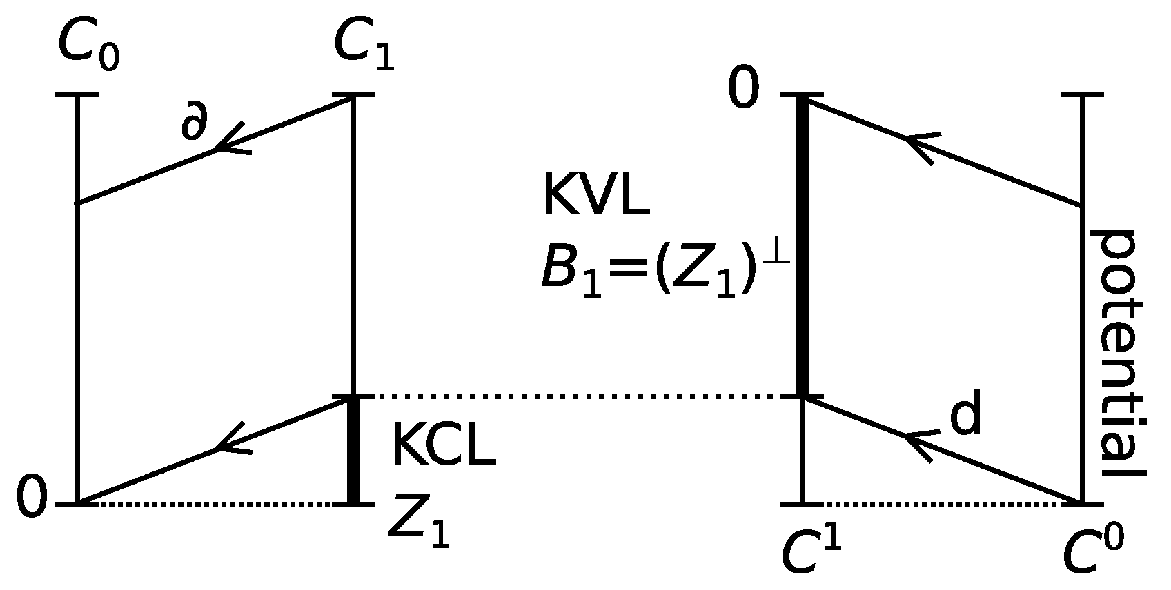
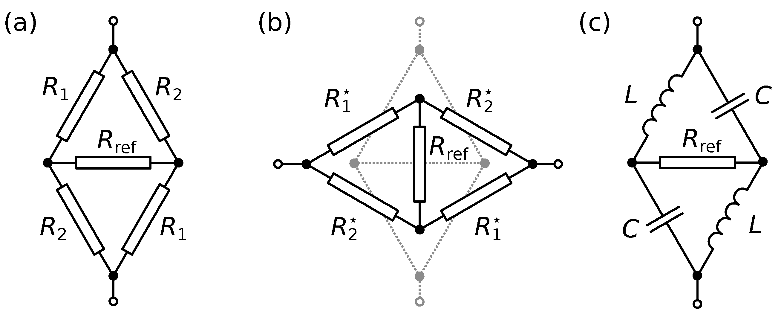
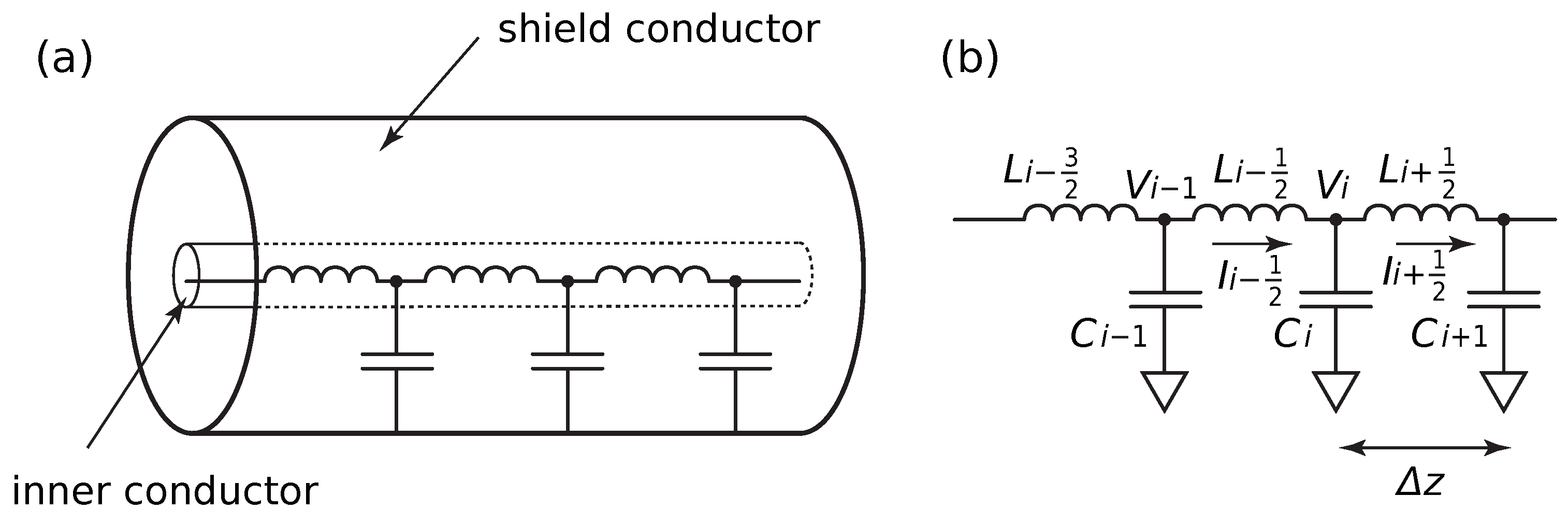
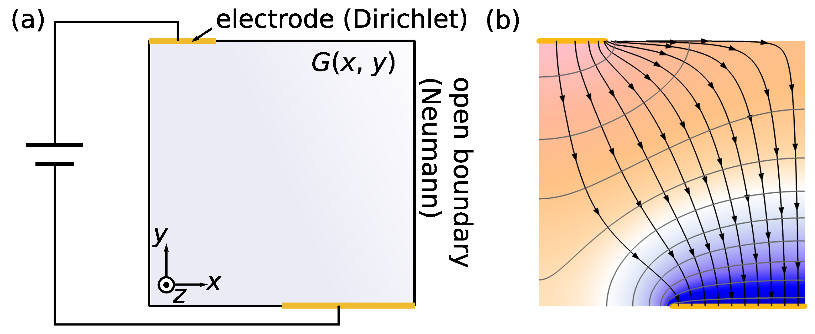
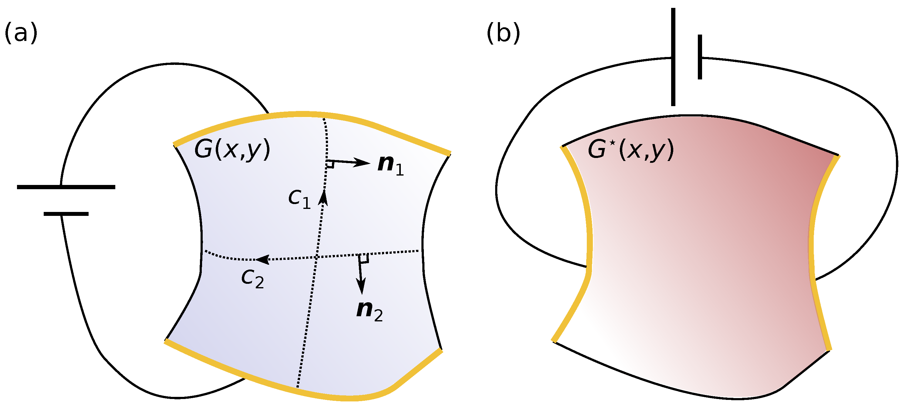
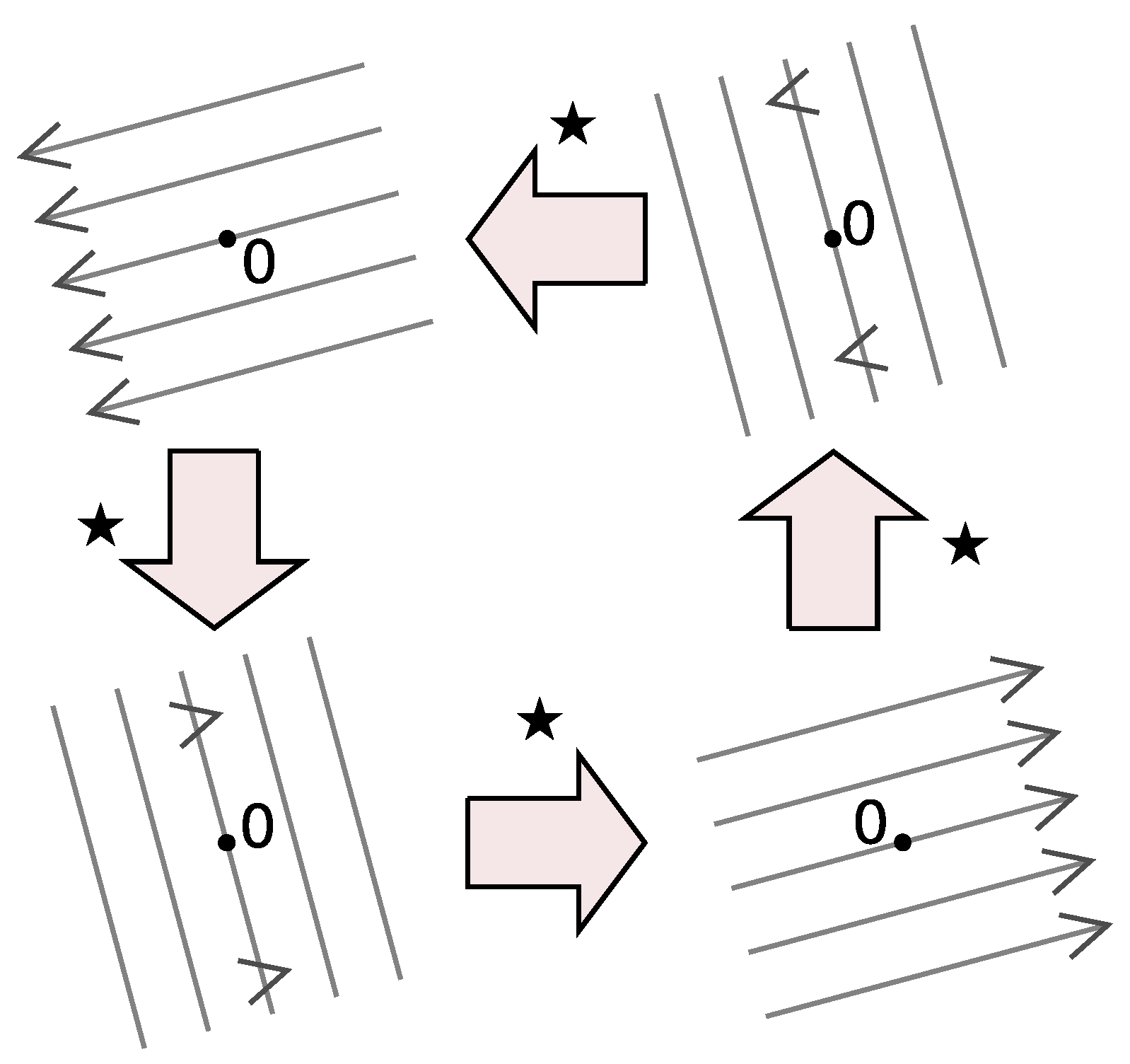
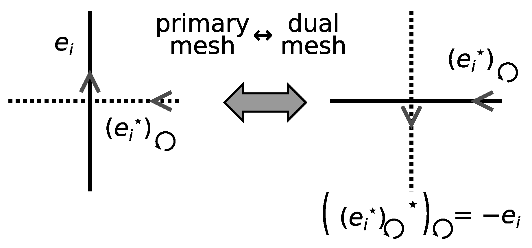
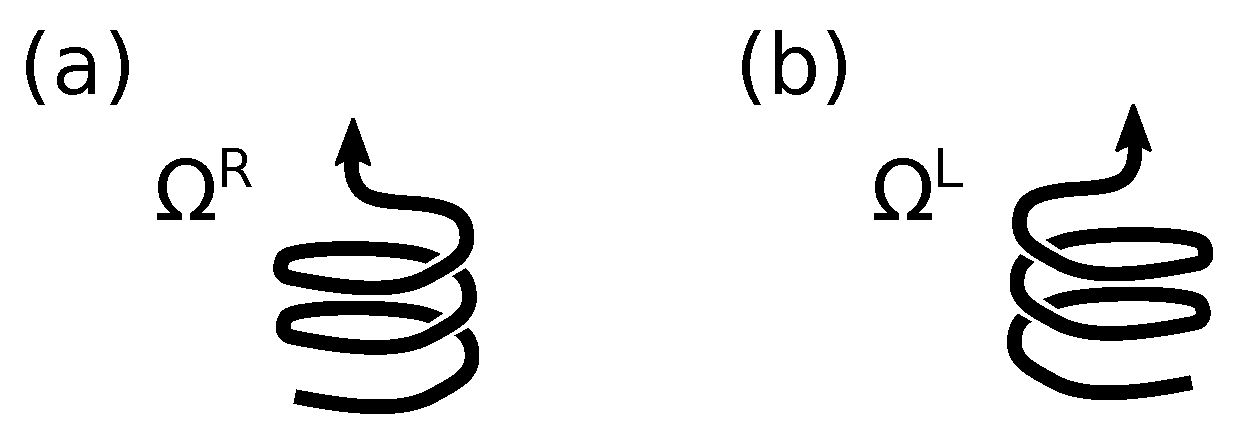
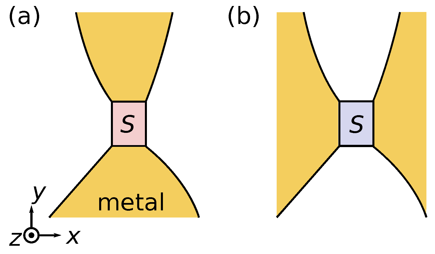
Table 1.
Dual relations in electrical circuits.
| Circuit | Dual Circuit |
|---|---|
| Current distribution I | Voltage distribution |
| Voltage distribution V | Current distribution |
| Face current F | Potential |
| Potential | Face current |
| Voltage source | Current source |
| Current source | Voltage source |
| Resistance R | Conductance |
| Conductance G | Resistance |
© 2019 by the authors. Licensee MDPI, Basel, Switzerland. This article is an open access article distributed under the terms and conditions of the Creative Commons Attribution (CC BY) license (http://creativecommons.org/licenses/by/4.0/).
Share and Cite
MDPI and ACS Style
Nakata, Y.; Urade, Y.; Nakanishi, T. Geometric Structure behind Duality and Manifestation of Self-Duality from Electrical Circuits to Metamaterials. Symmetry 2019, 11, 1336. https://0-doi-org.brum.beds.ac.uk/10.3390/sym11111336
AMA Style
Nakata Y, Urade Y, Nakanishi T. Geometric Structure behind Duality and Manifestation of Self-Duality from Electrical Circuits to Metamaterials. Symmetry. 2019; 11(11):1336. https://0-doi-org.brum.beds.ac.uk/10.3390/sym11111336
Chicago/Turabian StyleNakata, Yosuke, Yoshiro Urade, and Toshihiro Nakanishi. 2019. "Geometric Structure behind Duality and Manifestation of Self-Duality from Electrical Circuits to Metamaterials" Symmetry 11, no. 11: 1336. https://0-doi-org.brum.beds.ac.uk/10.3390/sym11111336
Note that from the first issue of 2016, this journal uses article numbers instead of page numbers. See further details here.