
Electronic Dislocation Dynamics in Metastable Wigner Crystal States
by
 , ,
, ,
Andrej Kranjec
1, 
Petr Karpov
2,3,
Yevhenii Vaskivskyi
1,
Jaka Vodeb
1,
Yaroslav Gerasimenko
1 and
Dragan Mihailovic
1,4,* 1
Jozef Stefan Institute, Jamova 39, SI-1000 Ljubljana, Slovenia
2
Max Planck Institute for Physics of Complex Systems, Nöthnitzer Str. 38, 01187 Dresden, Germany
3
Arnold Sommerfeld Center for Theoretical Physics, Ludwig-Maximilians-Universität München, Theresienstr. 37, 80333 Munich, Germany
4
CENN Nanocenter, Jamova 39, SI-1000 Ljubljana, Slovenia
*
Author to whom correspondence should be addressed.
Symmetry 2022, 14(5), 926; https://0-doi-org.brum.beds.ac.uk/10.3390/sym14050926
Submission received: 30 March 2022
/
Revised: 26 April 2022
/
Accepted: 27 April 2022
/
Published: 1 May 2022
(This article belongs to the Special Issue Topological Objects in Correlated Electronic Systems)
Abstract
:Metastable states appear in many areas of physics as a result of symmetry-breaking phase transitions. An important challenge is to understand the microscopic mechanisms which lead to the formation of the energy barrier separating a metastable state from the ground state. In this paper, we describe an experimental example of the hidden metastable domain state in 1T-TaS2, created by photoexcitation or carrier injection. The system is an example of a charge density wave superlattice in the Wigner crystal limit displaying discommensurations and domain formation when additional charge is injected either through contacts or by photoexcitation. The domain walls and their crossings in particular display interesting, topologically entangled structures, which have a crucial role in the metastability of the system. We model the properties of experimentally observed thermally activated dynamics of topologically protected defects—dislocations—whose annihilation dynamics can be observed experimentally by scanning tunnelling microscopy as emergent phenomena described by a doped Wigner crystal. The different dynamics of trivial and non-trivial topological defects are quite striking. Trivial defects appear to annihilate quite rapidly at low temperatures on the timescale of the experiments, while non-trivial defects annihilate rarely, if at all.
1. Introduction
Metallic transition metal dichalcogenides (TMDs) commonly display commensurate charge-ordering at low temperatures. While some materials have received particularly detailed attention with a focus on specific features, the generic features, and the origin of broken translational symmetry, in particular, cannot be easily described in terms of traditional concepts, such as Fermi surface nesting, exciton condensation phenomena or peculiarities of the electron–phonon interaction occurring in specific systems. On the other hand, a lattice Wigner crystal description appears to offer a common conceptual starting point for discussion not only of the ground-state ordering, but also metastable states in the system. The justification for the lattice Wigner crystal comes from the ratio of the kinetic energy in relation to the Coulomb energy , expressed in terms of the Wigner–Seitz radius , that defines the crossover from Fermi-liquid behaviour to a lattice Wigner crystal state with dominant Coulomb interactions. The ratio of Coulomb energy to kinetic energy defines , where is the electron density, is the elementary charge, and is the effective mass of electron [1]. is strongly dependent on the electron density . In the prototypical dichalcogenide charge-density-wave (CDW) system—1T-TaS2, for example—the electron density is small (one electron per 13 unit cells). Due to strong coupling to the lattice [2], polaronic effects renormalize the electronic bands, which become narrow, resulting in an increase in effective mass [3], which leads to an and carrier localization in the lattice Wigner-crystal limit. There are two consequences: the first is the introduction of Mott physics [4,5], where the ordering dynamics are dominated by the Coulomb interaction, and the second is instability towards domain formation upon external perturbation or doping that takes place in the form of a symmetry-breaking transition.
The domains in such electronic crystals display very rich physics [6,7,8,9]. For example, the structure of domains created by laser excitation displays intertwined orders and intricate chiral ordering [9]. The structure of domain walls (DWs) themselves has been addressed on different levels [10,11,12,13]. In the context of Wigner crystal domains, Karpov and Brazovskii [10] introduced fractional charges associated with different mutual domain configurations. On a microscopic level, domain walls were analysed with scanning tunnelling microscopy in combination with density-functional-theory calculations [10,11,12,13], revealing the electronic structure within DWs. However, such modelling cannot be used to understand domain formation kinetics, the origins of metastability [14], or the dynamics of domain relaxation, governed by spatial topological constraints; nor can it be used to predict the generic formation of commensurate and domain structures across the entire series of metallic TMDs. The first step toward understanding such phenomena is the experimental characterization of the topology of the domain structure.
Here, we present an experimental analysis of the domain wall junctions, analysing the vertex structure in terms of 2D classical edge dislocations. Real-time measurements of domain relaxation using scanning tunnelling microscopy show the possibility of measuring dislocation annihilation dynamics.
2. Experimental Results
At low temperature (<140 K), the unperturbed ground state in 1T-TaS2 is an electronic superlattice with a filling of 1/13 with respect to the atomic triangular lattice, which is commonly referred to as the commensurate charge-density-wave (CCDW or C-state). The superlattice vector is given by , where and are the fundamental crystal lattice vectors (Figure 1a), the stars signify the polaronic distortions around extra electron charge on the Ta atom at the centre of each star-of-David hexagram. Domains are ubiquitously observed when a charge is injected by a large STM tip current pulse [6], an electrical pulse through contacts of a device [8], or by photoexcitation (photodoping), where the effect was originally discovered [14]. The resulting ‘hidden’ (H) domain state is metastable and has a lifetime that is sufficiently long that its domain structure can be investigated in detail at low temperatures [15].
In the present work, we excite in situ cleaved single crystals of 1T-TaS2 at 4.2 K with a voltage pulse from the tungsten tip of an STM. The area around the location of the voltage pulse is first probed to determine where the hidden state borders the surrounding CCDW. When an appropriate area is found, we let the STM scanning run until at least several frames are acquired and a substantial relaxation is observed. Typical domain-forming pulse parameters are V = 4 V, pulse duration 1 ms and tunnel junction resistance 1 GΩ.
To study the topological properties of the domain network, we need to accurately determine domains’ phase shifts, fitting them on the underlying atomic lattice. To this end, we employ a simulated annealing Monte Carlo (MC) algorithm: first, we determine the most probable values of phase shifts for each neighbouring pair of domains, which we then globally optimize for the whole domain network. Such a local procedure supplemented by global “sewing” helps us to determine the domains’ phases, even for big STM images which exhibit non-uniform values of the underlying lattice constant or lattice rotation angle.
Using the above procedure, we analyse a large area domain structure formed by STM tip current injection shown in Figure 1b. The domain walls cross, typically forming three or four-pronged vertices. The vertices may be trivial, or non-trivial, according to whether a Burger’s vector construction around the vertex is zero (), or non-zero (), to which we refer as trivial () and non-trivial () vertices, respectively. In Figure 1b, vertices are labelled according to whether the Burger’s vector construction is (no arrow), or (the yellow arrow shows ). Figure 1c,d show examples of and a vertices, respectively. The corresponding Burgers circuit construction in each case is shown in Figure 1e,f. The construction is always made, along with the shortest possible interdomain shifts upon crossing a domain wall, which is either of the nearest-neighbour types, with length , or the next nearest-neighbour type with length (Figure 1e,f). We emphasize that the Burgers vector construction does not depend on the detailed structure of the vertex or the presence of extrinsic defects in its vicinity.
A relaxation sequence of the H state induced by a voltage pulse from the STM tip is shown in Figure 2. The domain area is entirely surrounded by the C-state (red overlay). The panels a–b6 show a gradual diminishing of the H-state and expansion of the C-state in discrete steps. Each frame was analysed by the MC-simulated annealing algorithm to determine the presence of dislocations at vertices. The vertices are labelled according to how many domains are adjacent to the vertex, which is the first number, and whether they are trivial () or non-trivial (). The arrows next to non-trivial vertices indicate their Burgers vector, yellow for and white for . Panels b1–b6, with overlaid Burgers vectors, display the dislocation dynamics. We observe a constant number of dislocations in the domain reconfiguration process until the last frame, where two dislocations with opposite Burgers vectors annihilate. The latter two are marked by blue circles on image b5 prior to annihilation. Movement of some dislocations is also observed (which we attribute to a combination of climb and glide—see Figure 3).
The panels c1–c6 show the same time evolution with colour maps for domains generated by the MC algorithm. The colouring of domains is according to their shift with respect to the original reference domain (which is chosen to be the C-state) following the colouring scheme of Figure 1a. We note that the colouring of domains remains consistent throughout the relaxation in the sense that domains do not change the CDW phase until they disappear. This is to be expected, since it is energetically costly to change the phase shift of a whole domain. They do, however, change their shape and size during relaxation.
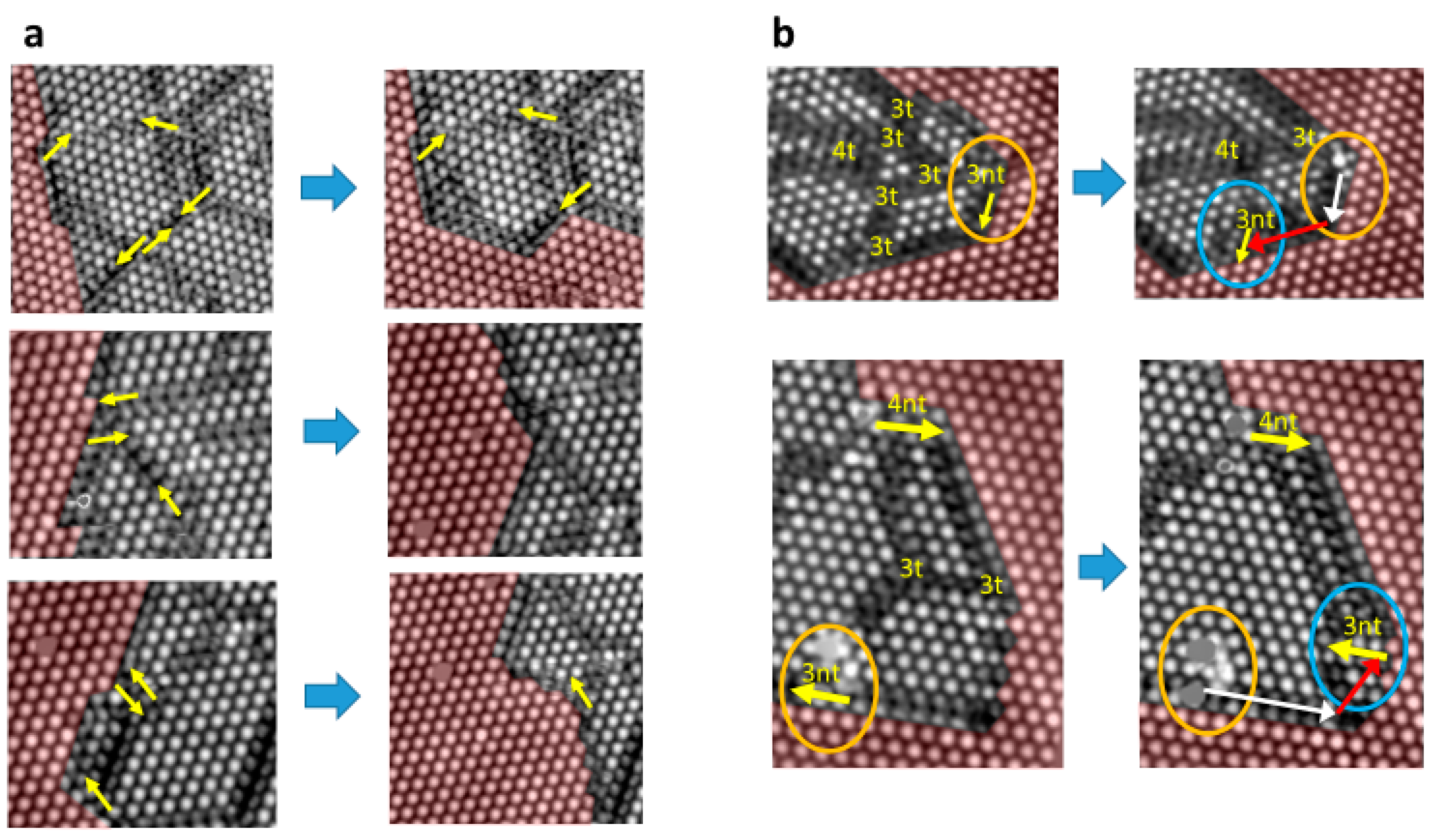
Annihilation, glide and climb. Figure 3a shows three examples of dislocation pair annihilation in subsequent frames. In the middle panel, three dislocations disappear; in the last panel, two dislocations annihilate, and one is displaced. Yellow arrows are Burgers vectors, red shading indicates the surrounding CCDW. Figure 3b shows two examples of dislocation ( vertex) displacements, which we can attribute to a combination of glide and climb motion, as indicated by the different-coloured arrows (glide: white, climb: red). Glide motion involves motion along the direction of , while climb involves motion at an angle of either or to .
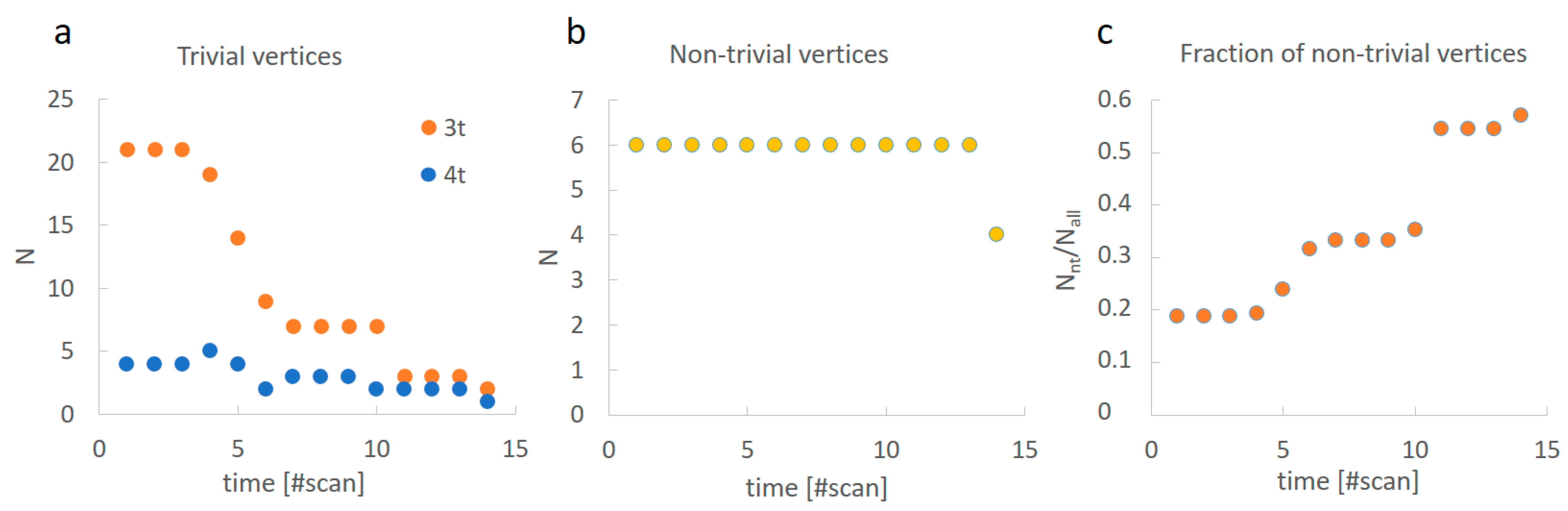
Annihilation dynamics. By examining STM frames in sequence, we can obtain an idea of the different rates of dislocation annihilation. While the amount of data is limited by the small number of frames and the slow relaxation rate, we can clearly distinguish different relaxation rates for different types of vertices. Figure 4 shows a count of the number of and vertices for three- and four-pronged vertices on the full STM sequence of images shown in Figure 2. The three-pronged vertices appear to show relaxation on the timescale of tens of minutes. In contrast, the four-pronged vertices show much slower dynamics. This is possibly due to the fact that most vertices are located closer to the border with the CCDW, or simply due to the fact that they have more phase constraints and are therefore more energetically costly to relax. The defects show very little dynamics on this timescale. The number of dislocations is constant until the last frame (when two dislocations annihilate) and so they form a sort of stable backbone of the domain wall network. It is clear from the examination of the STM images that and vertices are inextricably entangled with each other in the sense that vertex and anti-vertex pairs are not adjacent to each other, but there may be other vertices geometrically constraining their annihilation. It is quite likely that some defects have their anti-defects outside the image area, and the present experiments are limited in this way. Nevertheless, the general trend is clear. We also note that the fraction of vertices increases during relaxation, making the hidden state more topologically protected. This could have implications for data retention in memory-device applications.
3. Domain Textures as an Emergent Phenomenon
To understand the formation of domains, one may approach it from different directions [9,10,11,12,13,14,16,17]. A generally applicable theory with useful predictive value considers the domain structure as an emergent property, as a response of the polaronic Wigner crystal to doping [10,14,16]. The model Hamiltonian is given by [16]:
where or is the occupation number of a polaron on the site 𝑖, and
is the Yukawa screening potential, where in CGS units and , where is the dimensionless position of the i-th polaron, and is the dimensionless screening radius. is the dielectric constant of the material. The use of the model for quasi-2D transition metal dichalcogenides has been justified previously, and has predicted the existence of electronic superlattices at magic-filling fractions and domains or amorphous electronic structures in between. Details of the calculation can be found in Ref. [16].
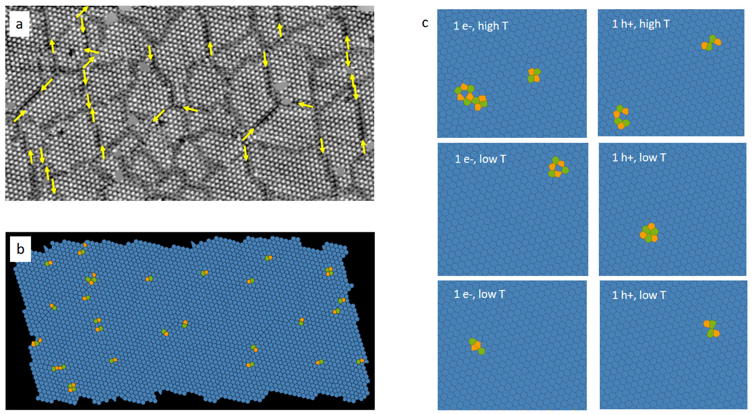
One possible way to represent the topological defects in the data is by using Wigner–Seitz cell (or sometimes called Voronoi) constructions around each polaron. Figure 5b shows such a construction for the large area experimental STM image with a large density of dislocations in Figure 5a. As before, the domains are first put to the underlying lattice with the MC simulated annealing process. Hexagons are coloured blue, while pentagons and heptagons are coloured orange and green, respectively. We see that vertices indicated by the arrows (which have non-zero ) are associated with heptagon–pentagon pairs. These are topologically equivalent to dislocations on a hexagonal lattice. The Wigner–Seitz cell representation is thus a useful abstraction for the rather complicated domain structure observed in STM experiments.
The results of the calculation for lightly doped (adding 1 electron or 1 hole) Wigner crystal with a magic filling fraction of 1/13 are shown in Figure 5c in the form of a Wigner–Seitz cell plot. We see that doping creates topological defects in the form of pentagon–heptagon pairs, irrespective of the temperature. At higher temperatures, additional defects are visible due to pair excitations appearing as fluctuations in the number density. Comparing the predictions of this classical polaronic lattice gas model (Figure 5c) with the experiment in Figure 5b, we see that the model predicts the formation of the same kind of defects associated with doping. In both cases, we can see paired dislocations. The difference is in the presence of single heptagon–pentagon pairs in the experimental image, while in the model they are all paired or clustered. The comparison strongly suggests that the vertices are associated with an extra trapped charge.
Our simulations also show that the number of defects increases as we increase doping in the system and when doping is zero, no defects are remaining. Therefore, from the point of view of our polaronic Wigner crystal approach, the domain formation mechanism is the following. Photoexcitation or charge injection introduces additional charges in the system. Karpov and Brazovskii [10] have already shown that a domain wall is energetically more favourable than a hole or interstitial charge; therefore, a network of domain walls forms. The number of topologically protected defects is governed by the doping level and this number does not change if the doping level remains the same. Trivial defects, however, can relax and disappear. Experimentally, it was noted before [16] that the doping level differs in the ground state and metastable state, which suggests that extra charges responsible for topologically protected defects also eventually leak back into the Fermi sea below the Fermi level.
4. Discussion
‘Standard’ theory of domain walls in CDW systems considers the energy of DW formation and energy of DW crossings (DWCs), which are of opposite signs, such that the two form a metastable minimum in the free energy of the system [14,18,19,20,21]. The minimum corresponds to a particular, topologically protected domain state, in the sense that the minimum is determined by specific details of the material and is immune to external single-particle perturbations. However, this does not include the additional complication of real-space pinning defects, nor is it immune to strain, for example [15]. In the same sense, the domain size is controlled by carrier injection [14,22,23]. The self-organized intrinsic formation of topological defects at DW crossings observed above is not included in the theory, yet it is likely to have a significant effect on the system stability, and hence the free-energy potential landscape. The dynamics of dislocations in particular are governed by annihilation dynamics, the bottleneck being matched defect pair annihilation. In 2D, conventional Kosterlitz–Thouless (K-T) theory, the dynamics are discussed in terms of edge dislocations, which are created and annihilated in pairs. At high density, the dislocations destroy long-range order, resulting in a hexatic phase. When the dislocations dissociate into five- and seven-fold disclinations, an additional isotropic phase may appear. The two-step melting of such a phase is described in terms of the Kosterlitz–Thouless–Halperin–Nelson–Young (KTHNY) theory with two consecutive K-T transitions. These theories do not consider the dynamics of the dislocations, which can be quite intricate.
The dynamics of classical lattice dislocations under stress is governed by a Peach–Koehler (P-K) force between dislocations described in terms of their Burger’s vector and the stress tensor, with additional terms arising from pinning by extrinsic defects, temperature-driven lattice fluctuations, local (Peierls-Nabarro) strains, etc. [24,25]. Simulations of the dynamics in classical 2D systems typically reveal aggregation of dislocations in the form of clusters, and at the edges.
In the case of an electronic crystal on a hexagonal lattice, the structure of non-trivial defects is formally equivalent to lattice dislocations, but the microscopic structural details, on which the dynamics will depend, are quite specific. The experimental data above show the structure of trivial and non-trivial vertex dynamics and are presented formally in terms of dislocation dynamics. Aggregation of dislocations at the edges or in the centre of the domain structures is not observed on the timescale of the STM experiments, suggesting that annihilation is faster than the P-K dynamics at 4 K. More importantly, the dynamics is governed by the entanglement of defect pairs, which prevents direct annihilation of defect–anti-defect pairs through a simple glide or climb motion, but requires ‘circumnavigation’ and annihilation in a particular sequence. The fact that the domains are created spontaneously, from initial fluctuation–nucleation after a quench suggests some degree of randomness in the initial distribution of defects. However, domain-wall repulsion and the energy gained by crossings at vertices act to form a more uniform, long-ranged order in the domain structure. The latter process is hindered by topological constraints at the vertices.
We note that the present analysis is limited to the temporal and spatial window of the STM experiments. Dynamics on other timescales cannot be excluded, but currently, there are no other methods to observe the defect dynamics. In spite of experimental limitations, the dynamics of the observed difference in and dynamics are quite significant, indicating that the forces between and are quite different. An additional complication arises from the fact that and vertices are intertwined, which brings a complex topology to the problem.
On a phenomenological level, the relaxation was previously described in terms of the Ostwald ripening process, with double exponential relaxation, but the approach is not very insightful in explaining the magnitude of the energy barrier for relaxation to the ground state [15]. However, the strong observed sensitivity of to external strain suggests that a general P-K approach is reasonable.
A suitable framework for describing the quantum nature of such a system may be provided by fractions, excitations within a tensorial field theory that are dual to classical elasticity theory used in the present analysis [26], but such treatment is beyond the scope of this paper.
Given that the detailed construction of DWCs is likely to play an important role in the overall relaxation process of the electronic Wigner crystal, one may comment on the prospect of dealing with the dynamics of such a system on the microscopic level (e.g., density functional theory) used recently to describe the static structure of single DWs. Such modelling may be useful in determining the relative energy stability of different DWs and eventually DWCs. The transitions between states on the resulting energy landscape may form the basis of more material-specific relaxation dynamics.
5. Conclusions
The difference in and dynamics is striking and proves that the topological protection of vertices plays a crucial role in the stability of the domain state. We conclude by commenting on the fact that at low temperatures, the dynamics are limited by macroscopic quantum tunnelling between different, but energetically near-degenerate domain configurations that were shown, in recent experiments, to be finite [27].
Author Contributions
Conceptualization, D.M., A.K., Y.G. and Y.V.; methodology, P.K., A.K. and D.M.; software, P.K., A.K. and J.V.; formal analysis, A.K., P.K. and J.V.; writing—original draft preparation, D.M. and A.K.; writing—review and editing, D.M., A.K., P.K., Y.V. and J.V.; funding acquisition, D.M. All authors have read and agreed to the published version of the manuscript.
Funding
This research was funded by the Slovenian Research Agency, grant P1-0040 and A.K. to PR-06158. We thank the CENN Nanocenter for the use of its facilities.
Data Availability Statement
Not applicable.
Acknowledgments
We thank the CENN Nanocenter for the use of its facilities, Petra Šutar for the samples used in this work, and Maksim Litskevich for the help with measurements.
Conflicts of Interest
The authors declare no conflict of interest.
References
- Schrieffer, J.R. Theory of Superconductivity; Westview Books: Boulder, CO, USA, 1964; ISBN 0738201200. [Google Scholar]
- Machida, Y.; Hanashima, T.; Ohkubo, K.; Yamawaki, K.; Tanaka, M.; Sasaki, S. Observation of Soft Phonon Modes in 1T-TaS 2by Means of X-ray Thermal Diffuse Scattering. J. Phys. Soc. Jpn. 2004, 73, 3064–3069. [Google Scholar] [CrossRef]
- Rossnagel, K. On the Origin of Charge-Density Waves in Select Layered Transition-Metal Dichalcogenides. J. Phys. Condens. Matter 2011, 23, 213001. [Google Scholar] [CrossRef] [PubMed]
- Fazekas, P.; Tosatti, E. Charge Carrier Localization in Pure and Doped 1T-Tas2. Phys. B+C 1980, 99, 183–187. [Google Scholar] [CrossRef]
- Tosatti, E.; Fazekas, P. On the Nature of the Low-Temperature Phase of 1T-TaS2. J. Phys. Colloq. 1976, 37, C4-165–C4-168. [Google Scholar] [CrossRef] [Green Version]
- Ma, L.; Ye, C.; Yu, Y.; Lu, X.F.; Niu, X.; Kim, S.; Feng, D.; Tománek, D.; Son, Y.W.; Chen, X.H.; et al. A Metallic Mosaic Phase and the Origin of Mott-Insulating State in 1T-TaS2. Nat. Commun. 2016, 7, 10956. [Google Scholar] [CrossRef]
- Cho, D.; Cheon, S.; Kim, K.-S.; Lee, S.-H.; Cho, Y.-H.; Cheong, S.-W.; Yeom, H.W. Nanoscale Manipulation of the Mott Insulating State Coupled to Charge Order in 1T-TaS2. Nat. Commun. 2016, 7, 10453. [Google Scholar] [CrossRef] [Green Version]
- Vaskivskyi, I.; Mihailovic, I.A.; Brazovskii, S.; Gospodaric, J.; Mertelj, T.; Svetin, D.; Sutar, P.; Mihailovic, D. Fast Electronic Resistance Switching Involving Hidden Charge Density Wave States. Nat. Commun. 2016, 7, 11442. [Google Scholar] [CrossRef]
- Gerasimenko, Y.A.; Karpov, P.; Vaskivskyi, I.; Brazovskii, S.; Mihailovic, D. Intertwined Chiral Charge Orders and Topological Stabilization of the Light-Induced State of a Prototypical Transition Metal Dichalcogenide. npj Quantum Mater. 2019, 4, 32. [Google Scholar] [CrossRef]
- Karpov, P.; Brazovskii, S. Modeling of Networks and Globules of Charged Domain Walls Observed in Pump and Pulse Induced States. Sci. Rep. 2018, 8, 4043. [Google Scholar] [CrossRef] [Green Version]
- Cho, D.; Gye, G.; Lee, J.; Lee, S.-H.; Wang, L.; Cheong, S.-W.; Yeom, H.W. Correlated Electronic States at Domain Walls of a Mott-Charge-Density-Wave Insulator 1 T-TaS 2. Nat. Commun. 2017, 8, 392. [Google Scholar] [CrossRef]
- Park, J.W.; Cho, G.Y.; Lee, J.; Yeom, H.W. Emergent Honeycomb Network of Topological Excitations in Correlated Charge Density Wave. Nat. Commun. 2019, 10, 4038. [Google Scholar] [CrossRef] [PubMed] [Green Version]
- Park, J.W.; Lee, J.; Yeom, H.W. Zoology of Domain Walls in Quasi-2D Correlated Charge Density Wave of 1T-TaS2. NPJ Quantum Mater. 2021, 6, 32. [Google Scholar] [CrossRef]
- Stojchevska, L.; Vaskivskyi, I.; Mertelj, T.; Kusar, P.; Svetin, D.; Brazovskii, S.; Mihailovic, D. Ultrafast Switching to a Stable Hidden Quantum State in an Electronic Crystal. Science 2014, 344, 177–180. [Google Scholar] [CrossRef] [PubMed] [Green Version]
- Vaskivskyi, I.; Gospodaric, J.; Brazovskii, S.; Svetin, D.; Sutar, P.; Goreshnik, E.; Mihailovic, I.A.; Mertelj, T.; Mihailović, D. Controlling the Metal-to-Insulator Relaxation of the Metastable Hidden Quantum State in 1T-TaS2. Sci. Adv. 2015, 1, e1500168. [Google Scholar] [CrossRef] [Green Version]
- Vodeb, J.; Kabanov, V.V.; Gerasimenko, Y.A.; Venturini, R.; Ravnik, J.; van Midden, M.A.; Zupanic, E.; Sutar, P.; Mihailovic, D. Configurational Electronic States in Layered Transition Metal Dichalcogenides. New J. Phys. 2019, 21, 083001. [Google Scholar] [CrossRef]
- Ravnik, J.; Diego, M.; Gerasimenko, Y.; Vaskivskyi, Y.; Vaskivskyi, I.; Mertelj, T.; Vodeb, J.; Mihailovic, D. A Time-Domain Phase Diagram of Metastable States in a Charge Ordered Quantum Material. Nat. Commun. 2021, 12, 2323. [Google Scholar] [CrossRef]
- Villain, J. Commensurate-Incommensurate Transition of Krypton Monolayers on Graphite: A Low Temperature Theory. Surf. Sci. 1980, 97, 219–242. [Google Scholar] [CrossRef]
- Bak, P.; Mukamel, D.; Villain, J.; Wentowska, K. Commensurate-Incommensurate Transitions in Rare-Gas Monolayers Adsorbed on Graphite and in Layered Charge-Density-Wave Systems. Phys. Rev. B 1979, 19, 1610. [Google Scholar] [CrossRef]
- Bak, P. Commensurate Phases, Incommensurate Phases and the Devil’s Staircase. Rep. Prog. Phys. 1982, 45, 587–629. [Google Scholar] [CrossRef]
- Brazovskii, S. Modeling of Evolution of a Complex Electronic System to an Ordered Hidden State: Application to Optical Quench in 1T-TaS2. J. Supercond Nov. Magn. 2015, 28, 1349–1353. [Google Scholar] [CrossRef]
- Brazovskii, S. Coherent Topological Defect Dynamics and Collective Modes in Superconductors and Electronic Crystals. Available online: http://0-iopscience-iop-org.brum.beds.ac.uk/0953-8984/25/40/404206/pdf/0953-8984_25_40_404206.pdf (accessed on 12 March 2022).
- Brazovskii, S.; Kirova, N.; Requardt, H.; Nad, F.Y.; Monceau, P.; Currat, R.; Lorenzo, J.E.; Grübel, G.; Vettier, C. Plastic Sliding of Charge Density Waves: X-ray Space Resolved-Studies versus Theory of Current Conversion. Phys. Rev. B 2000, 61, 10640. [Google Scholar] [CrossRef]
- Roters, F.; Eisenlohr, P.; Hantcherli, L.; Tjahjanto, D.D.; Bieler, T.R.; Raabe, D. Overview of Constitutive Laws, Kinematics, Homogenization and Multiscale Methods in Crystal Plasticity Finite-Element Modeling: Theory, Experiments, Applications. Acta Mater. 2010, 58, 1152–1211. [Google Scholar] [CrossRef]
- Lubarda, V.A. Dislocation Burgers Vector and the Peach–Koehler Force: A Review. J. Mater. Res. Technol. 2019, 8, 1550–1565. [Google Scholar] [CrossRef]
- Pretko, M.; Radzihovsky, L. Fracton-Elasticity Duality. Phys. Rev. Lett. 2018, 120, 195301. [Google Scholar] [CrossRef] [Green Version]
- Vodeb, J.; Diego, M.; Vaskivskyi, Y.; Gerasimenko, Y.; Kabanov, V.; Mihailovic, D. Observation of Quantum Domain Melting and Its Simulation with a Quantum Computer. arXiv 2021, arXiv:2103.07343. [Google Scholar]
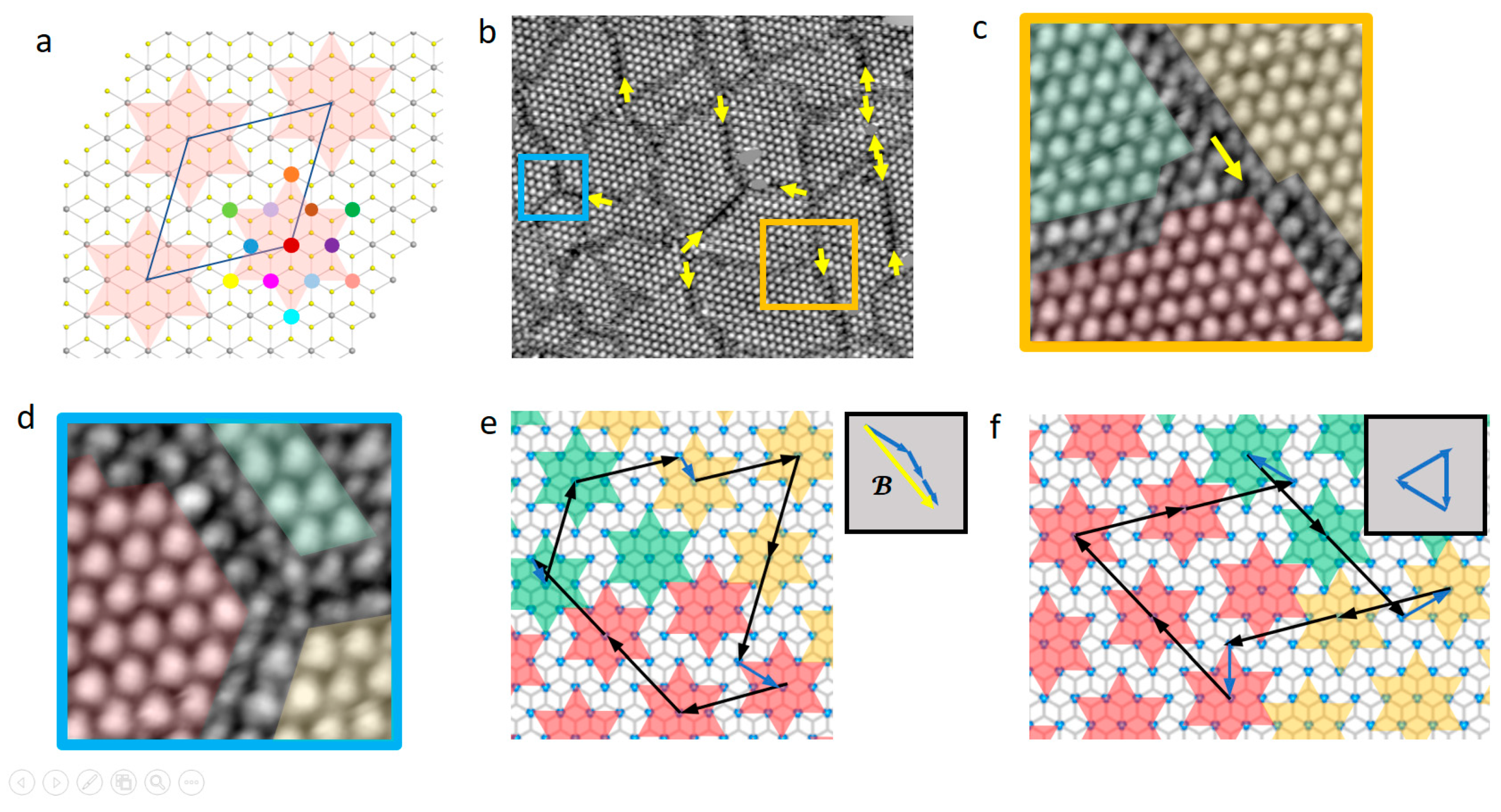
Figure 1.
(a) Schematic representation of the commensurate superlattice showing twelve possible interdomain phase shifts with the corresponding colour coding. The parallelogram shows the CDW superlattice unit cell. (b) STM image (V = −800 mV) of a part of the domain state with a relatively high density of dislocations. Yellow arrows indicate non-zero Burgers vectors at the vertices. (c) Zoom-in of the orange square on (b), rotated to align the underlying atomic lattice with the horizontal axis. Colour shading indicates different domains. A yellow arrow represents the Burgers vector. (d) Same as in (c) for a trivial vertex marked with the blue square in (b). (e) A schematic representation of the 3-vertex in (c). Blue circles are tantalum atoms; star of David overlays represent polarons using the same colour scheme as (c). Black arrows are CDW superlattice vectors indicating the Burgers circuit around the vertex. Blue vectors are relative shifts of domains upon crossing a domain wall. The inset shows that the relative shifts add up to a CDW superlattice vector, the Burgers vector of the vertex. (f) Same as in (e) for the trivial vertex. The inset of image 9 (f) shows that relative shift vectors add up to zero. Note that all domain wall types are the most common ones observed as reported previously in Ref. [13].

Figure 2.
Relaxation sequence of the hidden state induced by a voltage pulse from the STM tip. (a,b) Analysed STM sequence of the relaxation of a patch of hidden state surrounded by the CCDW. Vertices are marked by yellow markings, with the number representing the number of domains that meet at a vertex and the letters “t” and “nt” stand for trivial and non-trivial, respectively (3nt = non-trivial 3-vertex). The yellow arrow next to non-trivial vertices indicate their Burgers vector. Red shading indicates the surrounding CCDW and the domain, which is not shifted with respect to the CCDW. Blue circles in frames 4- and 5-mark pairs of dislocations that annihilate in the next frame. (c) Colour maps of domains for each frame in (a,b) as a result of the Monte Carlo algorithm. Colours correspond to relative domain shifts according to Figure 1d, with the origin (red) chosen as the CCDW. The colour of lines connecting centres of domains represents the quality of recognition of the MC algorithm. Green edges correspond to the best reliability, orange to lesser, red even less and black poor recognition. The vast majority of lines in all frames are green indicating reliable interdomain shift recognition. White lines in the CCDW are used to cut it into smaller pieces for better algorithm recognition.

Figure 3.
(a) Relaxation events involving annihilation of non-trivial defects. The Burger’s vectors are indicated by the yellow arrows; (b) two examples of glide and climb motion of dislocations. The red overlay represents the bordering CCDW.
Figure 3.
(a) Relaxation events involving annihilation of non-trivial defects. The Burger’s vectors are indicated by the yellow arrows; (b) two examples of glide and climb motion of dislocations. The red overlay represents the bordering CCDW.

Figure 4.
Temporal dynamics of (a) trivial () and (b) non-trivial () vertex relaxation, respectively in consecutive STM scans. Each scan takes around 20 min. (Note the different scales.) (c) The number of vertices as a fraction of the total number of vertices.
Figure 4.
Temporal dynamics of (a) trivial () and (b) non-trivial () vertex relaxation, respectively in consecutive STM scans. Each scan takes around 20 min. (Note the different scales.) (c) The number of vertices as a fraction of the total number of vertices.

Figure 5.
Comparison of an experimental image with the MC lattice gas model. (a) An STM image with a relatively high density of dislocations. Yellow arrows are Burgers vectors. (b) Wigner–Seitz cell diagram of the MC lattice fit to the image in (a). (c) Wigner–Seitz cells of the MC lattice gas model simulation after adding an electron (e-), or a hole (h+) to the lattice at different effective temperatures. Colour code: hexagons (blue), pentagons (orange), and heptagons (green).

Publisher’s Note: MDPI stays neutral with regard to jurisdictional claims in published maps and institutional affiliations. |
© 2022 by the authors. Licensee MDPI, Basel, Switzerland. This article is an open access article distributed under the terms and conditions of the Creative Commons Attribution (CC BY) license (https://creativecommons.org/licenses/by/4.0/).
Share and Cite
MDPI and ACS Style
Kranjec, A.; Karpov, P.; Vaskivskyi, Y.; Vodeb, J.; Gerasimenko, Y.; Mihailovic, D. Electronic Dislocation Dynamics in Metastable Wigner Crystal States. Symmetry 2022, 14, 926. https://0-doi-org.brum.beds.ac.uk/10.3390/sym14050926
AMA Style
Kranjec A, Karpov P, Vaskivskyi Y, Vodeb J, Gerasimenko Y, Mihailovic D. Electronic Dislocation Dynamics in Metastable Wigner Crystal States. Symmetry. 2022; 14(5):926. https://0-doi-org.brum.beds.ac.uk/10.3390/sym14050926
Chicago/Turabian StyleKranjec, Andrej, Petr Karpov, Yevhenii Vaskivskyi, Jaka Vodeb, Yaroslav Gerasimenko, and Dragan Mihailovic. 2022. "Electronic Dislocation Dynamics in Metastable Wigner Crystal States" Symmetry 14, no. 5: 926. https://0-doi-org.brum.beds.ac.uk/10.3390/sym14050926
Note that from the first issue of 2016, this journal uses article numbers instead of page numbers. See further details here.