
Irregular Resistive Switching Behaviors of Al2O3-Based Resistor with Cu Electrode

Division of Electronics and Electrical Engineering, Dongguk University, Seoul 04620, Korea
*
Author to whom correspondence should be addressed.
Metals 2021, 11(4), 653; https://0-doi-org.brum.beds.ac.uk/10.3390/met11040653
Submission received: 24 March 2021
/
Revised: 9 April 2021
/
Accepted: 13 April 2021
/
Published: 17 April 2021
(This article belongs to the Special Issue Machine Learning Methods and Sustainable Development: Metal Oxides and Multilayer Metal-Oxides)
Abstract
:In this work, we examined the irregular resistive switching behaviors of a complementary metal–oxide–semiconductor (CMOS)-compatible Cu/Al2O3/Si resistor device. X-ray photoelectron spectroscopy (XPS) analysis confirmed the chemical and material compositions of a Al2O3 thin film layer and Si substrate. Bipolar resistive switching occurred in a more stable manner than the unipolar resistive switching in the device did. Five cells were verified over 50 endurance cycles in terms of bipolar resistive switching, and a good retention was confirmed for 10,000 s in the high-resistance state (HRS) and the low-resistance state (LRS). Both high reset current (~10 mA) and low reset current (<100 μA) coexisted in the bipolar resistive switching. We investigated nonideal resistive switching behaviors such as negative-set and current overshoot, which could lead to resistive switching failure.
1. Introduction
Since significant memory characteristics were first reported in metal oxides such as NiO and TiO2 in 2005, resistive random-access memory (RRAM) memory has been extensively studied [1,2,3,4]. Early studies were conducted with a focus on unipolar resistive switching (URS) [1,2,3,4]. Among many metal oxides, NiO has been shown to have the most stable URS properties [1]. URS has the advantage that a diode can be used as a selection element in a cross-point structure because switching occurs at one polarity [5]. For a unipolar-type memory device, the first method that was introduced involved forming a diode through a high-temperature process, and then depositing a memory device on it. However, in the case of this structure, the scalability of stacking into two layers and four layers is insufficient due to the high-temperature process of the selection device. Moreover, URS has a disadvantage in that the reset current is too high for joule heating, or that the variation in switching parameters, such as the set and reset voltage, and high-resistance state (HRS) and low-resistance state (LRS) in the cycle-to-cycle and cell-to-cell, is large [1]. On the other hand, the phenomenon of bipolar resistive switching (BRS) in metal oxides has also been reported [6,7,8,9,10,11,12,13,14,15,16,17]. The set and reset processes occur at opposite polarities. The reset process is mainly induced by the electric field. The valence change model and the conductive bridge model are the most common bipolar switching types, and these are determined by the metal top electrode. Cu and Ag can diffuse through the insulating layer, and the conducting filament is formed by the cation ion [18,19,20,21]. On the other hand, the oxygen vacancies are modulated in the oxide and the conductance can be changed by the applied voltage [22]. It should be noted that HfO2, Al2O3, and Ta2O5 achieved much more stable resistive switching behaviors [23,24,25,26] and higher endurances than the URS did. Ovonic threshold switching (OTS) [27] has recently become the most competitive selector element that provides bidirectional nonlinear function for RRAM. Therefore, BRS is now a more dominant research area in the RRAM community than URS is.
Conductive bridge memory has the advantages of a fast switching speed and low-current operation, but unstable resistive switching can occur due to the current overshoot and negative-set behavior [28].
RRAM goes beyond simple nonvolatile memory storage devices, and it can be extended to many applications such as logic devices [29] and neuromorphic devices [30,31,32,33,34,35].
In this work, a Cu/Al2O3/Si device was fabricated and its resistive switching behaviors were investigated. The Al2O3/Si stack was verified by XPS analysis; the analysis confirmed similar I–V characteristics with bipolar resistive switching from several cells. The basic memory device properties, such as cycle-to-cycle variation, endurance, and retention, were tested. Moreover, nonideal resistive switching behaviors like the current overshoot and negative-set behavior were studied as well. Finally, we demonstrated the resistive switching by pulses in nonideal cases.
2. Materials and Methods
The Cu/Al2O3/Si memory device was fabricated using the following process: First, a highly doped Si substrate as the bottom electrode was formed by ion-implantation, wherein the dose was 5 × 10¹⁵ and the energy was 40 keV. Next, a 3.5 nm-thick Al2O3 resistive switching layer was deposited using an atomic layer deposition (ALD) system using precursors of Al(CH3)3 (TMA) and O3 at a chamber temperature of 350 °C and a pressure of ~1 Torr. A 100 nm-thick Cu top electrode was patterned using a shadow mask including circular patterns with a diameter of 100 μm and was deposited by a thermal evaporator. Here, Ag paste was applied over the Si for easy tipping. The electrical properties of the DC I–V curves were measured using a Keithley 4200-SCS semiconductor parameter analyzer (SPA). The transient characteristics were measured in pulse mode using a 4225-PMU ultrafast module (Keithley Instruments, Cleveland, OH, USA). During the DC and pulse measurements, a bias voltage and pulse were applied to the Cu layer while maintaining the ground on the Ag that was directly connected to the Si bottom electrode. XPS depth analysis was conducted using a Nexsa (Thermo Fisher Scientific, Waltham, MA, USA) with a Microfocus monochromatic X-ray source (Al-Kα (1486.6 eV)), a sputter source (Ar+), an ion energy of 1 kV, a sputter rate of 0.3 nm/s for SiO2, and a beam size of 100 µm.
3. Results and Discussion
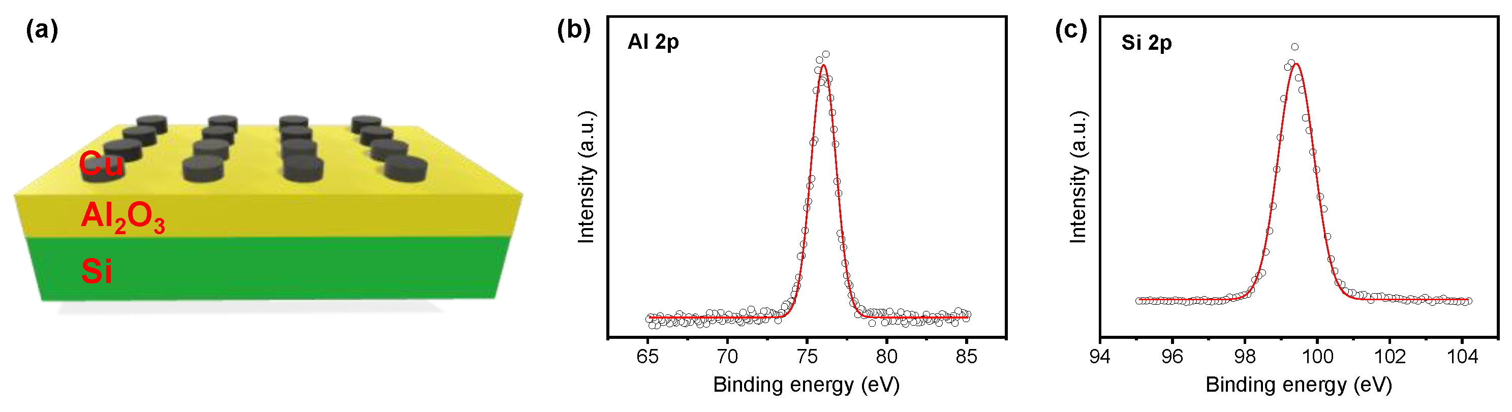
Figure 1a illustrates a schematic of the Cu/Al2O3/Si stack examined in this work. We verified the material and chemical compositions of the Al2O3/Si stack before the electrical measurement characteristics. Figure 1b,c show the XPS spectra, including raw data and fitting curves, of Al 2p and Si 2p, respectively. Al 2p was the signal detected from the Al2O3 layer and Si 2p was the signal detected from the substrate. The peak was centered at 76.05 eV in Al 2p, which corresponds to the Al-O bonds [36]. The peak of Si was centered at 99.41 eV, which indicates that the Si peak was from the Si-Si bonds [37].
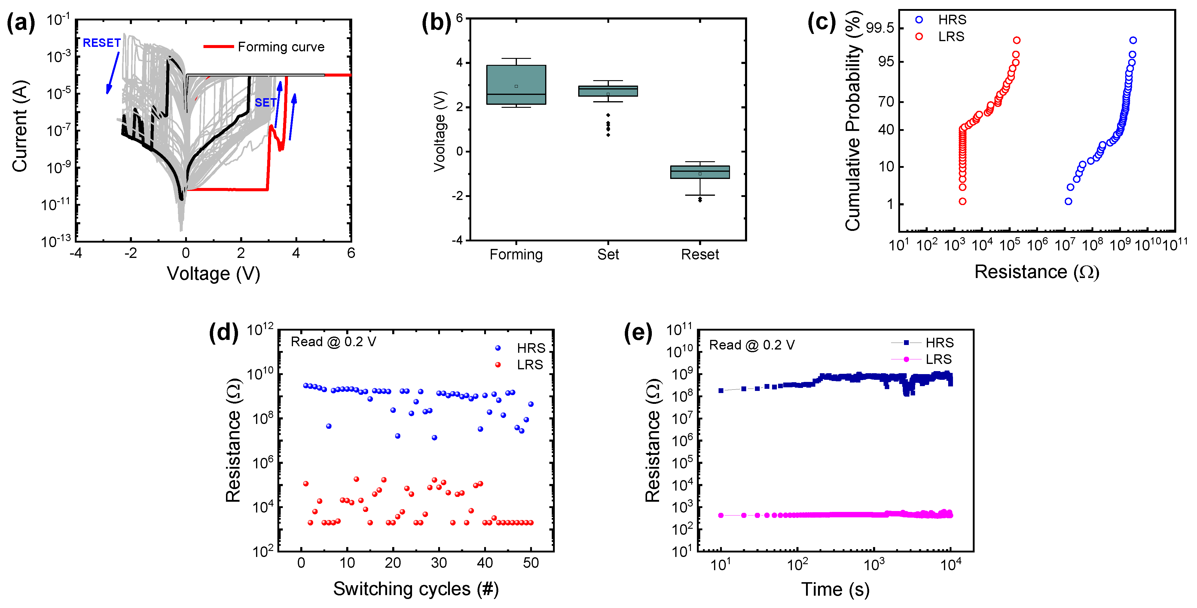
Figure 2a shows the current–voltage (I–V) characteristics, including the forming, set, and reset processes, for the Cu/Al2O3/Si device. The forming process activated the device for resistive switching. Here, the compliance current of 100 μA was used to ensure that the device was not destroyed during a current surge. The forming process induces oxygen vacancies and the Cu filament in the Al2O3 layer, resulting in a decrease in resistance. It is well known that the oxygen vacancies, as well as the Cu filament, can contribute to the increase in conductance [38].
Next, the reset process occurred with a negative bias sweep, wherein the resistance increases by reducing the oxygen vacancies and the size of the Cu filament in the insulator. Meanwhile, the set process occurred by sweeping in a positive direction to decrease the resistance again. In this way, the set and reset processes can be performed repeatedly. Figure 2b shows the statistical distribution, including the forming, set, and reset voltages. The average forming voltage of 2.95 V was slightly higher than the set voltage of 2.59 V. This is because there were few oxygen vacancies in the initial state, so achieving a soft breakdown of the device by the forming process requires a larger voltage than doing so by the set process. The average reset voltage was −0.998 V. There were also cycles in which the current was reduced by several steps. Therefore, the reset voltage is based on the point at which the first current decreased. Figure 2c shows the cumulative probability of the low-resistance state (LRS) and the high-resistance state (HRS) in the cycle-to-cycle. Variations in LRS occurred from the current overshoot during the forming and set processes. The LRS current could be controlled well even though the same compliance current was applied to the device during the cycle. Figure 2d shows the endurance cycle in which the LRS and HRS resistances were extracted at a read voltage of 0.2 V. The bouncing point did not show a certain tendency, and the LRS and HRS could be divided more than 10 times, even in the worst case. The I–V curves and endurance properties were similar in the other four cells in Figure S1. Figure 2e shows the retention properties of HRS and LRS; HRS was run for 10,000 s. HRS slightly fluctuated over time, but the on/off ratio was sufficiently maintained, indicating that the Cu/Al2O3/Si device is suitable for nonvolatile memory application.
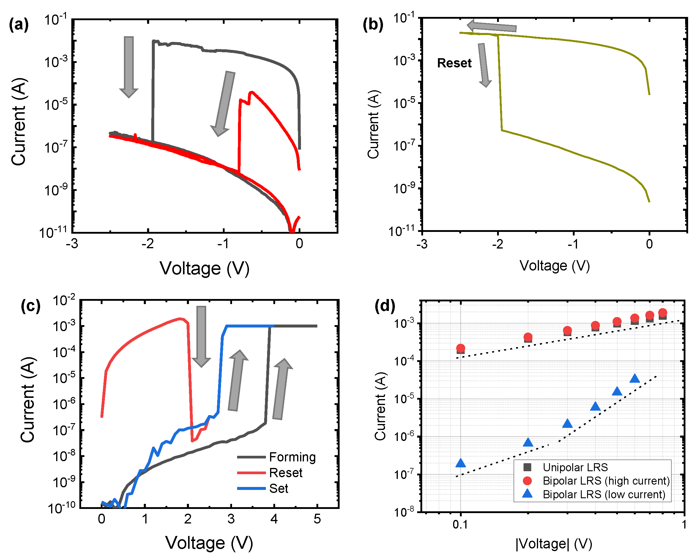
Next, we closely investigated the I–V curves for nonideal resistive switching. High-LRS currents and low-LRS currents are classified by two typical curves (Figure 3a). The high current by the current overshoot can be the nonideal case. The reset did not occur in some instances of switching, due to the overgrowth of the conducting filament caused by the Cu filament and oxygen vacancies. A reset occurred on the return sweep voltage, as shown in Figure 3b. However, if only a single sweep had been applied, the state would have been fixed at LRS. The reset process for the high current could occur by Joule heating. Figure 3c shows the unipolar switching of the Cu/Al2O3/Si device in which the set process and the reset process occurred at the same polarity, as shown in Figure 3c. The unipolar and bipolar resistive switching are both observed in Al2O3-based RRAM in the literature. The reset current in the unipolar resistive switching is higher than that in the bipolar resistive switching. Our device showed similar results [39]. The results confirm that the high LRS current in the bipolar type was similar to the LRS current in the unipolar type using log–log fitting (Figure 3d). The two cases had a similar slope of 1 following Ohmic conduction. This indicates that a strong conducting filament could be formed in the two cases. On the other hand, the low LRS current in the bipolar type had two distinctive slopes following the space-charge-limited current (SCLC) mechanism. Ohmic conduction occurs in the low-voltage regime in which thermally generated carriers are more dominant than the injected carrier. The higher voltage regime can be explained by trap-limited SCLC in which the total current is determined by the injected carriers.
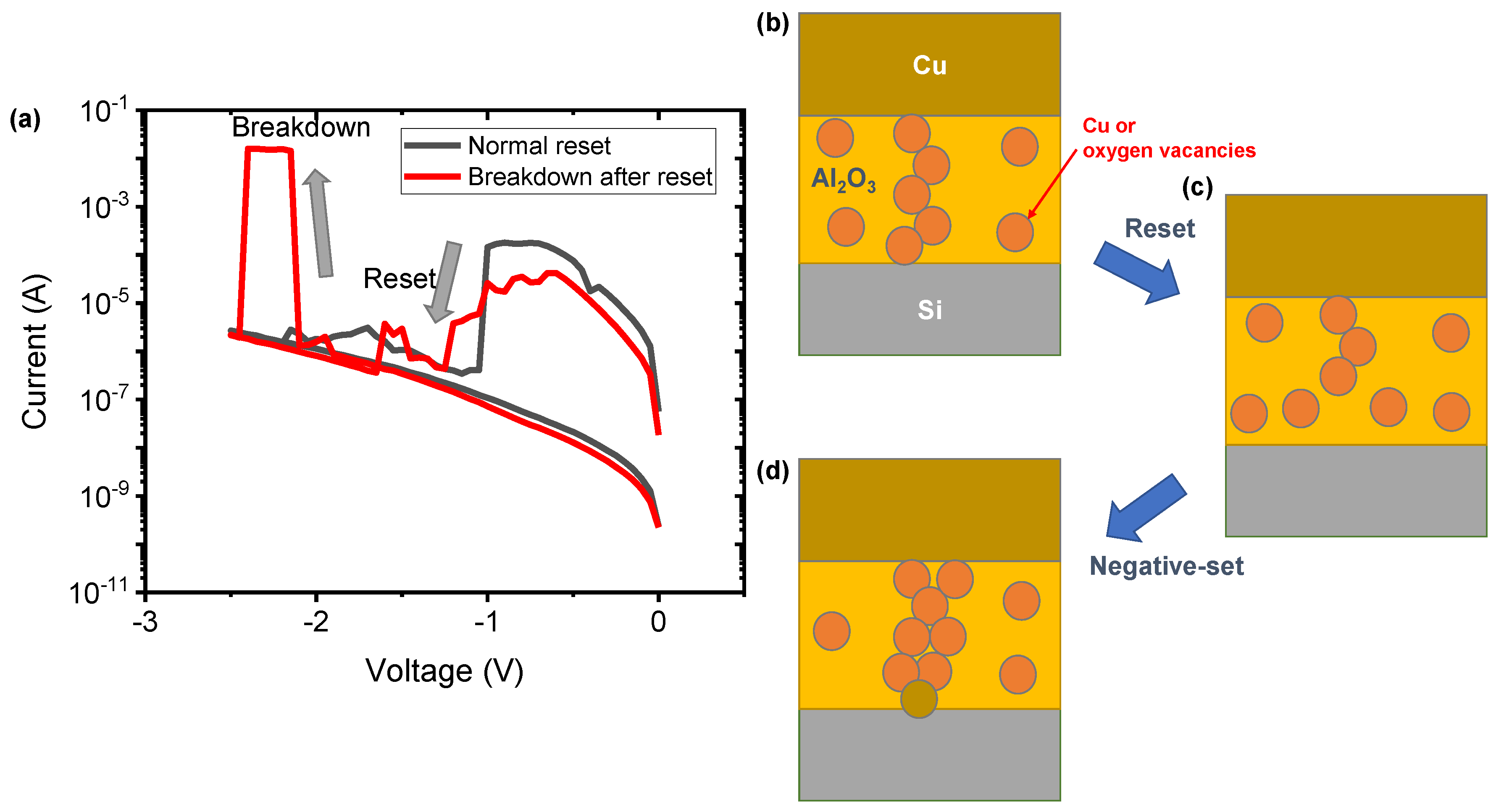
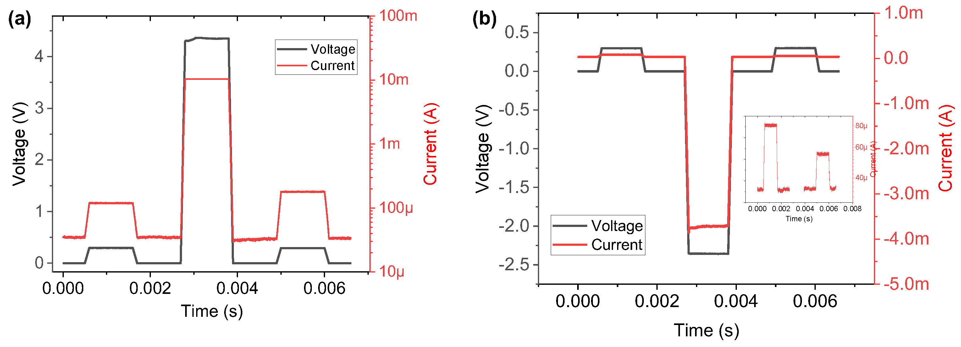
The other case of nonideal switching is negative-set behavior. Figure 4a shows I–V curves of the normal reset (black curve) and the breakdown after reset (red curve). The negative-set behavior can induce the resistive switching failure. The repeated breakdown can cause a permanent breakdown, after which it is stuck in LRS. It is impossible to return to HRS by an additional reset process after negative-set behavior. The possible filament evolution of negative-set behavior is illustrated in Figure 4b–d. LRS was completed by the set process in which the Cu filament was formed by the diffusion of Cu ions from the top electrode (Figure 4b). The conducting filament was ruptured by the reset process, causing the device to change from LRS to HRS (Figure 4c). The current increased as a result of connecting the filament from the movement of the Cu ion when a larger voltage was applied. Here, it was difficult to stop the voltage before negative-set, due to the variation in reset voltage. Similar negative-set behaviors of the conductive bridge random-access memory (CBRAM) type have been reported in the Cu/ZrO2/Pt [40] device and the Ag/ZrO2/Pt device [41]. Finally, we demonstrated the pulse operation for the set and reset processes without negative-set behavior. Figure 5a,b show the transient characteristics in a double-Y plot including voltage and current as a function of time for the set and reset processes, respectively. The set voltage, reset voltage, and read voltage were 4.5, −2.5, and 0.3 V, respectively. The current change was checked by two read pulses.
4. Conclusions
In summary, we studied the irregular resistive switching of a Cu/Al2O3/Si device, which can cause reliability issues. The Al2O3 layer and Si substrate were detected using an XPS depth profile. The cell-to-cell cycle and device-to-device characteristics were examined by scanning DC I–V curves. Due to the thin Al2O3, there was not much difference between the forming voltage and the set voltage. The variation in LRS was caused by the current overshoot in the set process. The variation in HRS occurred as a result of the uneven reset process. The LRS and HRS were maintained for 10,000 s. The uncontrolled high LRS current was similar to the LRS current in unipolar resistive switching, which was verified by the current–voltage fitting. Negative-reset behavior was confirmed, and a possible Cu filament model was presented. Finally, the increase and decrease in the current were performed by pulses without nonideal effects.
Supplementary Materials
The following are available online at https://0-www-mdpi-com.brum.beds.ac.uk/article/10.3390/met11040653/s1, Figure S1: I–V curves and endurance characteristics of different cells.
Author Contributions
H.R. conducted the electrical measurements and wrote the manuscript; S.K. designed the experiment and supervised the study. All authors have read and agreed to the published version of the manuscript.
Funding
This work was supported in part by the National Research Foundation of Korea (NRF), grant funded by the Korean government (MSIP) under Grant 2021R1C1C1004422 and by Korea Institute of Energy Technology Evaluation and Planning (KETEP) and the Ministry of Trade, Industry & Energy (MOTIE) of the Republic of Korea (no.20194030202320).
Institutional Review Board Statement
Not applicable.
Informed Consent Statement
Not applicable.
Data Availability Statement
Not applicable.
Conflicts of Interest
The authors declare no conflict of interest.
References
- Son, J.-H.; Shin, Y.-H. Direct observation of conducting filaments on resistive switching of NiO thin films. Appl. Phys. Lett. 2008, 92, 222106. [Google Scholar] [CrossRef]
- Schroeder, H.; Jeong, D.S. Resistive switching in a Pt/TiO2/Pt thin film stack–a candidate for a non-volatile ReRAM. Microelectron. Eng. 2007, 84, 1982. [Google Scholar] [CrossRef]
- Ahn, Y.; Son, J.Y. Thickness scaling effests of self-assembled NiO nanodots on resistive switching characteristics. J. Alloys Compd. 2021, 872, 159666. [Google Scholar] [CrossRef]
- Sahu, B.K.; Das, A.K.; Ajimsha, R.S.; Misra, P. Studies on transient characteristics of unipolar resistive switching processes in TiO2 thin film grown by atomic layer deposition. J. Phys. D Appl. Phys. 2018, 51, 215101. [Google Scholar] [CrossRef]
- Chen, A. Memory selector devices and crossbar array design: A modeling-based assessment. J. Comp. Electron. 2017, 16, 1982. [Google Scholar] [CrossRef]
- Park, J. Neuromorphic Computing Using Emerging Synaptic Devices: A Retrospective Summary and an Outlook. Electronics 2020, 9, 1414. [Google Scholar] [CrossRef]
- Pan, F.; Gao, S.; Chen, C.; Song, C.; Zeng, F. Recent progress in resistive random access memories: Materials, switching mechanisms, and performance. Mater. Sci. Eng. R Rep. 2014, 83, 1–59. [Google Scholar] [CrossRef]
- Maikap, S.; Banergee, W. In Quest of Nonfilamentary Switching: A Synergistic Approach of Dual Nanostructure Engineering to Improve the Variability and Reliability of Resistive Random-Access-Memory Devices. Adv. Electron. Mater. 2020, 6, 2000209. [Google Scholar] [CrossRef]
- Ryu, H.; Kim, S. Synaptic Characteristics from Homogeneous Resistive Switching in Pt/Al2O3/TiN Stack. Nanomaterials 2020, 10, 2055. [Google Scholar] [CrossRef]
- Lin, J.; Wang, S.; Liu, H. Multi-Level Switching of Al-Doped HfO2 RRAM with a Single Voltage Amplitude Set Pulse. Electronics 2021, 10, 731. [Google Scholar] [CrossRef]
- Lian, X.; Shen, X.; Fu, J.; Gao, Z.; Wan, X.; Liu, X.; Hu, E.; Xu, J.; Tong, Y. Electrical Properties and Biological Synaptic Simulation of Ag/MXene/SiO2/Pt RRAM Devices. Electronics 2020, 9, 2098. [Google Scholar] [CrossRef]
- Ryu, H.; Choi, J.; Kim, S. Voltage Amplitude-Controlled Synaptic Plasticity from Complementary Resistive Switching in Alloying HfOx with AlOx-Based RRAM. Metals 2020, 10, 1410. [Google Scholar] [CrossRef]
- Zhao, X.; Song, P.; Gai, H.; Li, Y.; Ai, C.; Wen, D. Li-Doping Effect on Characteristics of ZnO Thin Films Resistive Random Access Memory. Micromachines 2020, 11, 889. [Google Scholar] [CrossRef]
- Chen, Y.-C.; Lin, C.-C.; Chang, Y.-F. Post-Moore Memory Technology: Sneak Path Current (SPC) Phenomena on RRAM Crossbar Array and Solutions. Micromachines 2021, 12, 50. [Google Scholar] [CrossRef]
- Pérez, E.; González Ossorio, Ó.; Dueñas, S.; Castán, H.; García, H.; Wenger, C. Programming Pulse Width Assessment for Reliable and Low-Energy Endurance Performance in Al:HfO2-Based RRAM Arrays. Electronics 2020, 9, 864. [Google Scholar] [CrossRef]
- Simanjuntak, F.M.; Ohno, T.; Tseng, T.-Y. Neutral Oxygen Beam Treated ZnO-Based Resistive Switching Memory Device. ACS Appl. Electron. Mater. 2019, 1, 18. [Google Scholar] [CrossRef]
- Rajasekaran, S.; Simanjuntak, F.M.; Panda, D.; Chandrasekaran, S.; Aluguri, R.; Saleem, A.; Tseng, T.-Y. Fast, Highly Flexible, and Transparent TaOx-Based Environmentally Robust Memristors for Wearable and Aerospace Applications. ACS Appl. Electron. Mater. 2020, 2, 3131–3140. [Google Scholar] [CrossRef]
- Simanjuntak, F.M.; Chandrasekaran, S.; Lin, C.-C.; Tseng, T.-Y. Switching Failure Mechanism in Zinc Peroxide-Based Programmable Metallization Cell. Nanoscale Res. Lett. 2018, 13, 327. [Google Scholar] [CrossRef]
- Chandrasekaran, S.; Simanjuntak, F.M.; Tseng, T.-Y. Controlled resistive switching characteristics of ZrO2-based electrochemical metallization memory devices by modifying the thickness of the metal barrier layer. Jpn. J. Appl. Phys. 2018, 57, 04FE10. [Google Scholar] [CrossRef]
- Panda, D.; Simanjuntak, F.M.; Chandrasekaran, S.; Pattanayak, B.; Singh, P.; Tseng, T.-Y. Barrier Layer Induced Switching Stability in Ga:ZnO Nanorods Based Electrochemical Metallization Memory. IEEE Trans. Nanotechnol. 2020, 19, 764–768. [Google Scholar] [CrossRef]
- Jung, J.; Bae, D.; Kim, S.; Kim, H.-D. Reduced Operation Current of Oxygen-Doped ZrN Based Resistive Switching Memory Devices Fabricated by the Radio Frequency Sputtering Method. Coatings 2021, 11, 197. [Google Scholar] [CrossRef]
- Cho, H.; Kim, S. Emulation of Biological Synapse Characteristics from Cu/AlN/TiN Conductive Bridge Random Access Memory. Nanomaterials 2020, 10, 1709. [Google Scholar] [CrossRef]
- Waser, R.; Dittmann, R.; Staikov, G.; Szot, K. Redox-Based Resistive Switching Memories-Nanoionic Mechanisms, Prospects, Challenges. Adv. Mater. 2009, 21, 2632–2663. [Google Scholar] [CrossRef]
- Mikhaylov, A.; Belov, A.; Korolev, D.; Antonov, I.; Kotomina, V.; Kotina, A.; Gryaznov, E.; Sharapov, A.; Koryazhkina, M.; Kryukov, R.; et al. Multilayer Metal-Oxide Memristive Device with Stabilized Resistive Switching. Adv. Mater. Technol. 2020, 5, 1900607. [Google Scholar] [CrossRef]
- Ryu, H.; Kim, S. Self-Rectifying Resistive Switching and Short-Term Memory Characteristics in Pt/HfO2/TaOx/TiN Artificial Synaptic Device. Nanomaterials 2020, 10, 2159. [Google Scholar] [CrossRef]
- Ryu, H.; Kim, S. Pseudo-Interface Switching of a Two-Terminal TaOx/HfO2 Synaptic Device for Neuromorphic Applications. Nanomaterials 2020, 10, 1550. [Google Scholar] [CrossRef] [PubMed]
- Kim, T.H.; Nili, H.; Kim, M.H.; Min, K.K.; Park, B.G.; Kim, H. Reset-voltage-dependent precise tuning operation of TiOx/Al2O3 memristive crossbar array. Appl. Phys. Lett. 2020, 117, 152103. [Google Scholar] [CrossRef]
- Chelko, S.A.; Song, J.; Yoo, J.; Lim, S. An excellent performance of a C-Te OTS device with amorphous Ge interfacial layer for selector application. Appl. Phys. Lett. 2019, 114, 102106. [Google Scholar]
- Kim, S.; Jung, S.; Kim, M.-H.; Chen, Y.-C.; Chang, T.-C.; Ryoo, K.-C.; Cho, S.; Lee, J.-H.; Park, B.-G. Scaling Effect on Silicon Nitride Memristor with Highly Doped Si Substrate. Small 2018, 14, 1704062. [Google Scholar] [CrossRef]
- Sun, L.; Wang, W.; Yang, H. Recent Progress in Synaptic Devices Based on 2D Materials. Adv. Intell. Syst. 2020, 2, 1900167. [Google Scholar]
- Ryu, H.; Kim, S. Improved Pulse-Controlled Conductance Adjustment in Trilayer Resistors by Suppressing Current Overshoot. Nanomaterials 2020, 10, 2462. [Google Scholar] [CrossRef]
- Xia, Q.; Yang, J.J. Memristive crossbar arrays for brain-inspired computing. Nat. Mater. 2019, 18, 309–323. [Google Scholar] [CrossRef]
- Mikhaylov, A.; Pimashkin, A.; Pigareva, Y.; Gerasimova, S.; Gryaznov, E.; Shchanikov, S.; Zuev, A.; Talanov, M.; Lavrov, I.; Demin, V.; et al. Neurohybrid Memristive CMOS-Integrated Systems for Biosensors and Neuroprosthetics. Front. Mol. Neurosci. 2020, 14, 358. [Google Scholar] [CrossRef] [PubMed]
- Kim, S.; Chen, J.; Chen, Y.-C.; Kim, M.-H.; Kim, H.; Kwon, M.-W.; Hwang, S.; Ismail, M.; Li, Y.; Miao, X.-S.; et al. Neuronal dynamics in HfO x/AlO y-based homeothermic synaptic memristors with low-power and homogeneous resistive switching. Nanoscale 2019, 11, 237–245. [Google Scholar] [CrossRef] [Green Version]
- Mahata, C.; Kang, M.; Kim, S. Multi-Level Analog Resistive Switching Characteristics in Tri-Layer HfO2/Al2O3/HfO2 Based Memristor on ITO Electrode. Nanomaterials 2020, 10, 2069. [Google Scholar] [CrossRef] [PubMed]
- Sun, C.; Zeng, R.; Zhang, J.; Qiu, Z.-J.; Wu, D. Effects of UV-Ozone Treatment on Sensing Behaviours of EGFETs with Al2O3 Sensing Film. Materials 2017, 10, 1432. [Google Scholar] [CrossRef] [Green Version]
- Bywalex, R.; Karacuban, H.; Nienhaus, H.; Schulz, C.; Wiggers, H. Stabilization of mid-sized silicon nanoparticles by functionalization with acrylic acid. Nanoscale Res. Lett. 2012, 7, 76. [Google Scholar] [CrossRef] [PubMed] [Green Version]
- Luo, W.-C.; Hou, T.-H.; Lim, K.-L.; Lee, Y.-J.; Lei, T.-F. Reversible transition of resistive switching induced by oxygen-vacancy and metal filaments in HfO2. Solid-State Electron. 2013, 89, 167–170. [Google Scholar] [CrossRef]
- Wu, L.; Yu, S.; Lee, B.; Wong, P. Low-power TiN/Al2O3/Pt resistive switching device with sub-20 μA switching current and gradual resistance modulation. J. Appl. Phys. 2011, 110, 094104. [Google Scholar] [CrossRef]
- Liu, S.; Zhao, X.; Li, Q.; Li, N.; Wang, W.; Liu, Q.; Xu, H. Analysis of the Negative-SET Behaviors in Cu/ZrO2/Pt Devices. Nanoscal Res. Lett. 2016, 11, 542. [Google Scholar] [CrossRef] [Green Version]
- Liu, S.; Lu, N.; Zhao, X.; Xu, H.; Banerjee, W.; Lv, H.; Long, S.; Liu, Q.; Liu, M. Eliminating Negative-SET Behavior by Suppressing Nanofilament Overgrowth in Cation-Based Memory. Adv. Mater. 2016, 28, 10623–10629. [Google Scholar] [CrossRef] [PubMed]
Figure 1.
(a) Device schematics of Cu/Al2O3/Si device. (b) XPS Al 2p and (c) XPS Si 2p of Al2O3/Si stack.
Figure 1.
(a) Device schematics of Cu/Al2O3/Si device. (b) XPS Al 2p and (c) XPS Si 2p of Al2O3/Si stack.

Figure 2.
(a) I–V characteristics, (b) statistical distribution of forming voltage, set voltage, and reset voltage, (c) cumulative probability, (d) endurance cycle, and (e) retention of Cu/Al2O3/Si device.
Figure 2.
(a) I–V characteristics, (b) statistical distribution of forming voltage, set voltage, and reset voltage, (c) cumulative probability, (d) endurance cycle, and (e) retention of Cu/Al2O3/Si device.

Figure 3.
(a) Reset process including high-low-resistance state (LRS) current, low-LRS current, and HRS, (b) irregular reset process, (c) unipolar I–V curves including forming, set, and reset, and (d) log–log fitting of unipolar in the LRS and bipolar in the high LRS and low LRS for the Cu/Al2O3/Si device.

Figure 4.
(a) I–V curve of negative-set behavior. Illustration of filament for (b) LRS, (c) high-resistance state (HRS) by reset, and (d) set stuck by negative-set behavior.
Figure 4.
(a) I–V curve of negative-set behavior. Illustration of filament for (b) LRS, (c) high-resistance state (HRS) by reset, and (d) set stuck by negative-set behavior.

Figure 5.
Pulse transient characteristics. (a) Set process and (b) reset process.

Publisher’s Note: MDPI stays neutral with regard to jurisdictional claims in published maps and institutional affiliations. |
© 2021 by the authors. Licensee MDPI, Basel, Switzerland. This article is an open access article distributed under the terms and conditions of the Creative Commons Attribution (CC BY) license (https://creativecommons.org/licenses/by/4.0/).
Share and Cite
MDPI and ACS Style
Ryu, H.; Kim, S. Irregular Resistive Switching Behaviors of Al2O3-Based Resistor with Cu Electrode. Metals 2021, 11, 653. https://0-doi-org.brum.beds.ac.uk/10.3390/met11040653
AMA Style
Ryu H, Kim S. Irregular Resistive Switching Behaviors of Al2O3-Based Resistor with Cu Electrode. Metals. 2021; 11(4):653. https://0-doi-org.brum.beds.ac.uk/10.3390/met11040653
Chicago/Turabian StyleRyu, Hojeong, and Sungjun Kim. 2021. "Irregular Resistive Switching Behaviors of Al2O3-Based Resistor with Cu Electrode" Metals 11, no. 4: 653. https://0-doi-org.brum.beds.ac.uk/10.3390/met11040653
Note that from the first issue of 2016, this journal uses article numbers instead of page numbers. See further details here.