Tunable Broadband Solar Energy Absorber Based on Monolayer Transition Metal Dichalcogenides Materials Using Au Nanocubes

 , , and
Abstract
:
1. Introduction
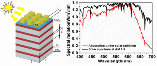
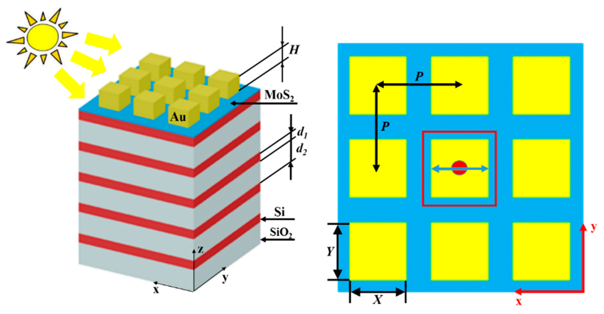
2. Structure and Theory
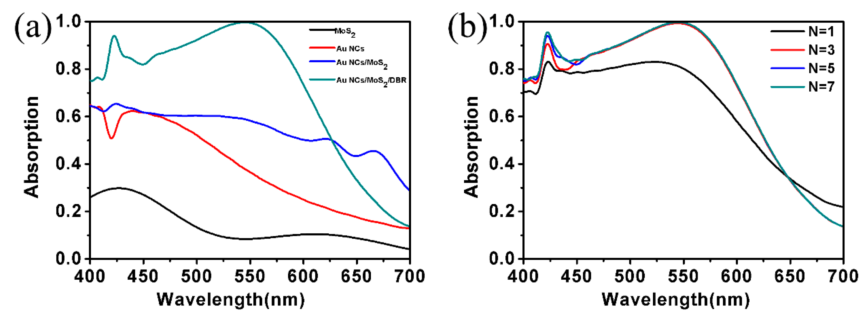
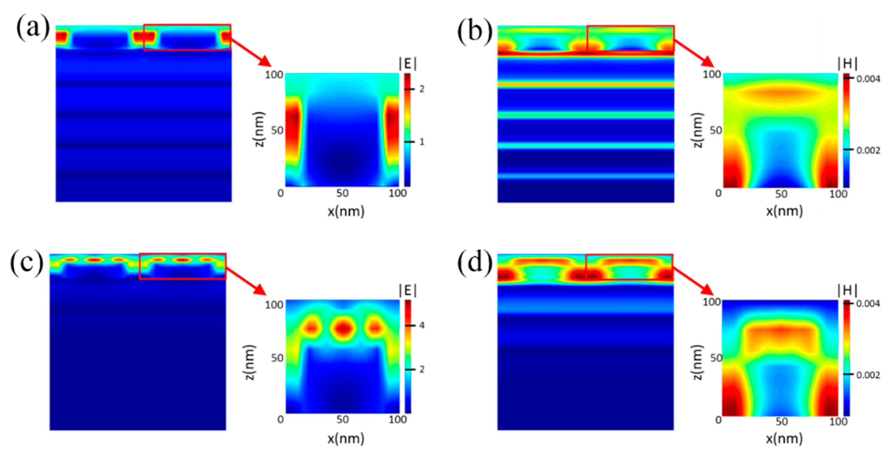
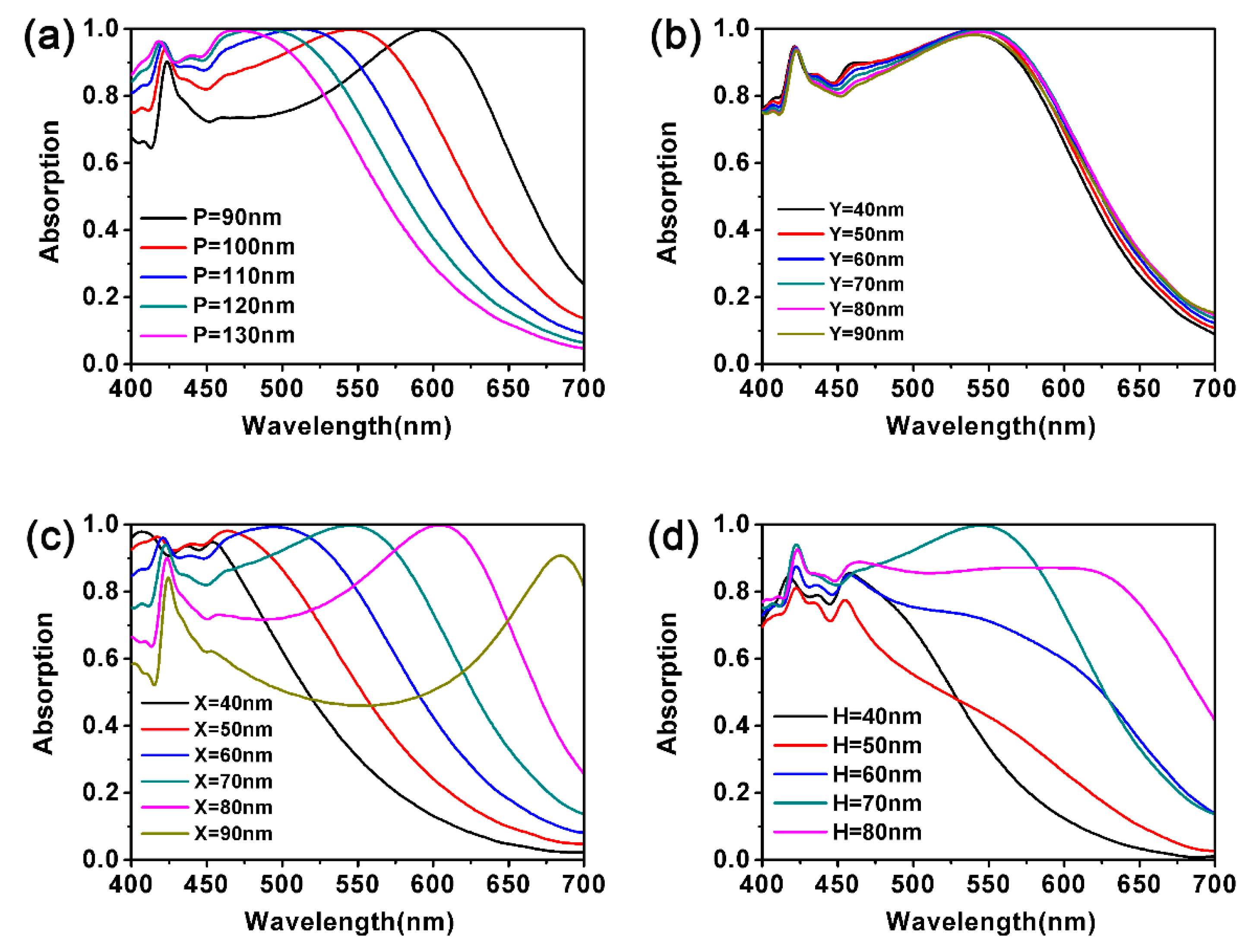
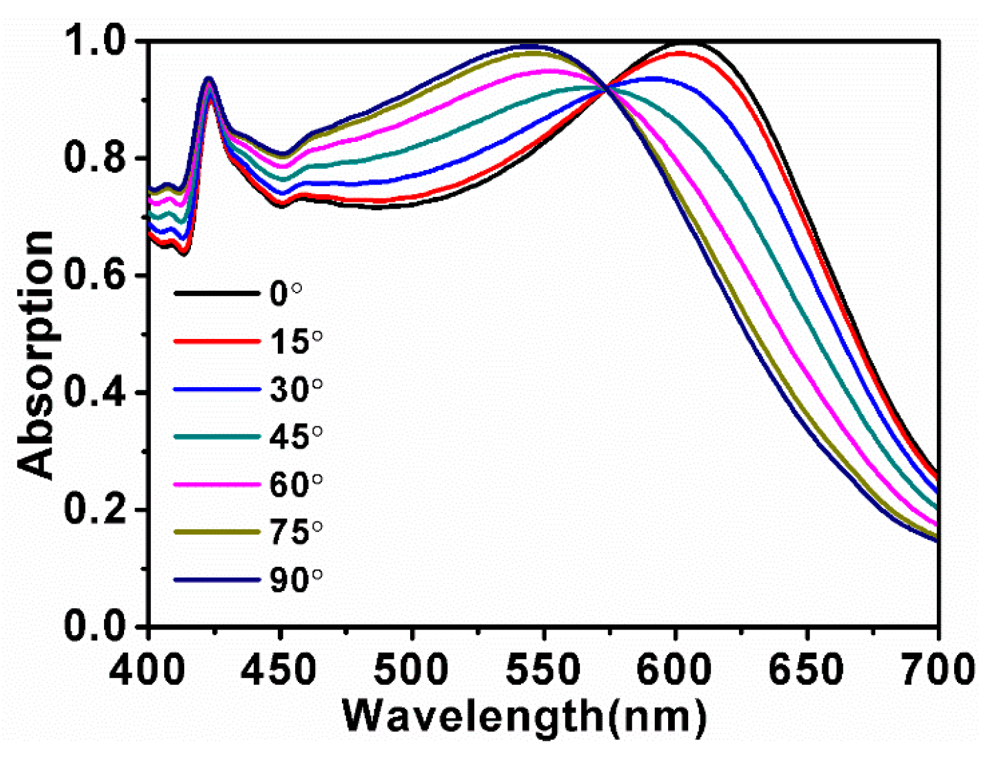
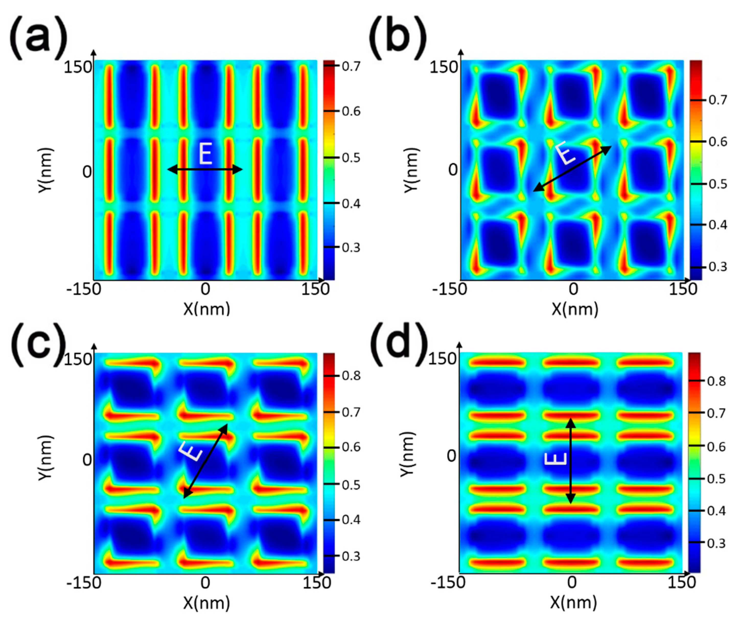
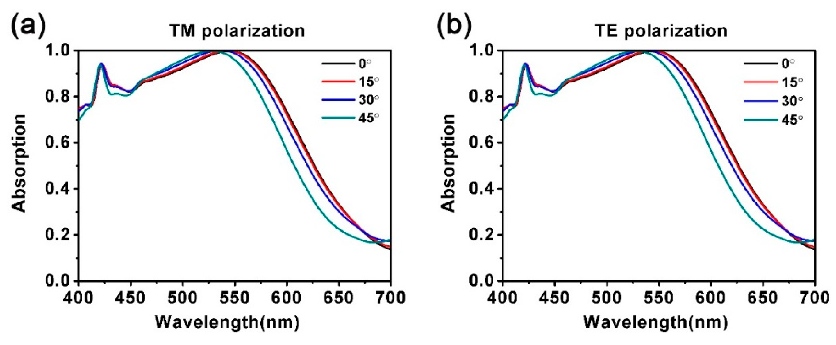
3. Results and Discussions
4. Conclusions
Author Contributions
Funding
Conflicts of Interest
References
- Liu, Z.Q.; Liu, G.Q.; Huang, Z.P.; Liu, X.S.; Fu, G.L. Ultra-broadband perfect solar absorber by an ultra-thin refractory titanium nitride meta-surface. Sol. Energy Mater. Sol. Cell. 2018, 179, 346–352. [Google Scholar] [CrossRef]
- Yu, P.Q.; Chen, X.F.; Yi, Z.; Tang, Y.J.; Yang, H.; Zhou, Z.G.; Duan, T.; Cheng, S.B.; Zhang, J.G.; Yi, Y.G. A numerical research of wideband solar absorber based on refractory metal from visible to near infrared. Opt. Mater. 2019, 97, 109400. [Google Scholar] [CrossRef]
- Liang, C.P.; Zhang, Y.B.; Yi, Z.; Chen, X.F.; Zhou, Z.G.; Yang, H.; Yi, Y.; Tang, Y.J.; Yao, W.T.; Yi, Y.G. A broadband and polarization-independent metamaterial perfect absorber with monolayer Cr and Ti elliptical disks array. Results Phys. 2019, 15, 102635. [Google Scholar] [CrossRef]
- Wu, P.H.; Chen, Z.Q.; Xu, D.Y.; Zhang, C.F.; Jian, R.H. A narrow dual-band monolayer unpatterned graphene-based perfect absorber with critical coupling in the near infrared. Micromachines 2020, 11, 58. [Google Scholar] [CrossRef] [Green Version]
- Wu, P.H.; Chen, Z.Q.; Jile, H.; Zhang, C.F.; Xu, D.Y.; Lv, L. An Infrared Perfect Absorber Based on Metal-Dielectric-Metal Multi-layer Films with Nanocircle Holes Arrays. Results Phys. 2020, 16, 102952. [Google Scholar] [CrossRef]
- Wang, Y.Y.; Chen, Z.Q.; Xu, D.Y.; Yi, Z.; Chen, X.F.; Chen, J.; Tang, Y.J.; Wu, P.H.; Li, G.F.; Yi, Y.G. Triple-band perfect metamaterial absorber with good operating angle polarization tolerance based on split ring arrays. Results Phys. 2020, 16, 102951. [Google Scholar] [CrossRef]
- Cheng, Z.Z.; Cheng, Y.Z. A multi-functional polarization convertor based on chiral metamaterial for terahertz waves. Opt. Commun. 2019, 435, 178–182. [Google Scholar] [CrossRef]
- Liu, E.; Tan, W.; Yan, B.; Xie, J.; Ge, R.; Liu, J. Broadband ultra-flattened dispersion, ultra-low confinement loss and large effective mode area in an octagonal photonic quasi-crystal fiber. J. Opt. Soc. Am. A 2018, 35, 431–436. [Google Scholar] [CrossRef]
- Cen, C.L.; Chen, Z.Q.; Xu, D.Y.; Jiang, L.Y.; Chen, X.F.; Yi, Z.; Wu, P.H.; Li, G.F.; Yi, Y.G. High quality factor, high sensitivity metamaterial graphene-perfect absorber based on critical coupling theory and impedance matching. Nanomaterials 2020, 10, 95. [Google Scholar] [CrossRef] [Green Version]
- Wang, Y.Y.; Qin, F.; Yi, Z.; Chen, X.F.; Zhou, Z.G.; Yang, H.; Liao, X.; Tang, Y.J.; Yao, W.T.; Yi, Y.G. Effect of slit width on surface plasmon resonance. Results Phys. 2019, 15, 102711. [Google Scholar] [CrossRef]
- Cen, C.L.; Zhang, Y.B.; Chen, X.F.; Yang, H.; Yi, Z.; Yao, W.T.; Tang, Y.J.; Yi, Y.G.; Wang, J.Q.; Wu, P.H. A dual-band metamaterial absorber for graphene surface plasmon resonance at terahertz frequency. Phys. E 2020, 117, 113840. [Google Scholar] [CrossRef]
- Fang, R.; Miao, C.; Mou, H.Y.; Xiao, W. Facile synthesis of Si@TiO2@rGO composite with sandwich-like nanostructure as superior performance anodes for lithium ion batteries. J. Alloys Compd. 2020, 818, 152884. [Google Scholar] [CrossRef]
- Huo, Z.; Liu, E.; Liu, J. Hollow-core photonic quasicrystal fiber with high birefringence and ultra-low nonlinearity. Chin. Opt. Lett. 2020, 18, 030603. [Google Scholar]
- Qi, Y.P.; Zhou, P.Y.; Zhang, T.; Zhang, X.W.; Wang, Y.; Liu, C.Q.; Bai, Y.L.; Wang, X.X. Theoretical study of a multichannel plasmonic waveguide notch filter with double-sided nanodisk and two slot cavities. Results Phys. 2019, 15, 102506. [Google Scholar] [CrossRef]
- Qi, Y.P.; Liu, C.Q.; Hu, B.B.; Deng, X.Y.; Wang, X.X. Tunable plasmonic absorber in THz-band range based on graphene “arrow” shaped metamaterial. Results Phys. 2019, 15, 102777. [Google Scholar] [CrossRef]
- Qi, Y.P.; Wang, Y.; Zhang, X.W.; Liu, C.Q.; Hu, B.B.; Bai, Y.L.; Wang, X.X. A theoretical study of optically enhanced transmission characteristics of subwavelength metal Y-shaped arrays and its application on refractive index sensor. Results Phys. 2019, 15, 102495. [Google Scholar] [CrossRef]
- Liu, Z.Q.; Tang, P.; Wu, B.; Shi, L.L.; Li, Y.Y.; Liu, X.S. Split graphene nano-disks with tunable, multi-band, and high-Q plasmon modes. Opt. Mater. 2019, 89, 18–24. [Google Scholar] [CrossRef]
- Liu, X.; Liu, G.; Tang, P.; Fu, G.; Du, G.; Chen, Q.; Liu, Z. Quantitatively optical and electrical-adjusting high-performance switch by grapheme plasmonic perfect absorbers. Carbon 2018, 140, 362–367. [Google Scholar] [CrossRef]
- Wang, X.X.; Wu, X.X.; Zhu, J.K.; Pang, Z.Y.; Yang, H.; Qi, Y.P. Theoretical investigation of a highly sensitive refractive-index sensor based on TM0 waveguide mode resonance excited in an asymmetric metal-cladding dielectric waveguide structure. Sensors 2019, 19, 1187. [Google Scholar] [CrossRef] [Green Version]
- Liu, C.; Yang, L.; Lu, X.L.; Liu, Q.; Wang, F.M.; Lv, J.W.; Sun, T.; Mu, H.W.; Chu, P.K. Mid-infrared surface plasmon resonance sensor based on photonic crystal fibers. Opt. Express 2017, 25, 14227–14237. [Google Scholar] [CrossRef]
- Liu, Q.; Yan, B.; Liu, J. U-shaped photonic quasi-crystal fiber sensor with high sensitivity based on surface plasmon resonance. Appl. Phys. Express 2019, 12, 052014. [Google Scholar] [CrossRef]
- Li, M.W.; Liang, C.P.; Zhang, Y.B.; Yi, Z.; Chen, X.F.; Zhou, Z.G.; Yang, H.; Tang, Y.J.; Yi, Y.G. Terahertz wideband perfect absorber based on open loop with cross nested structure. Results Phys. 2019, 15, 102603. [Google Scholar] [CrossRef]
- Cheng, Y.Z.; Fan, J.P.; Luo, H.; Chen, F. Dual-band and high-efficiency circular polarization convertor based on anisotropic metamaterial. IEEE Access 2020, 8, 7615–7621. [Google Scholar] [CrossRef]
- Cai, C.; Han, S.B.; Liu, W.; Sun, K.; Qiao, L.; Li, S.; Zu, X.T. Tuning catalytic performance by controlling reconstruction process in operando condition. Appl. Catal. B 2020, 260, 118103. [Google Scholar] [CrossRef]
- Li, W.Y.; Cheng, Y.Z. Dual-band tunable terahertz perfect metamaterial absorber based on strontium titanate (STO) resonator structure. Opt. Commun. 2020, 462, 125265. [Google Scholar] [CrossRef]
- Yan, Y.X.; Yang, H.; Yi, Z.; Xian, T. NaBH4 reduction induced evolution of Bi nanoparticles from BiOCl nanoplates and construction of promising Bi@BiOCl hybrid photocatalysts. Catalysts 2019, 9, 795. [Google Scholar] [CrossRef] [Green Version]
- Wang, Y.P.; Yang, H.; Sun, X.F.; Zhang, H.M.; Xian, T. Preparation and photocatalytic application of ternary n-BaTiO3/Ag/p-AgBr heterostructured photocatalysts for dye degradation. Mater. Res. Bull. 2020, 124, 110754. [Google Scholar] [CrossRef]
- Guan, S.T.; Yang, H.; Sun, X.F.; Xian, T. Preparation and promising application of novel LaFeO3/BiOBr heterojunction photocatalysts for photocatalytic and photo-Fenton removal of dyes. Opt. Mater. 2020, 100, 109644. [Google Scholar] [CrossRef]
- Yan, Y.X.; Yang, H.; Yi, Z.; Xian, T.; Wang, X.X. Direct Z-scheme CaTiO3@BiOBr composite photocatalysts with enhanced photodegradation of dyes. Sci. Pollut. Res. 2019, 26, 29020–29031. [Google Scholar] [CrossRef]
- Wang, Y.P.; Jiang, F.C.; Chen, J.F.; Sun, X.F.; Xian, T.; Yang, H. In situ construction of CNT/CuS hybrids and their application in photodegradation for removing organic dyes. Nanomaterials 2020, 10, 178. [Google Scholar] [CrossRef] [Green Version]
- Yan, Y.X.; Yang, H.; Yi, Z.; Li, R.S.; Xian, T. Design of ternary CaTiO3/g-C3N4/AgBr Z-scheme heterostructured photocatalysts and their application for dye photodegradation. Solid State Sci. 2020, 100, 106102. [Google Scholar] [CrossRef]
- Yi, Z.; Li, X.; Wu, H.; Chen, X.F.; Yang, H.; Tang, Y.J.; Yi, Y.G.; Wang, J.Q.; Wu, P.H. Fabrication of ZnO@Ag3PO4 Core-Shell nanocomposite arrays as photoanodes and their photoelectric properties. Nanomaterials 2019, 9, 1254. [Google Scholar] [CrossRef] [PubMed] [Green Version]
- Yi, Z.; Zeng, Y.; Wu, H.; Chen, X.F.; Fan, Y.X.; Yang, H.; Tang, Y.J.; Yi, Y.G.; Wang, J.Q.; Wu, P.H. Synthesis, surface properties, crystal structure and dye-sensitized solar cell performance of TiO2 nanotube arrays anodized under different parameters. Results Phys. 2019, 15, 102609. [Google Scholar] [CrossRef]
- Li, G.F.; Li, J.H.; Ju, Z.J.; Sun, Y.; Kong, J.Y. A novel feature extraction method for machine learning based on surface electromyography from healthy brain. Neural Comput. Appl. 2019, 31, 9013–9022. [Google Scholar] [CrossRef] [Green Version]
- Li, G.F.; Zhang, L.L.; Sun, Y.; Kong, J.Y. Towards the semg hand: Internet of things sensors and haptic feedback application. Multimed. Tools Appl. 2019, 78, 29765–29782. [Google Scholar] [CrossRef]
- Jiang, P.; Song, G.; Wang, Y.L.; Li, C.; Wang, L.L.; Yu, L. Tunable strong exciton–plasmon–exciton coupling in WS2–J-aggregates–plasmonic nanocavity. Opt. Express 2019, 27, 16613–16623. [Google Scholar] [CrossRef]
- Jiang, X.; Wang, T.; Xiao, S.; Yan, X.; Cheng, L.; Zhong, Q. Approaching perfect absorption of monolayer molybdenum disulfide at visible wavelengths using critical coupling. Nanotechnology 2018, 29, 335205. [Google Scholar] [CrossRef] [Green Version]
- Jiang, D.; Li, G.F.; Sun, Y.; Kong, J.Y.; Tao, B. Gesture recognition based on skeletonization algorithm and CNN with ASL database. Multimed. Tools Appl. 2019, 78, 29953–29970. [Google Scholar] [CrossRef]
- Li, Y.; Liu, Z.; Zhang, H.; Tang, P.; Wu, B.; Liu, G. Ultra-broadband perfect absorber utilizing refractory materials in metal-insulator composite multilayer stacks. Opt. Express 2019, 27, 11809–11818. [Google Scholar] [CrossRef]
- Chen, J.; Fan, W.F.; Zhang, T.; Chen, X.Y.; Wu, J.J.; Li, D.Y.; Yu, Y. Engineering the magnetic plasmon resonances of metamaterials for high-quality sensing. Opt. Express 2017, 25, 3675–3681. [Google Scholar] [CrossRef]
- Luo, X.; Liu, Z.M.; Cheng, Z.Q.; Liu, J.P.; Lin, Q.; Wang, L.L. Polarization-insensitive and wide-angle broadband absorption enhancement of molybdenum disulfide in the visible regime. Opt. Express 2018, 26, 33918–33929. [Google Scholar] [CrossRef] [PubMed]
- Lu, H.; Gan, X.; Mao, D.; Fan, Y.; Zhao, J. Nearly perfect absorption of light in monolayer molybdenum disulfide supported by multilayer structures. Opt. Express 2017, 25, 21630–21636. [Google Scholar] [CrossRef] [PubMed]
- Janisch, C.; Song, H.; Zhou, C.; Lin, Z. MoS2 monolayers on nanocavities: Enhancement in light–matter interaction. 2D Mater. 2016, 3, 025017. [Google Scholar] [CrossRef]
- Luo, X.; Zhai, X.; Wang, L.L.; Lin, Q. Enhanced dual-band absorption of molybdenum disulfide using a plasmonic perfect absorber. Opt. Express 2018, 26, 11658–11666. [Google Scholar] [CrossRef]
- Wang, X.X.; Zhu, J.K.; Wen, X.L.; Wu, X.X.; Wu, Y.; Su, Y.W.; Tong, H.; Qi, Y.P.; Yang, H. Wide range refractive index sensor based on a coupled structure of Au nanocubes and Au film. Opt. Mater. Express 2019, 9, 3079–3088. [Google Scholar] [CrossRef]
- Qin, F.; Chen, Z.Q.; Chen, X.F.; Yi, Z.; Yao, W.T.; Duan, T.; Wu, P.H.; Yang, H.; Li, G.F.; Yi, Y.G. A Tunable Triple-Band Near-Infrared Metamaterial Absorber Based on Au Nano-Cuboids Array. Nanomaterials 2020, 10, 207. [Google Scholar] [CrossRef] [Green Version]
- Zhou, K.; Song, J.L.; Lu, L.; Luo, Z.X.; Cheng, Q. Plasmon-enhanced broadband absorption of MoS2-based structure using Au nanoparticles. Opt. Express 2019, 27, 2305–2316. [Google Scholar] [CrossRef]
- Hou, T.; Ge, R.; Tan, W.; Liu, J. One-way rotating state of multi-periodicity frequency bands in circular photonic crystal. J. Phys. D Appl. Phys. 2020, 53, 075104. [Google Scholar] [CrossRef]
- Mehrvar, L.; Sadeghipari, M.; Tavassoli, S.; Mohajerzadeh, S.; Fathipour, M. Optical and surface enhanced Raman scattering properties of Ag modified silicon double nanocone array. Sci. Rep. 2017, 7, 12106. [Google Scholar] [CrossRef] [Green Version]
- Sobhani, A.; Lauchner, A.; Najmaei, S.; Ayala-Orozco, C.; Wen, F.; Lou, J. Enhancing the photocurrent and photoluminescence of single crystal monolayer MoS2 with resonant plasmonic nanoshells. Appl. Phys. Lett. 2014, 104, 031112. [Google Scholar] [CrossRef] [Green Version]
- Zhang, H.; Ma, Y.; Wan, Y.; Rong, X.; Xie, Z.; Wang, W. Measuring the refractive index of highly crystalline monolayer MoS2 with high confidence. Sci. Rep. 2015, 5, 8440. [Google Scholar] [CrossRef] [PubMed]
- Palik, E.D. Handbook of Optical Constants of Solids II; Academic Press: Boston, MA, USA, 1991; pp. 77–135. [Google Scholar]
- Liu, E.; Yan, B.; Tan, W.; Xie, J.; Ge, R.; Liu, J. Guiding characteristics of Sunflower-type fiber. Superlattices Microstruct. 2018, 115, 123–129. [Google Scholar] [CrossRef]
- Kou, Z.Y.; Miao, C.; Mei, P.; Zhang, Y.; Yan, X.M.; Jiang, Y.; Xiao, W. Enhancing the cycling stability of all-solid-state lithium-ion batteries assembled with Li1.3Al0.3Ti1.7(PO4)3 solid electrolytes prepared from precursor solutions with appropriate pH values. Ceram. Int. 2020. [Google Scholar] [CrossRef]
- Liu, C.; Yang, L.; Liu, Q.; Wang, F.M.; Sun, Z.J.; Sun, T.; Mu, H.W.; Chu, P.K. Analysis of a surface plasmon resonance probe based on photonic crystal fibers for low refractive index detection. Plasmonics 2018, 13, 779–784. [Google Scholar] [CrossRef]
- Shi, D.; Xiong, Z.; Li, J.; Luo, B.; Fang, L.; Xia, Y.; Gao, Z. Electron transition and electron-hole recombination processes in epitaxial BaTiO3 films with embedded Co nanocrystals. Mater. Res. Express 2019, 6, 105021. [Google Scholar] [CrossRef]
- Xiong, Z.; Cao, L. High magnetic-dielectric tunability in Ni nanocrystals embedded BaTiO3 films. J. Alloys Compd. 2019, 785, 200–205. [Google Scholar] [CrossRef]
- Qi, Y.P.; Zhang, X.W.; Zhou, P.Y.; Hu, B.B.; Wang, X.X. Refractive index sensor and filter of metal-insulator-metal waveguide based on ring resonator embedded by cross structure. Acta Phys. Sin. 2018, 67, 197301. [Google Scholar]
- Sun, J.H.; Gu, Y.J.; Lei, D.Y.; Lau, S.P.; Wong, W.T.; Wong, K.Y. Mechanistic understanding of excitation-correlated nonlinear optical properties in MoS2 nanosheets and nanodots: The role of exciton resonance. ACS Photonics 2016, 3, 2434–2444. [Google Scholar] [CrossRef]
- Wang, G.; Marie, X.; Gerber, I. Giant enhancement of the optical second-harmonic emission of WSe2 monolayers by laser excitation at exciton resonances. Phys. Rev. Lett. 2015, 114, 097403. [Google Scholar] [CrossRef] [Green Version]
- Zhang, X.W.; Qi, Y.P.; Zhou, P.Y.; Gong, H.H.; Hu, B.B.; Yan, C.M. Refractive Index Sensor Based on Fano Resonances in Plasmonic Waveguide With Dual Side-Coupled Ring Resonators. Photonic Sens. 2018, 8, 367–374. [Google Scholar] [CrossRef] [Green Version]
- Liang, C.P.; Yi, Z.; Chen, X.F.; Tang, Y.J.; Yi, Y.; Zhou, Z.G.; Wu, X.G.; Huang, Z.; Yi, Y.G.; Zhang, G.F. Dual-band infrared perfect absorber based on a Ag-dielectric-Ag multilayer films with nanoring grooves arrays. Plasmonics 2020, 15, 93–100. [Google Scholar] [CrossRef]
- Liao, M.; Wu, L.F.; Zhang, Q.B.; Dai, J.Y.; Yao, W.T. Controlled morphology of single-crystal molybdenum trioxide nanobelts for photocatalysis. J. Nanosci. Nanotechnol. 2020, 20, 1917–1921. [Google Scholar] [CrossRef] [PubMed]
- Liu, C.; Fu, G.L.; Wang, F.M.; Yi, Z.; Xu, C.H.; Yang, L.; Liu, Q.; Liu, W.; Li, X.L.; Mu, H.W.; et al. Ex-centric core photonic crystal fiber sensor with gold nanowires based on surface plasmon resonance. OPTIK 2019, 196, 163173. [Google Scholar] [CrossRef]
- Fan, J.P.; Cheng, Y.Z. Broadband high-efficiency cross-polarization conversion and multi-functional wavefront manipulation based on chiral structure metasurface for terahertz wave. J. Phys. D: Appl. Phys. 2020, 53, 025109. [Google Scholar] [CrossRef]
- He, X.K.; Sun, Z.Y.; Zou, Q.T.; Yang, J.J.; Wu, L.Y. Codeposition of nanocrystalline Co-Ni catalyst based on 1-ethyl-3-methylimidazolium bisulfate and ethylene glycol system for hydrogen evolution reaction. J. Electrochem. Soc. 2019, 166, D908–D915. [Google Scholar] [CrossRef]
- Li, R.; Miao, C.; Zhang, M.Q.; Xiao, W. Novel hierarchical structural SnS2 composite supported by biochar carbonized from chewed sugarcane as enhanced anodes for lithium ion batteries. Ionics 2019. [Google Scholar] [CrossRef]
- Zou, H.; Cheng, Y. Design of a six-band terahertz metamaterial absorber for temperature sensing application. Opt. Mater. 2019, 88, 674–679. [Google Scholar] [CrossRef]
- Marco, B.; Palummo, M.; Grossman, J.C. Extraordinary sunlight absorption and one nanometer thick photovoltaics using two-dimensional monolayer materials. Nano Lett. 2013, 13, 3664–3670. [Google Scholar]
- Mukherjee, B.; Guchhait, A.; Chan, Y.; Simsek, E. Absorptance of PbS quantum dots thin film deposited on trilayer MoS2. Adv. Mater. Lett. 2015, 6, 936–940. [Google Scholar] [CrossRef] [Green Version]
- Liu, J.; Cao, Y.; Tong, H.; Wang, D.; Wu, Z. Broad-spectrum enhanced absorption of graphene-molybdenum disulfide photovoltaic cells in metal-mirror microcavity. Nanotechnology 2018, 29, 144001. [Google Scholar]


| Absorber | Average Absorption (%) | Operating Region(nm) |
|---|---|---|
| Graphene/MoS2 Interface [69] | 15.4% | Absorption is always less than 75% |
| QDs/MoS2/SiO2/Si [70] | 22.3% | Absorption is always less than 75% |
| Monolayer MoS2 with MIM [44] | Less than 50% | 500–750 |
| GM-PVc in w-MMCs [71] | 65% | 450–700 |
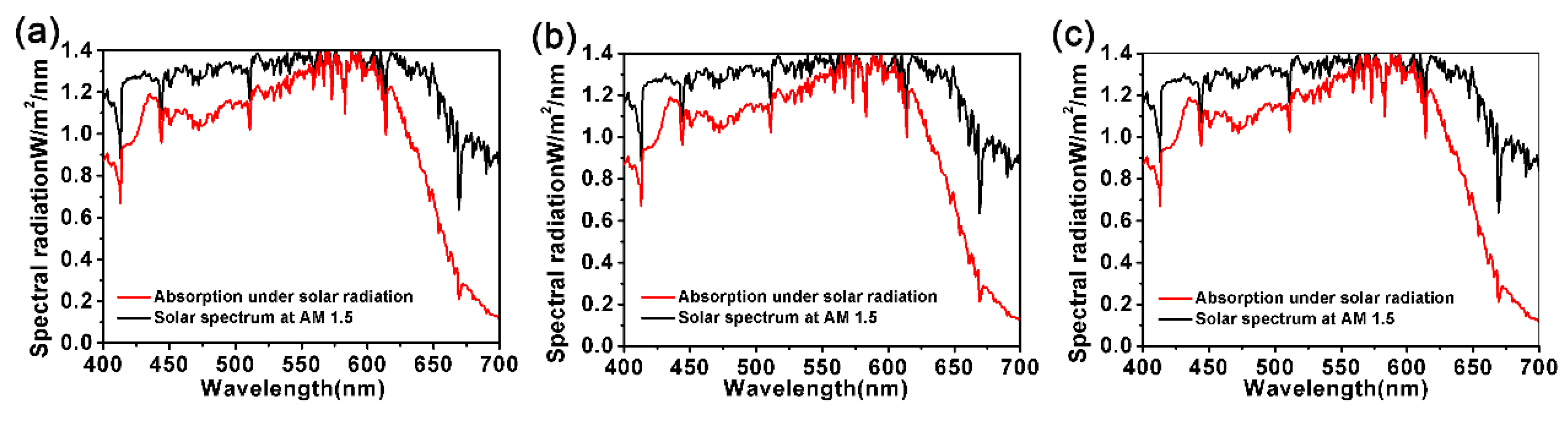
| Proposed (monolayer MoS2/Au NCs/DBR) | 77.3% | 400–700, absorbance is more than 90.4% from 430 to 630 nm |
© 2020 by the authors. Licensee MDPI, Basel, Switzerland. This article is an open access article distributed under the terms and conditions of the Creative Commons Attribution (CC BY) license (http://creativecommons.org/licenses/by/4.0/).
Share and Cite
Li, J.; Chen, Z.; Yang, H.; Yi, Z.; Chen, X.; Yao, W.; Duan, T.; Wu, P.; Li, G.; Yi, Y. Tunable Broadband Solar Energy Absorber Based on Monolayer Transition Metal Dichalcogenides Materials Using Au Nanocubes. Nanomaterials 2020, 10, 257. https://0-doi-org.brum.beds.ac.uk/10.3390/nano10020257
Li J, Chen Z, Yang H, Yi Z, Chen X, Yao W, Duan T, Wu P, Li G, Yi Y. Tunable Broadband Solar Energy Absorber Based on Monolayer Transition Metal Dichalcogenides Materials Using Au Nanocubes. Nanomaterials. 2020; 10(2):257. https://0-doi-org.brum.beds.ac.uk/10.3390/nano10020257
Chicago/Turabian StyleLi, Jiakun, Zeqiang Chen, Hua Yang, Zao Yi, Xifang Chen, Weitang Yao, Tao Duan, Pinghui Wu, Gongfa Li, and Yougen Yi. 2020. "Tunable Broadband Solar Energy Absorber Based on Monolayer Transition Metal Dichalcogenides Materials Using Au Nanocubes" Nanomaterials 10, no. 2: 257. https://0-doi-org.brum.beds.ac.uk/10.3390/nano10020257