Photo-Induced Black Phase Stabilization of CsPbI3 QDs Films
by
 , and
, and
Eider A. Erazo
1,2 ,
,
H.E. Sánchez-Godoy
1,3,
Andrés F. Gualdrón-Reyes
1,
Sofia Masi
1,* and
Iván Mora-Seró
1,* 1
Institute of Advanced Materials (INAM), Universitat Jaume I (UJI), Avenida de Vicent Sos Baynat, s/n, 12071 Castellón de la Plana, Spain
2
Departamento de Química, Universidad de los Andes, Bogotá D.C. 111711, Colombia
3
Centro Universitario de los Lagos, Universidad de Guadalajara, Lagos de Moreno, Jalisco C.P. 47460, Mexico
*
Authors to whom correspondence should be addressed.
Nanomaterials 2020, 10(8), 1586; https://0-doi-org.brum.beds.ac.uk/10.3390/nano10081586
Submission received: 10 July 2020
/
Revised: 4 August 2020
/
Accepted: 10 August 2020
/
Published: 12 August 2020
(This article belongs to the Special Issue Low-Dimensional Perovskites: From Materials Design to Optoelectronic Devices)
Abstract
:α-CsPbI3 quantum dots (QDs) show outstanding photoelectrical properties that had been harnessed in the fabrication of perovskite QDs solar cells. Nevertheless, the stabilization of the CsPbI3 perovskite cubic phase remains a challenge due to its own thermodynamic and the presence of surface defects. Herein, we report the optimization of the CsPbI3 QDs solar cells, by monitoring the structure, the morphology and the optoelectronic properties after a precise treatment, consisting of the conventional solvent washing with a time limited ultraviolet (UV) exposure combination, during the layer-by-layer deposition. The UV treatment compensates the defects coming from the essential but deleterious washing treatment. The material is stable for 200 h and the PCE improved by the 25% compared with that of the device without UV treatment. The photo-enhanced ion mobility mechanism is discussed as the main process for the CsPbI3 QDs and solar cell stability.
1. Introduction
Perovskite solar cells are the most promising next generation photovoltaic technologies to produce solar energy with very high efficiency [1]. Currently, the main limitation is the perovskite low stability in ambient conditions [2]. The halide ABX3 perovskite materials are based on two cations, A (formamidinium, methylammonium, and Cs), a metallic one B (Pb2+, Sn2+), and the halide X (I−, Br−, Cl−) [3], where the a priori most stable perovskite, with a suitable band gap (1.73 eV) [4] for photovoltaic application, is CsPbI3 due to its inorganic nature. The polymorphic behavior of the perovskite causes the thermodynamic instability of the perovskite that is characterized by a black α-phase, with a cubic or tetragonal crystal structure, predominant only at high temperature [2]. Otherwise it converts in a non-perovskite yellow δ-phase, with an orthorhombic crystal structure. An effective approach to increase the α-phase stability is the manipulation of the dimensionality, moving from the 3D (bulk material) to the quantum dots (QDs) [2,5], with higher phase stability than the bulk counterpart, mainly due to the increase of the surface energy. Perovskite QDs used as active materials in a solar cell led to a photoconversion efficiency (PCE) similar to the one obtained with the bulk perovskite, 16.6%; it has been achieved with a mixed perovskite Cs1−xFAxPbI3 QDs [6], with the benefit that the low dimensionality and the combination of the two cations (cesium and formamidinium) for tuning the tolerance factor, definitively improve the stability in air [7]. Perovskite QDs present very high photoluminescence quantum yield (PLQY) indicating a reduced non-radiative recombination, allowing very high open circuit voltage (Voc) [8]. The reduced phase segregation in mixed halide perovskite nanoparticles allows for the real tuning of the perovskite bandgap with important implications for the development of tandem devices [9,10,11,12].
To take advantage of these properties for the development of perovskite quantum dots (QDs) solar cells (PQDSCs), a proper QDs coupling is needed to obtain good transport properties in QDs thin films, with a good carrier collection efficiency, essential for a working device [8]. In order to get it, a fraction of organic capping ligand, covering the colloidal QDs surface has to be removed by specific treatments. This strategy allows for closer QDs and improved transport properties of the QDs thin film. Thus, these treatments lead to two important consequences: i) the reduction of the spatial distance between the QDs and in turn the improving of the electronic coupling; ii) after removing the ligand, the QDs are not more soluble in the original solvent (i.e., octane) and another layer can be deposited on the top. It makes make possible the preparation of thicker films, necessary to increase the light absorption. Repeating the deposition-treatment steps, thicker films can be obtained by a layer-by-layer deposition, allowing for thickness control and for preparing mixed material films, stacking different types of perovskite QDs [13].
The solvent choice used to remove the ligand and improve the QD-to-QD coupling is limited to an organic non hydrogenated solvent, such as methylacetate or ethylacetate, due to the chemical compatibility with the oleate ligand and to the requirement of preserving the perovskite material itself. During this step, a ligand exchange mechanism establishes the replacement of the oleate ligand by acetic acid, resulted from the hydrolysis of methyl/ethyl acetate in air, releasing the free oleic acid [12,14]. Moreover, it has been demonstrated that this step has a huge potential, since this strategy mediates the passivation of vacancies [14], and increases the stability of the CsPbI3 when the effect of these solvents is aided by additives or additional treatments [11]. For instance, after the addition of an organic molecule such as the phenylethylammonium iodide (PEAI), the additive remains outside of the perovskite structure and the optical properties of the CsPbI3 are preserved. The PCE of solar cells by using this method is about 6%, stable for 4 months, demonstrating that the synergistic control of the surface energy and the surface functionalization has an important role in exceeding the stabilization limit [15]. Despite the effectiveness of the method, the presence of organic molecules in the active layer, that are soluble in the common solvent used for the deposition of the hole transporting material (HTM) (i.e., the chlorobenzene) could lead to an infiltration inconvenience. So far, this problem limits the performances due interface losses or more drastically, for the complete bleaching of the affected perovskite. Another approach, avoiding the use of organic additives, is the optimization of the bottom interface. The treatment with inorganic salts of the bottom layer (i.e., the mesoporous TiO2) leads to promising results, as the PCE increased from 5.58% to 14.3%, being stable for 100 h [4,5,8,16,17]. Despite the high PCE, the CsPbI3 QDs solar cells generally are fabricated with a planar architecture, as it turns out to be highly challenging to homogeneously incorporate QDs into the mesoporous structure. At the same time, this approach is difficult to replicate in planar solar cells, since the mesoporous titania is more prone to the infiltration of the chemicals and salts used in this strategy. In planar solar cells architecture, the efficiency exceeded over 14%, with a stability of almost 10 days if the QDs are passivated with a treatment with glycine [18]. Therefore, there is a lack of strategies that limit the use of chemicals and solvents to improve the CsPbI3 stability, preserving the efficiency and making it easy to reproduce regardless of the structure used.
In this work, the combined use of solvent and controlled UV treatment is reported. The choice lies in the need of, firstly, removing the ligand in excess and guarantee the QD-to-QD electronic coupling, and secondly, improving the stability of the perovskite to prepare also a material not affected by the further deposition steps. The process combines the desired desorption of the surface ligands and the ion migration, which facilitate the passivation of surface vacancies and improve the stability. Previous reports show that moderate UV light (lamp power 7 W, λ = 365 nm) promotes the oriented attachment of CsPbI3 QDs to form large nanoparticles (40 nm) along (110) facets. On the other hand, a higher UV power (lamp power 100 W, λ = 365 nm) induces the degradation of the α-CsPbI3 QDs into photoinactive δ-phase and finally into the precursors [19]. The photo-induced attachment has also been proven in CsPbBr3 nanoplatelets and nanocubes [20]. Since CsPbBr3 is more stable than CsPbI3 [21], the latter would require less energy to undergo this process, thus avoiding degradation phenomena. It is worth to note that in systems like CdSe nanoplatelets, light-induced attachment even at 1 W cm−2 is not experimented, since its covalent nature present negligible ion mobility [22]. Pointing out that the ion mobility and the presence of vacancies formed after the deposition process and washing treatment are fundamental for the success of the UV treatment. Finally, with this dry approach we obtained more stable materials and solar cells in air, with an increased efficiency up to 7.4%, due, at the same time, to the improved optoelectronic properties and to the interface structural quality, taking advantage from the own photoactivity of the perovskite.
2. Materials and Methods
2.1. Synthesis of CsPbI3 QDs
All the purchased chemicals were used as received. CsPbI3 QDs were synthesized according to the hot-injection method described elsewhere [7], by mixing stoichiometrically Cs-oleate and lead iodide (PbI2, AB111058, 99.999%, acbr GmbH, Karlsruhe, Germany. Cs-oleate was first prepared by mixing 0.610 g Cs2CO3 (202126, 99.9%, Sigma-Aldrich, Madrid, Spain), 2.5 mL oleic acid (OA, 364525, 90%, Sigma-Aldrich, Madrid, Spain), and 30 mL of 1-octadecene (ODE, O806, 90%, Sigma-Aldrich, Madrid, Spain) into a 50 mL-three neck flask for 90 min under vacuum. Then, the temperature was increased to 150 °C under N2-atmosphere to reach the complete Cs2CO3 dissolution. For the injection step, Cs-oleate was kept at 120 °C under N2-purge. Then, 1 g PbI2 and 50 mL ODE were mixed into a 100 mL-three neck flask at 120 °C under vacuum and vigorous stirring for 1 h. A preheated mixture of oleylamine (OLA, HT-OA100, 98%, Sigma-Aldrich, Madrid, Spain) and OA (5 mL each one into a beaker at 130 °C for 30 min) was added under N2-purge and temperature was rapidly raised up to reach 170 °C. In this point, preheated Cs-oleate (4 mL) was immediately injected, observing a luminescent red colloidal solution. For the purification step, 60 mL of methyl acetate (MeOAc, 296996, 99.5%, Sigma-Aldrich, Madrid, Spain) with 32 mL of liquor solution are centrifuged at 4700 RPM for 5 min. The precipitated QDs were recovered from supernatant and re-dispersed in 5 mL of hexane (CHROMASOLV, 34859, 99.7%, Honeywell, Barcelona, Spain). A second purification was conducted by adding 5 mL of MeOAc to the QDs dispersion and centrifuged at 4700 RPM for 5 min. The QDs product was obtained and re-dispersed with 10 mL of hexane. The final colloidal solution was stored in the fridge at least for 24 h before use it.
2.2. Quantum Dot Solution Preparation
A prepared solution of CsPbI3 QDs in hexane was stored at 4 °C into a fridge. After 1 day, the supernatant was taken out and centrifuged at 6500 rpm for 10 min. After drying the new supernatant with nitrogen flow, a proper amount of octane was added to obtain 70 mg/mL.
2.3. Solar Cell Fabrication
Metallic zinc powder was used for etching with 6 M HCl. Subsequently, Indium-tin-oxide (ITO) substrates were brushed and then sequentially sonicated in soapy water, milliQ water, acetone, and isopropanol (15 min each solvent). Substrates were dried with an air gun. For the tin oxide layer deposition, the substrates were treated in UV–ozone for 20 min, then 110 µL of 2.6% v/v SnO2 solution diluted from a 15% tin (IV) oxide colloidal solution (Alfa Aesar, Barcelona, Spain) were spin coated during 40 s at 3000 RPM. Before the annealing for 30 min at 150 °C in a hot plate, one side of the substrates was cleaned with a wet cotton swap around 5 mm to ensure the contact with the gold electrode.
The solar cells were fabricated inside a nitrogen filled glove box with O2 and H2O level lower than 5 ppm. To deposit the absorber layer, the ITO/SnO2 substrates were treated by UV-ozone during 60 min, then 20 µL of 70 mg/mL CsPbI3 QDs in octane were spin coated according to the following program: 1 s to reach 1000 RPM, 20 s at 1000 RPM, 1 s to reach 2000 RPM, 85 s at 2000 RPM, and stops in 1 s. Then, 300 µL of ethyl acetate were quickly added when the spin reach 2000 RPM. For the devices treated with UV, every layer after the ethyl acetate washing was put under UV light (ELC 500 UV cure chamber, 9 W UV lamp optical) for 2 and 4 min (this process was also conducted inside the glovebox). This process was repeated to obtain layer by layer the desired thickness of the final film. 2,2′,7,7′-Tetrakis[N,N-di(4-methoxyphenyl)amino]-9,9′-spirobifluorene (Spiro-OMeTAD) was spin coated on top of the perovskite QDs from a fresh Spiro-OMeTAD (Feming) solution according the literature [23]. Finally, 80 nm of gold contacts were thermally evaporated.
2.4. Photoelectric Characterization
The photovoltaic devices were characterized using an Abett Solar simulator equipped with an AM 1.5 filter. The light intensity was adjusted to 100 mW cm−2 using a calibrated Si photodiode (Hamamatsu S1133). The active area of the cell is 0.121 cm2, determined with a metallic external mask. All the J–V measurements were carried out after leaving the devices 1 min under 1 sun illumination in air at a temperature around 25 °C and a relative humidity around 50%, without encapsulation. Each curve was generated using 123 data points from a starting potential of 1.2 V to a final potential of −0.05 V (reverse scan) using a scan rate of 10 mVs−1. From the curves were calculated parameters like, the photoconversion efficiency (PCE), the short circuit current density (Jsc), the maximum current produced for the device when there is no external bias opposing the electrons flow (V = 0), the open circuit voltage (Voc), the maximum voltage produced by the cell which can be rationalized as the opposing voltage needed to stop the electrons flow (Jsc = 0 mA/cm2), and the fill factor (FF), determined as the ratio of the maximum power density produced to the product of Voc and Jsc of the solar cell. The incident photons to current efficiency (IPCE) measurements of the encapsulated devices are performed with a QEPVSI-b Oriel measurement system.
2.5. Structural Characterization
The morphologies of the samples (ITO/SnO2/CsPbI3) were carried out with a field emission scanning electron microscope (FEG-SEM) JEOL 3100F) operated at 5 kV. Fourier-transform infrared (FTIR) spectra are collected with a FTIR Equinox 55 (Bruker) with an ATR Pro (Jasco) equipped with a diamond crystal, in standard conditions (in the range 600–4000 cm−1). Transmission electron microscopy (TEM) images were taken on W JEOL JEM 1010 transmission electron microscope (Akishima, Tokyo, Japan), using an accelerating voltage of 100 kV, with a resolution of 0.4 nm. The X-ray diffraction (XRD) patterns of the CsPbI3 films were recorded using an X-ray diffractometer (D8 Advance, Bruker AXS, Karlsruhe, Germany) (Cu Kα, the wavelength of λ = 1.5406 Å) within the range of 5–80°.
2.6. Optical Characterization
The steady state absorption spectra of the perovskite films on glass substrate were achieved by using a UV/Vis absorption spectrophotometer (Varian, Cary 300, Palo Alto, USA), the wavelength range for the measurements was 400–800 nm. The emission measurements (steady state photoluminescence and time resolve photoluminescence) were collected by a Horiba Fluorolog Photoluminescence (PL) and measurements were conducted at an excitation of 532 nm. Since the absorbance at the excitation wavelength was not the same, to make a fair comparison the PL emission was normalized dividing by (1−10−Abs), which is usually used to compare quantum yields. All measurements were carried out under ambient conditions.
3. Results and Discussion
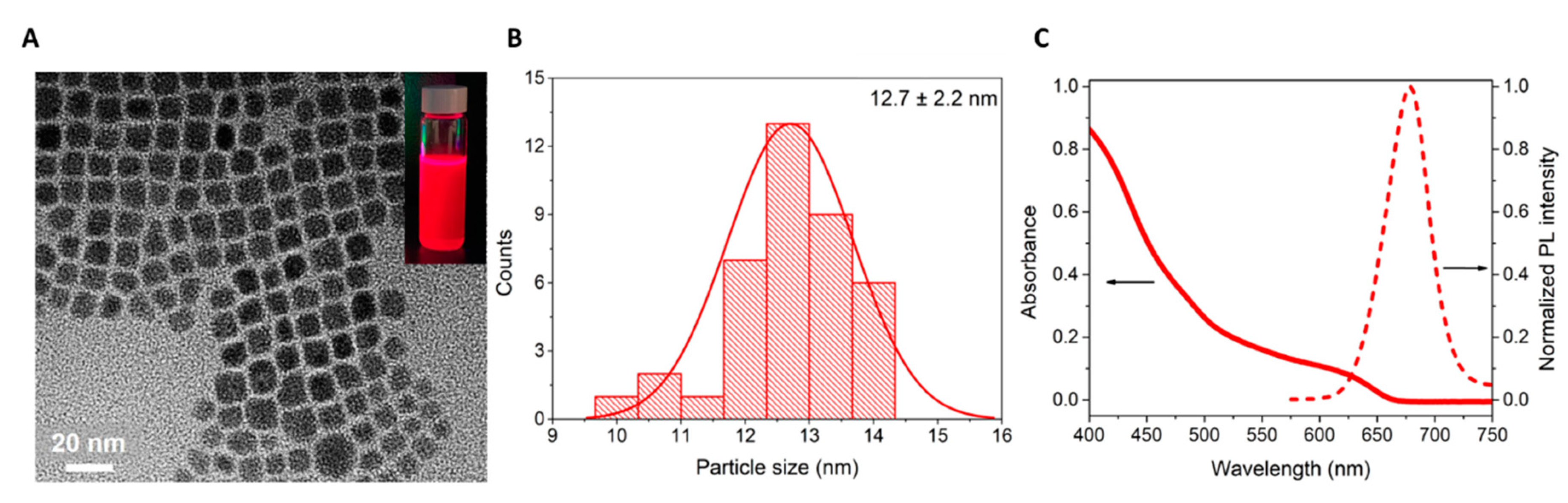
The CsPbI3 QDs used for the preparation of PQDSCs show a nanocube shape, with a size distribution of 12.7 ± 2.2 nm, see Figure 1a,b. The optical properties reveal an emission at 680 nm, see Figure 1c, and a PLQY of 94% and 82% after the first and second purification steps, respectively.
The deposition of the CsPbI3 QDs colloidal solution dispersed in octane, is preliminary optimized to remove the excess of organic ligand coming from the synthesis, by selecting between the methyl acetate and ethyl acetate and by choosing the right volume needed to deposit a second layer without washing the first one (see experimental section) [14]. The CsPbI3 film is used as active layer in PQDSCs (ITO/SnO2/CsPbI3/Spiro-OMeTAD/Au), see Figure 2a, made by depositing layer by layer 3, 5, 7, and 10 layers of QDs. With the aim of depositing one layer on the top of the other, the solvent washing treatment is vital, using EtOAc in our case. In this context, the QDs become insoluble in the solvent in which they are well dispersed (octane) because of the presence of the organic capping ligand. Then, the screening on the thickness is carried out. The photovoltaic parameters of the prepared cells are depicted in Figure 2b–e. The highest photocurrent densities, Jsc, are achieved with 3 and 5 layers, see Figure 2c. The maximum obtained Voc and fill factor (FF) are almost the same, see Figure 2d,e, respectively. Jsc slightly decreases from 3 to 5 layers, see Table 1, while for higher number of layers (7) there is an evident drop in the current, likely due to transport limitations as carriers have to travel longer distances, originated by the residual organic ligand. However, losses at the interfaces or in the bulk, which is associated to the existence of structural defects and inhomogeneity when the thickness is higher, see below, could also contribute to the performance reduction for the thicker layers prepared.
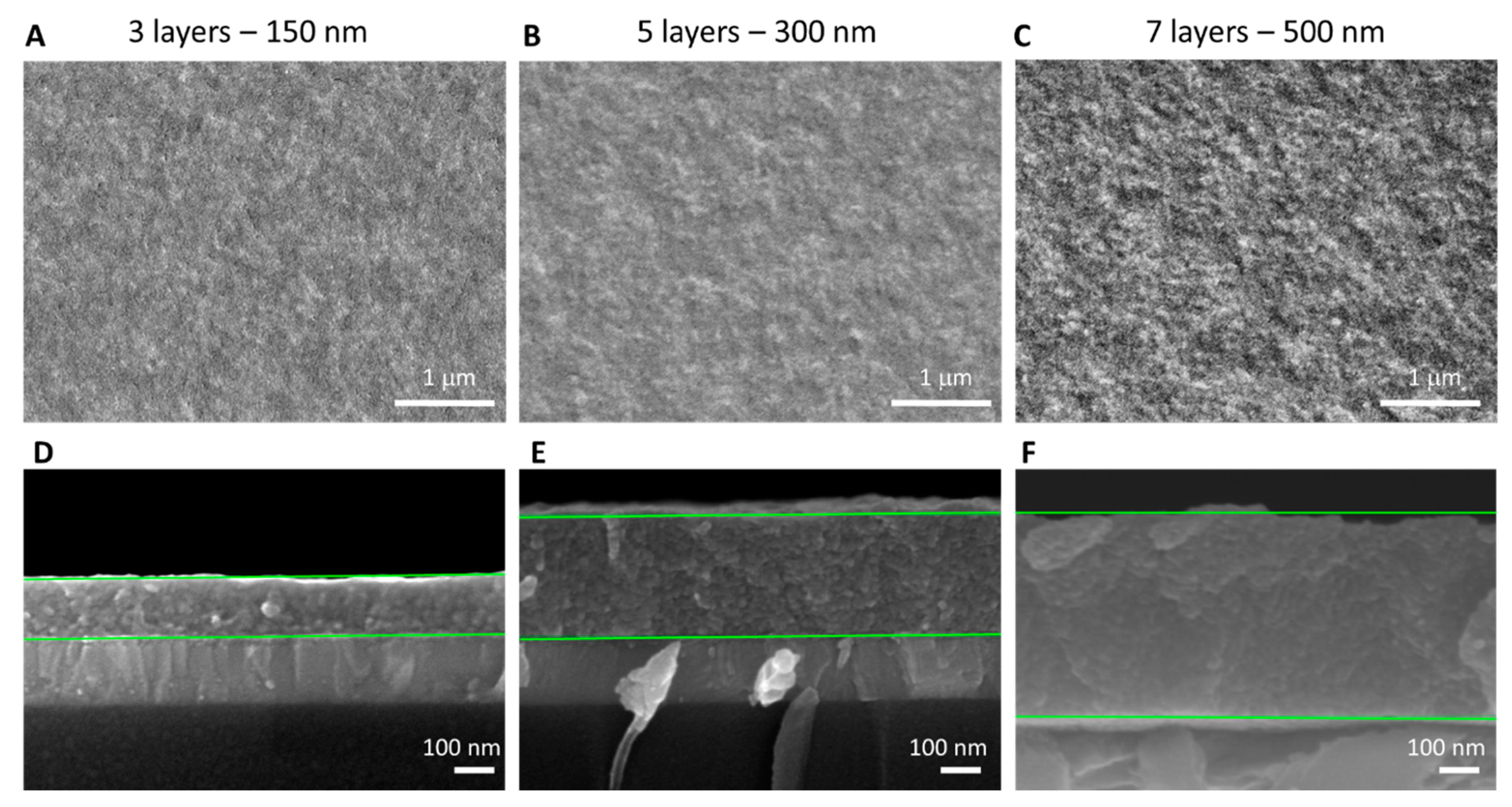
The top-view SEM images of the CsPbI3 QDs films made of 3, 5, and 7 layers, see Figure 3a–c, respectively, show very similar morphologies, although a minor difference can be noticed for the 7 layers film, Figure 3c, as it seems that relatively small and bright aggregations exist. This fact agrees with the wavy surface observed through the cross-section SEM profile, Figure 3f. In Figure S1, a higher magnification shows the film consisting of closely packed assemblies of discrete QDs, indicating that the QDs film morphology is preserved after each EtOAc washing. From the cross section SEM images, the films thicknesses of 3 and 5 layers were estimated to be 150 nm and 300 nm, respectively, which is in line with the thickness range, between 100–400 nm commonly used in CsPbI3 QDs solar cells [4,13]. On the other hand, the 7 layers film has a thickness around 500 nm. All these evidences fully explained the PCE trend by changing the thickness of the active layer. In particular, with 7 layers the surface is undulating and presents small aggregations, see Figure 3c,f, leading to not homogeneous deposition of the Spiro-OMeTAD on the top. The higher light harvesting in a thicker film cannot compensate the deleterious transport and defects, and the Jsc obtained is even lower than that of the device with 3 layers, see Figure 2c. Moreover, in line with this observation, the FF also decreases, see Figure 2e.
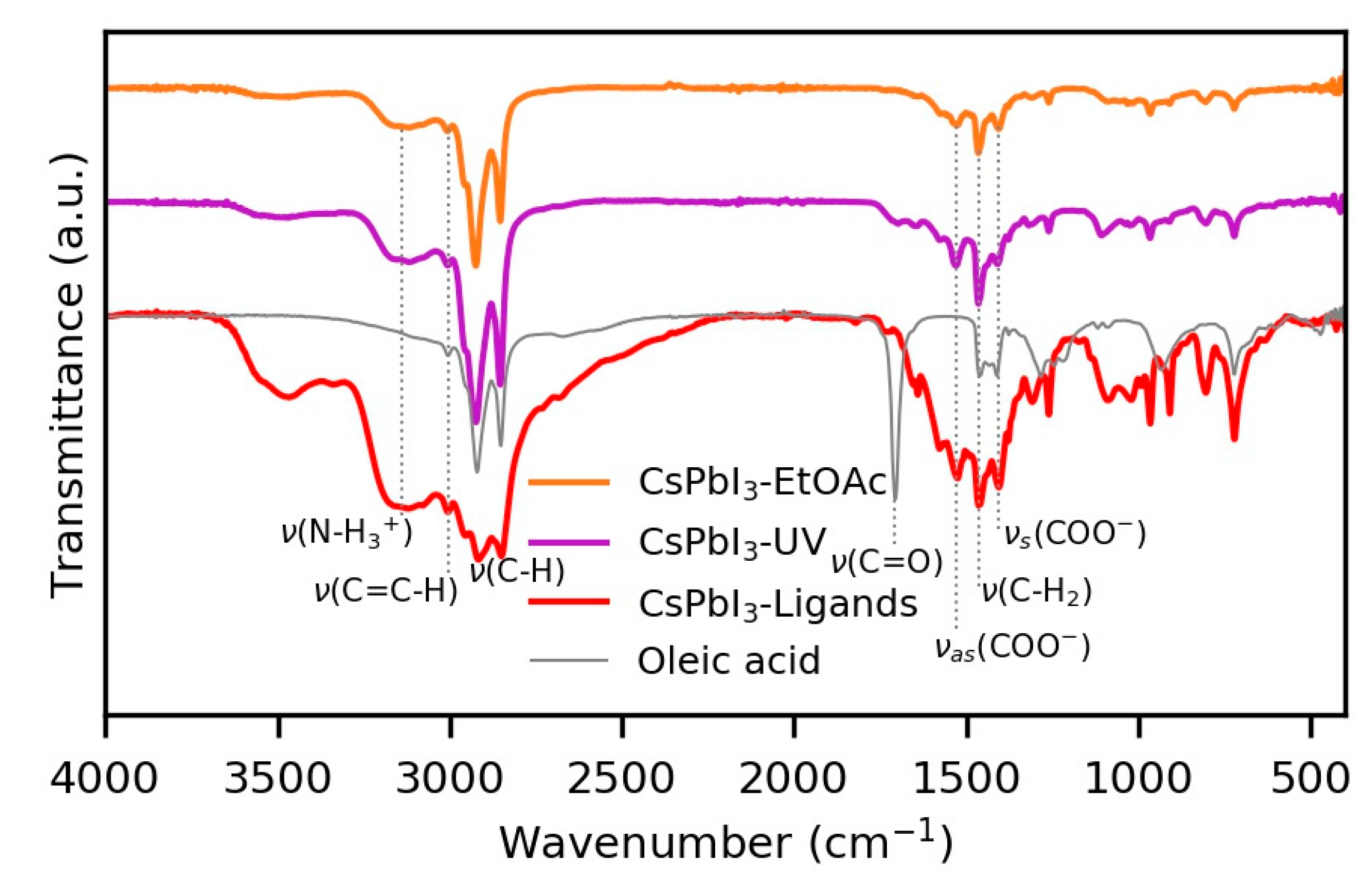
Attending to the above results, the most suitable condition is obtained for 5-layer devices, even whether the PCE is still low, so a further optimization has done only focusing on the most promising checked configurations, in terms of current densities, 3- and 5-layer devices. In order to increase the carrier transport along the perovskite QDs film, it is necessary the careful control of the ligand density covering the QDs. Oleate and oleylammonium species are removed by washing with various polar solvents. Nevertheless, excessive washing causes Cs+ vacancies and strong aggregation or degradation [16,24]. On the other hand, UV/O3 has proven to remove ligands from CsPbBr3 QDs and simultaneously increase the PL emission, by a photoactivation mechanism [25]. The QDs surface is reduced of ligands, and subsequently photo-oxidized and smoothened upon exposure to UV in air, with positive consequences, for instance, on the light emitting diodes performances [25]. Previous studies reported that no significant photo-activation is observed in a dry inert N2 atmosphere. This fact points that photo-activation is triggered mainly due to photo-oxidation [26]. Considering that the black phase of the CsPbI3 is not stable in air, we explored the use of the UV light under nitrogen atmosphere to cure the CsPbI3 QDs after the organic ligand partial removal, as a tool to improve the solar cell efficiencies, avoiding the detrimental effect of the oxygen or of the wet chemistry. A comparative analysis between the CsPbI3 films after different treatments to partially remove the organic ligand is carried out. The common washing with EtOAc and the UV treatment are used with the intention of dissolving and partial removing selectively the organic capping ligands. Figure 4 shows the FTIR spectrum of liquid neat oleic acid, with its characteristic carboxylic acid stretching mode, ν (C = O) at 1708 cm−1 [27]. This peak is not observed in the films, see Figure 4, indicating that this ligand is present as oleate species on the QDs. This is confirmed by the signals of the COO− group of the oleate [28], the symmetric and asymmetric stretching modes at 1409 and 1530 cm−1, respectively. Oleylammonium can be spotted by a broad resonance centered at 3138 cm−1 corresponding to vibrations of ammonium groups, ν (N−H3+) [14]. The peaks at ν (C−H) = 2780−3000 cm−1, ν (C = C−H) = 3005 cm−1, and ν (C−H2) = 1466 cm−1 are also related to the long alkyl chain of the oleic species or to the acetic acid formed in situ.
The signals intensity of the film washed with EtOAc are decreased, compared with the signals of the sample without washing (CsPbI3-Ligands), indicating the partial removal of organic ligands [24]. In the case of the sample subjected to UV treatment, there is no proof of substantial ligand removal induced by the UV light, as there is no significant difference in the signals intensity, thus the ligand surface density of the QDs is roughly the same. Note that with the FTIR analysis we confirm that the organic species present in solution interact with the QDs also after the UV treatment and that if the UV could be an efficient way to remove organic ligand in air under nitrogen atmosphere the FTIR shows no signs of further removal. However, the efficiency of the devices made with the UV treatment has signs to be different, which as explained below will be due to an alternative mechanism, which in this study is not ascribed to the amount of ligand coordinated with the QDs.
Figure 5 shows the statistic of the figures of merit and refers to the devices made with 3 or 5 QDs layers. In the reference devices, every spin-coated layer is washed with EtOAc to partially remove the capping ligands from the QDs surface. When the semi-devices undergoing UV treatment are put under UV radiation for 2 min after every EtOAc washing, it is found that the Jsc, the Voc, the FF, and especially the reproducibility of the devices significantly improves, see Figure 5 and Table 2. A UV exposure less than 2 min leads to the partial detachment of the layer after EtOAc washing, Figure S2.
It is also worth to note that after air exposure during J/V characterization, the solar cells without UV treatment quickly turned yellow (Figure S2b). The yellow color is due to phase transformation from black α-CsPbI3 to yellow δ-CsPbI3, as we have analyzed by X-ray diffraction (XRD), see Figure 6. By contrast, UV treated samples are stable at least during 7 days at 25% of relative humidity, see Figure 6. X-ray diffraction patterns of the CsPbI3 films confirm that fresh samples always present black α-CsPbI3 independently of the treatment. After 6 h, these films are not more stable and the peak corresponding to the yellow CsPbI3 δ-phase at 9.8° appears. However, the films treated with 2 min UV are stable at least for 7 days, as it has been previously commented. Interestingly, a too long UV treatment (4 min) cannot avoid the phase transformation into the δ-phase after 6 h [29].
On the other hand, by comparing 5-layer devices with and without UV treatment (total exposure time of 10 min), a decrease in the Jsc is observed. In line with this, the 3-layer devices exposed for 12 min to the UV (4 min for each layer) also result in a decrease in the Jsc. The Voc and FF increase even after this long exposure for both cases, but the negative effect in the current predominates and the efficiency decreases (Figure 5c,d and Table 2). Lead halide perovskites in fact suffer an aggressive degradation after prolonged UV exposure [20,30,31]. This fact indicates that the total UV exposure times longer than 10 min generate photodegradation in the perovskite, as demonstrated with the XRD measurements, Figure 6. However, reduced time UV treatments can significantly contribute to the device performance and stability. In brief, the best PCE obtained, 7.4% for the solar cells based on 3 layers treated with the UV, originated from the higher Jsc and Voc than the samples without UV, and from the higher FF than the sample with more layers, see Table 2. The incident photon-to-electron conversion efficiency (IPCE) characterization, see Figure 5f, confirms the presence of black phase of CsPbI3 in working encapsulated PQDSCs with a good agreement between the photocurrents calculated by this method and the measured by J–V curves, see Table S1, where the higher current observed in the IPCE could be due to the encapsulation of both the devices. The encapsulation was done to untangle the increased Jsc from the degradation observed in the non-treated devices, as it will be discussed later. The IPCE characterization relates also to many factors such as the band gap of the photoactive material [32,33,34], the light that goes through the transparent electrodes and the effectiveness of charge collection at certain wavelength [32,35]. The shape of the IPCE spectra is consistent with previous work, reporting direct planar solar cells architecture, where the onset at short wavelengths is related to light absorbance from the ITO glass and SnO2 [18] and the one at the long wavelengths is at 680 nm, below the onset around 700 nm of solar cells employing bulk CsPbI3. This demonstrates the preservation of the quantum confinement for both non-treated and UV treated devices [4,15,36,37].
The optical properties are analyzed in Figure 7. The absorption spectra, see Figure 7a, of the untreated film confirms, in accordance with the XRD (Figure 6), the fast degradation of the sample without UV treatment, as the peak around 416 nm evidences the presence of CsPbI3 yellow phase (δ-CsPbI3) [38]. Moreover, there is no change in the absorbance intensity at the onset, so the UV does not affect the layer thickness. The photoluminescence (PL) spectra show a blue shift from 680 to 675 and an increase in the full width half maximum (FWHM) from 51 nm to 57 nm (Figure 7 b) in line with the underway degradation of the CsPbI3-EtOAc. In addition, it has been found that after the UV treatment, QDs have longer PL time decay with electron lifetime, see Figure 7c, going from 1.9 ns to 11.8 ns, Table S2, representative of the surface emission trap concentration reduction [39]. This behavior can be attributed to either long carrier diffusion length in bigger CsPbI3 domains, as in the case of CsPbBr3 [20], or to the passivation of the defects and a lower non-radiative recombination processes. The enlargement of the QDs size is not corroborated, as the PL emission of the CsPbI3-UV is at the same wavelength of the original CsPbI3, see Figure 1. Thus, the only mechanism plausible to explain the longer time decay remains the decrease of the non-radiative recombination. Accordingly, despite the same thickness of the layers with and without UV treatment, the Jsc of the devices based on the material treated with UV is higher. The slow and constant degradation of the samples without UV also can contribute to a lower current value, but the preservation of the bandgap observed in the IPCE for encapsulated device clearly demonstrated that the degradation process is not the main cause of the lower Jsc. Instead, the reduction of the non-radiative recombination is correlated with the improved solar cells.
Finally, the most notable difference of the short duration UV treatment is the improved ambient stability of the QDs films. We propose a mechanism to understand this behavior, summarized in Scheme 1. It is well known that the surface vacancies would generate substantial dangling bonds absorbing moisture that accelerate the phase transition [36]. Since the surface vacancies in the QDs with and without UV treatment are not determined by difference in the chemical surrounding, as we have demonstrated by FTIR and since inside the glovebox photo-oxidation unlikely occurs, the rise of the observed improved stability is explained through another mechanism. It has been demonstrated that the α- and δ-phases internal energy difference decreases upon creation of cation vacancies defects [40]. They have a higher formation energies in δ-phase [40] while in the α-phase, the organic ligands coordinate the cations and create Cs-oleate and Pb-oleate pairs, by extracting metal cations from the surface and leave cation vacancies, according to the nanosizing effect [16,40]. These vacancies diffuse into the QDs bulk due to the short migration path that requires the passage of metal cations from the center of the QDs to the surface, passivating superficial vacancies and reducing the surface recombination centers, see Scheme 1 [40]. Following the postulated above, a possible explanation for the increased stability is as follows. Cs+ vacancies are created by EtOAc washing that carries some of the bound ligands (Cs-oleate) off the surface. Vacancies created are, in theory, detrimental to the stability of QDs, as is the case of the UV-free films. In the case of UV treatment, the increased ion mobility in perovskite materials [22,41,42,43] facilitates the migration of cations from the interior of the QDs to the surface (Scheme 1), in line with the mechanism postulated by Y. Kye et al. for which the presence of cation vacancies in the QD bulk stabilizes α-CsPbI3 [40].
4. Conclusions
In conclusion, a time limited UV treatment is successfully used to improve the stability of the CsPbI3 QDs. The untreated material shows signs of degradation both during the spin-coating of the layer on top and always in air and in turn the untreated device degrades after exposure to air, as demonstrated by the presence of photoinactive δ-CsPbI3. The improved current and PCE for the device with the short UV treatment is related with a more air stable material, facile and robust interface optimization, and decreased non-radiative recombination. Finally, a material stable for 200 h and devices with a higher reproducible efficiency of the 7.4% have been obtained, demonstrating that the control of cation vacancies without using the wet chemistry is a promising route for the improvement of the perovskite QDs solar cells.
Supplementary Materials
The following are available online at https://0-www-mdpi-com.brum.beds.ac.uk/2079-4991/10/8/1586/s1, Figure S1: Top view SEM image of the CsPbI3 QDs 3 layer film with higher magnification, Figure S2: (a) Photograph of accidental detachment of photoactive layer after EtOAc washing in a device with 1 min UV treatment. (b) Pictures of the solar cells after air exposure, left EtOAc and right UV treated device, Table S1: Photovoltaic parameters extracted from J–Vs scans, best device of each variation, Table S2: Time resolved PL decay fitting parameters with a biexponential function.
Author Contributions
Data curation, E.A.E., H.E.S.-G., A.F.G.-R., and S.M.; formal analysis, S.M. and I.M.-S.; funding acquisition, I.M.-S.; resources, I.M.-S.; supervision, S.M. and I.M.-S.; writing—original draft, E.A.E., S.M., and I.M.-S. All authors have read and agreed to the published version of the manuscript.
Funding
Financial support from the European Research Council (ERC) via Consolidator Grant (724424-No-LIMIT) and Generalitat Valenciana via Prometeo Grant Q-Devices (Prometeo/2018/098) is gratefully acknowledged. Eider A. Erazo also acknowledges support from Facultad de Ciencias Universidad de los Andes (Proyecto INV-2019-86-1798) and CEIBA foundation. H.E Sanchez-Godoy acknowledges to CONACYT for the financial support to a short stay at INAM.
Acknowledgments
We thank SCIC of University Jaume I for its help with TEM, FTIR, XRD and SEM measurements.
Conflicts of Interest
The authors declare no conflict of interest.
References
- NREL Best Research-Cell Efficiencies. Available online: https://www.nrel.gov/pv/assets/pdfs/best-research-cell-efficiencies.20200406.pdf (accessed on 10 July 2020).
- Masi, S.; Gualdrón-Reyes, A.F.; Mora-Seró, I. Stabilization of Black Perovskite Phase in FAPbI3 and CsPbI3. ACS Energy Lett. 2020, 1974–1985. [Google Scholar] [CrossRef]
- Becker, M.; Klüner, T.; Wark, M. Formation of hybrid ABX3 perovskite compounds for solar cell application: First-principles calculations of effective ionic radii and determination of tolerance factors. Dalt. Trans. 2017, 46, 3500–3509. [Google Scholar] [CrossRef] [PubMed]
- Swarnkar, A.; Marshall, A.R.; Sanehira, E.M.; Chernomordik, B.D.; Moore, D.T.; Christians, J.A.; Chakrabarti, T.; Luther, J.M. Quantum dot-induced phase stabilization of -CsPbI3 perovskite for high-efficiency photovoltaics. Science 2016, 354, 92–95. [Google Scholar] [CrossRef] [PubMed] [Green Version]
- Chen, K.; Jin, W.; Zhang, Y.; Yang, T.; Reiss, P.; Zhong, Q.; Bach, U.; Li, Q.; Wang, Y.; Zhang, H.; et al. High Efficiency Mesoscopic Solar Cells Using CsPbI3 Perovskite Quantum Dots Enabled by Chemical Interface Engineering. J. Am. Chem. Soc. 2020, 142, 3775–3783. [Google Scholar] [CrossRef] [Green Version]
- Hao, M.; Bai, Y.; Zeiske, S.; Ren, L.; Liu, J.; Yuan, Y.; Zarrabi, N.; Cheng, N.; Ghasemi, M.; Chen, P.; et al. Ligand-assisted cation-exchange engineering for high-efficiency colloidal Cs1−xFAxPbI3 quantum dot solar cells with reduced phase segregation. Nat. Energy 2020, 5, 79–88. [Google Scholar] [CrossRef]
- Sanehira, E.M.; Marshall, A.R.; Christians, J.A.; Harvey, S.P.; Ciesielski, P.N.; Wheeler, L.M.; Schulz, P.; Lin, L.Y.; Beard, M.C.; Luther, J.M. Enhanced mobility CsPbI3 quantum dot arrays for record-efficiency, high-voltage photovoltaic cells. Sci. Adv. 2017, 3, eaao4204. [Google Scholar] [CrossRef] [Green Version]
- Yuan, J.; Ling, X.; Yang, D.; Li, F.; Zhou, S.; Shi, J.; Qian, Y.; Hu, J.; Sun, Y.; Yang, Y.; et al. Band-Aligned Polymeric Hole Transport Materials for Extremely Low Energy Loss α-CsPbI3 Perovskite Nanocrystal Solar Cells. Joule 2018, 2, 2450–2463. [Google Scholar] [CrossRef] [Green Version]
- Draguta, S.; Sharia, O.; Yoon, S.J.; Brennan, M.C.; Morozov, Y.V.; Manser, J.S.; Kamat, P.V.; Schneider, W.F.; Kuno, M. Rationalizing the light-induced phase separation of mixed halide organic–inorganic perovskites. Nat. Commun. 2017, 8, 200. [Google Scholar] [CrossRef] [Green Version]
- Gualdrón-Reyes, A.F.; Yoon, S.J.; Mora-Seró, I. Recent insights for achieving mixed halide perovskites without halide segregation. Curr. Opin. Electrochem. 2018, 11, 84–90. [Google Scholar] [CrossRef]
- Gualdrón-Reyes, A.F.; Yoon, S.J.; Barea, E.M.; Agouram, S.; Muñoz-Sanjosé, V.; Meléndez, Á.M.; Niño-Gómez, M.E.; Mora-Seró, I. Controlling the Phase Segregation in Mixed Halide Perovskites through Nanocrystal Size. ACS Energy Lett. 2019, 4, 54–62. [Google Scholar] [CrossRef]
- Yuan, J.; Hazarika, A.; Zhao, Q.; Ling, X.; Moot, T.; Ma, W.; Luther, J.M. Metal Halide Perovskites in Quantum Dot Solar Cells: Progress and Prospects. Joule 2020, 4, 1160–1185. [Google Scholar] [CrossRef]
- Zhao, Q.; Hazarika, A.; Chen, X.; Harvey, S.P.; Larson, B.W.; Teeter, G.R.; Liu, J.; Song, T.; Xiao, C.; Shaw, L.; et al. High efficiency perovskite quantum dot solar cells with charge separating heterostructure. Nat. Commun. 2019, 10, 2842. [Google Scholar] [CrossRef]
- Wheeler, L.M.; Sanehira, E.M.; Marshall, A.R.; Schulz, P.; Suri, M.; Anderson, N.C.; Christians, J.A.; Nordlund, D.; Sokaras, D.; Kroll, T.; et al. Targeted Ligand-Exchange Chemistry on Cesium Lead Halide Perovskite Quantum Dots for High-Efficiency Photovoltaics. J. Am. Chem. Soc. 2018, 140, 10504–10513. [Google Scholar] [CrossRef]
- Fu, Y.; Rea, M.T.; Chen, J.; Morrow, D.J.; Hautzinger, M.P.; Zhao, Y.; Pan, D.; Manger, L.H.; Wright, J.C.; Goldsmith, R.H.; et al. Selective Stabilization and Photophysical Properties of Metastable Perovskite Polymorphs of CsPbI3 in Thin Films. Chem. Mater. 2017, 29, 8385–8394. [Google Scholar] [CrossRef]
- Ling, X.; Zhou, S.; Yuan, J.; Shi, J.; Qian, Y.; Larson, B.W.; Zhao, Q.; Qin, C.; Li, F.; Shi, G.; et al. 14.1% CsPbI3 Perovskite Quantum Dot Solar Cells via Cesium Cation Passivation. Adv. Energy Mater. 2019, 9, 1900721. [Google Scholar] [CrossRef]
- Chen, K.; Zhong, Q.; Chen, W.; Sang, B.; Wang, Y.; Yang, T.; Liu, Y.; Zhang, Y.; Zhang, H. Short-Chain Ligand-Passivated Stable α-CsPbI3 Quantum Dot for All-Inorganic Perovskite Solar Cells. Adv. Funct. Mater. 2019, 29, 1900991. [Google Scholar] [CrossRef]
- Jia, D.; Chen, J.; Yu, M.; Liu, J.; Johansson, E.M.J.; Hagfeldt, A.; Zhang, X. Dual Passivation of CsPbI3 Perovskite Nanocrystals with Amino Acid Ligands for Efficient Quantum Dot Solar Cells. Small 2020, 16, 2001772. [Google Scholar] [CrossRef]
- Pan, L.; Ye, T.; Qin, C.; Zhou, B.; Lei, N.; Chen, S.; Yan, P.; Wang, X. α-CsPbI3 Nanocrystals by Ultraviolet Light-Driven Oriented Attachment. J. Phys. Chem. Lett. 2020, 11, 913–919. [Google Scholar] [CrossRef]
- Liu, J.; Song, K.; Shin, Y.; Liu, X.; Chen, J.; Yao, K.X.; Pan, J.; Yang, C.; Yin, J.; Xu, L.-J.; et al. Light-Induced Self-Assembly of Cubic CsPbBr3 Perovskite Nanocrystals into Nanowires. Chem. Mater. 2019, 31, 6642–6649. [Google Scholar] [CrossRef]
- Thapa, S.; Bhardwaj, K.; Basel, S.; Pradhan, S.; Eling, C.J.; Adawi, A.M.; Bouillard, J.S.G.; Stasiuk, G.J.; Reiss, P.; Pariyar, A.; et al. Long-term ambient air-stable cubic CsPbBr3 perovskite quantum dots using molecular bromine. Nanoscale Adv. 2019, 1, 3388–3391. [Google Scholar] [CrossRef] [Green Version]
- Wang, Y.; Li, X.; Sreejith, S.; Cao, F.; Wang, Z.; Stuparu, M.C.; Zeng, H.; Sun, H. Photon Driven Transformation of Cesium Lead Halide Perovskites from Few-Monolayer Nanoplatelets to Bulk Phase. Adv. Mater. 2016, 28, 10637–10643. [Google Scholar] [CrossRef] [PubMed]
- Méndez, P.F.; Muhammed, S.K.M.; Barea, E.M.; Masi, S.; Mora-Seró, I. Analysis of the UV-Ozone-Treated SnO2 Electron Transporting Layer in Planar Perovskite Solar Cells for High Performance and Reduced Hysteresis. Sol. RRL 2019, 3, 1900191. [Google Scholar] [CrossRef]
- Liu, F.; Zhang, Y.; Ding, C.; Kobayashi, S.; Izuishi, T.; Nakazawa, N.; Toyoda, T.; Ohta, T.; Hayase, S.; Minemoto, T.; et al. Highly Luminescent Phase-Stable CsPbI3 Perovskite Quantum Dots Achieving Near 100% Absolute Photoluminescence Quantum Yield. ACS Nano 2017, 11, 10373–10383. [Google Scholar] [CrossRef] [PubMed]
- Moyen, E.; Kanwat, A.; Cho, S.; Jun, H.; Aad, R.; Jang, J. Ligand removal and photo-activation of CsPbBr3 quantum dots for enhanced optoelectronic devices. Nanoscale 2018, 10, 8591–8599. [Google Scholar] [CrossRef]
- Carrillo-Carrión, C.; Cárdenas, S.; Simonet, B.M.; Valcárcel, M. Quantum dots luminescence enhancement due to illumination with UV/V is light. Chem. Commun. 2009, 35, 5214. [Google Scholar] [CrossRef]
- Shi, Y.Y.; Sun, B.; Zhou, Z.; Wu, Y.T.; Zhu, M.F. Size-controlled and large-scale synthesis of organic-soluble Ag nanocrystals in water and their formation mechanism. Prog. Nat. Sci. Mater. Int. 2011, 21, 447–454. [Google Scholar] [CrossRef] [Green Version]
- Hassanabadi, E.; Latifi, M.; Gualdrón-Reyes, A.F.; Masi, S.; Yoon, S.J.; Poyatos, M.; Julián-López, B.; Mora-Seró, I. Ligand & band gap engineering: Tailoring the protocol synthesis for achieving high-quality CsPbI3 quantum dots. Nanoscale 2020. [Google Scholar] [CrossRef]
- Zhang, T.; Dar, M.I.; Li, G.; Xu, F.; Guo, N.; Grätzel, M.; Zhao, Y. Bication lead iodide 2D perovskite component to stabilize inorganic α-CsPbI3 perovskite phase for high-efficiency solar cells. Sci. Adv. 2017, 3, e1700841. [Google Scholar] [CrossRef] [Green Version]
- Quitsch, W.A.; Dequilettes, D.W.; Pfingsten, O.; Schmitz, A.; Ognjanovic, S.; Jariwala, S.; Koch, S.; Winterer, M.; Ginger, D.S.; Bacher, G. The Role of Excitation Energy in Photobrightening and Photodegradation of Halide Perovskite Thin Films. J. Phys. Chem. Lett. 2018, 9, 2062–2069. [Google Scholar] [CrossRef]
- Li, Q.; Ji, S.; Yuan, X.; Li, J.; Fan, Y.; Zhang, J.; Zhao, J.; Li, H. Ultraviolet Light-Induced Degradation of Luminescence in Mn-Doped CsPbCl3 Nanocrystals. J. Phys. Chem. C 2019, 123, 14849–14857. [Google Scholar] [CrossRef]
- Tai, Q.; Tang, K.-C.; Yan, F. Recent progress of inorganic perovskite solar cells. Energy Environ. Sci. 2019, 12, 2375–2405. [Google Scholar] [CrossRef]
- Kulkarni, S.A.; Baikie, T.; Boix, P.P.; Yantara, N.; Mathews, N.; Mhaisalkar, S. Band-gap tuning of lead halide perovskites using a sequential deposition process. J. Mater. Chem. A 2014, 2, 9221–9225. [Google Scholar] [CrossRef] [Green Version]
- Shen, T.; Tian, J.; Lv, L.; Fei, C.; Wang, Y.; Pullerits, T.; Cao, G. Investigation of the role of Mn dopant in CdS quantum dot sensitized solar cell. Electrochim. Acta 2016, 191, 62–69. [Google Scholar] [CrossRef]
- Nakane, A.; Tampo, H.; Tamakoshi, M.; Fujimoto, S.; Kim, K.M.; Kim, S.; Shibata, H.; Niki, S.; Fujiwara, H. Quantitative determination of optical and recombination losses in thin-film photovoltaic devices based on external quantum efficiency analysis. J. Appl. Phys. 2016, 120, 064505. [Google Scholar] [CrossRef]
- Ding, X.; Cai, M.; Liu, X.; Ding, Y.; Liu, X.; Wu, Y.; Hayat, T.; Alsaedi, A.; Dai, S. Enhancing the Phase Stability of Inorganic α-CsPbI3 by the Bication-Conjugated Organic Molecule for Efficient Perovskite Solar Cells. ACS Appl. Mater. Interfaces 2019, 11, 37720–37725. [Google Scholar] [CrossRef] [PubMed]
- Duan, J.; Xu, H.; Sha, W.E.I.; Zhao, Y.; Wang, Y.; Yang, X.; Tang, Q. Inorganic perovskite solar cells: An emerging member of the photovoltaic community. J. Mater. Chem. A 2019, 7, 21036–21068. [Google Scholar] [CrossRef]
- Shi, J.; Wang, Y.; Zhao, Y. Inorganic CsPbI3 Perovskites toward High-Efficiency Photovoltaics. Energy Environ. Mater. 2019, 2, 73–78. [Google Scholar] [CrossRef] [Green Version]
- Wang, H.; Zhang, X.; Sui, N.; Hu, Y.; Colvin, V.L.; Yu, W.W.; Zhang, Y. Photoluminescence Loss and Recovery of α-CsPbI3 Quantum Dots Originated from Chemical Equilibrium Shift of Oleylammonium. ACS Appl. Mater. Interfaces 2020, 12, 11769–11777. [Google Scholar] [CrossRef]
- Kye, Y.-H.; Yu, C.-J.; Jong, U.-G.; Ri, K.-C.; Kim, J.-S.; Choe, S.-H.; Hong, S.-N.; Li, S.; Wilson, J.N.; Walsh, A. Vacancy-Driven Stabilization of the Cubic Perovskite Polymorph of CsPbI3. J. Phys. Chem. C 2019, 123, 9735–9744. [Google Scholar] [CrossRef] [Green Version]
- Domanski, K.; Roose, B.; Matsui, T.; Saliba, M.; Turren-Cruz, S.H.; Correa-Baena, J.P.; Carmona, C.R.; Richardson, G.; Foster, J.M.; De Angelis, F.; et al. Migration of cations induces reversible performance losses over day/night cycling in perovskite solar cells. Energy Environ. Sci. 2017, 10, 604–613. [Google Scholar] [CrossRef] [Green Version]
- Ghosh, S.; Shi, Q.; Pradhan, B.; Mushtaq, A.; Acharya, S.; Karki, K.J.; Pullerits, T.; Pal, S.K. Light-Induced Defect Healing and Strong Many-Body Interactions in Formamidinium Lead Bromide Perovskite Nanocrystals. J. Phys. Chem. Lett. 2020, 11, 1239–1246. [Google Scholar] [CrossRef] [PubMed]
- Wei, Y.; Cheng, Z.; Lin, J. An overview on enhancing the stability of lead halide perovskite quantum dots and their applications in phosphor-converted LEDs. Chem. Soc. Rev. 2019, 48, 310–350. [Google Scholar] [CrossRef] [PubMed]
Figure 1.
(A) TEM image of the CsPbI3 quantum dots (QDs) synthetized at 170 °C (inset: CsPbI3 QDs solution in octane), (B) CsPbI3 QDs size distribution histogram, (C) absorption and emission spectra of the synthetized CsPbI3 QDs in solution.
Figure 1.
(A) TEM image of the CsPbI3 quantum dots (QDs) synthetized at 170 °C (inset: CsPbI3 QDs solution in octane), (B) CsPbI3 QDs size distribution histogram, (C) absorption and emission spectra of the synthetized CsPbI3 QDs in solution.

Figure 2.
(A) Sketch of the perovskite solar cells architecture; photovoltaic statistic (box plot) of the QDs solar cells figures of merit, with different number of layers stacked by spin-coating and ethyl-acetate (EtOAc) washings: (B) power conversion efficiency PCE. (C) Short circuit current density, Jsc. (D) Open circuit voltage, Voc. (E) Fill factor, FF.

Figure 3.
Top view SEM images of the CsPbI3 QDs films deposited layer by layer. (A) 3 layers, (B) 5 layers, (C) 7 layers. Cross section SEM images of the staked CsPbI3 QDs layers deposited over the SnO2 electron transporting layer (ETL). (D) 3 layers, (E) 5 layers, and (F) 7 layers.
Figure 3.
Top view SEM images of the CsPbI3 QDs films deposited layer by layer. (A) 3 layers, (B) 5 layers, (C) 7 layers. Cross section SEM images of the staked CsPbI3 QDs layers deposited over the SnO2 electron transporting layer (ETL). (D) 3 layers, (E) 5 layers, and (F) 7 layers.

Figure 4.
FTIR spectra of neat oleic acid (gray) and spin-coated CsPbI3 QDs film (without EtOAc washing of the film): CsPbI3 Ligands (red); spin-coated film washed with EtOAc: CsPbI3-EtOAc (orange). Spin-coated layer exposed to UV light for 2 min after washing: CsPbI3-UV (purple). In all the cases the film constituted of 1 spin-coated layer of QDs.

Figure 5.
Photovoltaic parameters of the CsPbI3 perovskite QDs solar cells with different number of layers and UV treatments. EtOAc is the sample in which only the EtOAc washing is used. UV means that each layer was treated with the UV under nitrogen after every washing. Box plots for (A) power conversion efficiency, PCE. (B) Short circuit current density, Jsc. (C) Open circuit voltage, Voc. (D) Fill factor, FF. (E) J–V curves of the best solar cells employing 3 layers of CsPbI3 QDs stacked by washing (EtOAc) and washing + UV treatment. (F) IPCE curves of encapsulated solar cells with 3 layers of CsPbI3 QDs as light absorber with and without UV treatment.

Figure 6.
XRD patterns of the CsPbI3-ligand (1 layer), CsPbI3-EtOAc (3 layers), and UV treated (3 layers) fresh samples and after 7 days in air; different UV exposure times (2 min and 4 min) are reported.
Figure 6.
XRD patterns of the CsPbI3-ligand (1 layer), CsPbI3-EtOAc (3 layers), and UV treated (3 layers) fresh samples and after 7 days in air; different UV exposure times (2 min and 4 min) are reported.

Figure 7.
Optical characterization of CsPbI3 QDs 3 stacked layers deposited on glass with and without UV treatment. (A) Normalized absorption spectra, (B) steady state PL emission spectra, excitation wavelength 530 nm, and (C) time resolved PL decay fitted whit a biexponential decay function.
Figure 7.
Optical characterization of CsPbI3 QDs 3 stacked layers deposited on glass with and without UV treatment. (A) Normalized absorption spectra, (B) steady state PL emission spectra, excitation wavelength 530 nm, and (C) time resolved PL decay fitted whit a biexponential decay function.

Scheme 1.
Sketch of the photo induced phase stabilization of CsPbI3 QDs: At first, surface cation vacancies are created during de EtOAc washing by the removal of Cs-oleate. Surface cation vacancies are detrimental for the phase stability. The UV exposure enhances ionic mobility and the cation vacancies diffuse to the QD bulk stabilizing the cubic phase.


Table 1.
Mean and standard deviation (SD) for the photovoltaic figures of merit of devices with different number of QDs layers.
Table 1.
Mean and standard deviation (SD) for the photovoltaic figures of merit of devices with different number of QDs layers.
| Number of Layers | PCE (%) (Mean ± SD) | Jsc (mA/cm2) (Mean ± SD) | Voc (V) (Mean ± SD) | FF (%) (Mean ± SD) |
|---|---|---|---|---|
| 3 | 3.7 ± 1.8 | 8.4 ± 1.3 | 0.840 ± 0.290 | 47.4 ± 16.2 |
| 5 | 4.2 ± 1.9 | 7.9 ± 2.0 | 0.921 ± 0.192 | 53.9 ± 14.7 |
| 7 | 3.0 ± 1.7 | 7.0 ± 0.8 | 0.776 ± 0.270 | 47.9 ± 15.1 |
| 10 | 2.8 ± 1.4 | 6.7 ± 1.6 | 0.810 ± 0.220 | 46.0 ± 12.8 |
Table 2.
Mean and standard deviation (SD) for the photovoltaic figures of merit of devices with different number of QDs layers.
Table 2.
Mean and standard deviation (SD) for the photovoltaic figures of merit of devices with different number of QDs layers.
| Variation | PCE (%) (Mean ± SD) | Jsc (mA/cm2) (Mean ± SD) | Voc (V) (Mean ± SD) | FF (%) (Mean ± SD) | Best PCE (%) |
|---|---|---|---|---|---|
| EtOAc 3 L | 3.7 ± 1.8 | 8.4 ± 1.3 | 0.840 ± 0.290 | 47.4 ± 16.2 | 5.8 |
| EtOAc 5 L | 4.2 ± 1.9 | 7.9 ± 2.0 | 0.921 ± 0.192 | 53.9 ± 14.7 | 6.2 |
| UV 2 min 3 L | 6.7 ± 0.4 | 9.8 ± 0.4 | 1.025 ± 0.047 | 66.6 ± 3.5 | 7.4 |
| UV 2 min 5 L | 3.9 ± 1.2 | 6.8 ± 1.4 | 0.961 ± 0.066 | 57.7 ± 6.5 | 5.2 |
| UV 4 min 3 L | 3.4 ± 1.3 | 6.9 ± 1.0 | 0.864 ± 0.145 | 55.4 ± 12.7 | 5.7 |
© 2020 by the authors. Licensee MDPI, Basel, Switzerland. This article is an open access article distributed under the terms and conditions of the Creative Commons Attribution (CC BY) license (http://creativecommons.org/licenses/by/4.0/).
Share and Cite
MDPI and ACS Style
Erazo, E.A.; Sánchez-Godoy, H.E.; Gualdrón-Reyes, A.F.; Masi, S.; Mora-Seró, I. Photo-Induced Black Phase Stabilization of CsPbI3 QDs Films. Nanomaterials 2020, 10, 1586. https://0-doi-org.brum.beds.ac.uk/10.3390/nano10081586
AMA Style
Erazo EA, Sánchez-Godoy HE, Gualdrón-Reyes AF, Masi S, Mora-Seró I. Photo-Induced Black Phase Stabilization of CsPbI3 QDs Films. Nanomaterials. 2020; 10(8):1586. https://0-doi-org.brum.beds.ac.uk/10.3390/nano10081586
Chicago/Turabian StyleErazo, Eider A., H.E. Sánchez-Godoy, Andrés F. Gualdrón-Reyes, Sofia Masi, and Iván Mora-Seró. 2020. "Photo-Induced Black Phase Stabilization of CsPbI3 QDs Films" Nanomaterials 10, no. 8: 1586. https://0-doi-org.brum.beds.ac.uk/10.3390/nano10081586
Note that from the first issue of 2016, this journal uses article numbers instead of page numbers. See further details here.