
Obtaining Nanostructured ZnO onto Si Coatings for Optoelectronic Applications via Eco-Friendly Chemical Preparation Routes

 ,
,  , , ,
, , ,
Abstract
:
1. Introduction
2. Materials and Methods
2.1. Materials
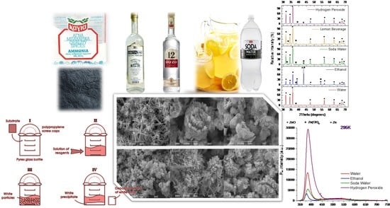
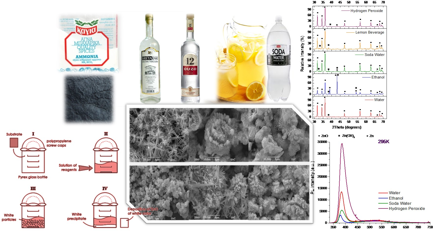
2.2. Syntheses
- The amount of 50 mL of equimolar (0.01 M) aqueous solution of Zn(NO3)2·6H2O and HMTA was placed in a common laboratory oven preheated at a specific temperature (95 °C or 195 °C) for 2 h, followed by washing with deionized water to remove residual contaminants.
- The amount of 50 mL of equimolar (0.01 M) aqueous solution of Zn(CH3COO)2·2H2O and HMTA was placed in a common laboratory oven preheated at a specific temperature (95 °C or 195 °C) for 2 h, followed by washing with deionized water to remove residual contaminants.
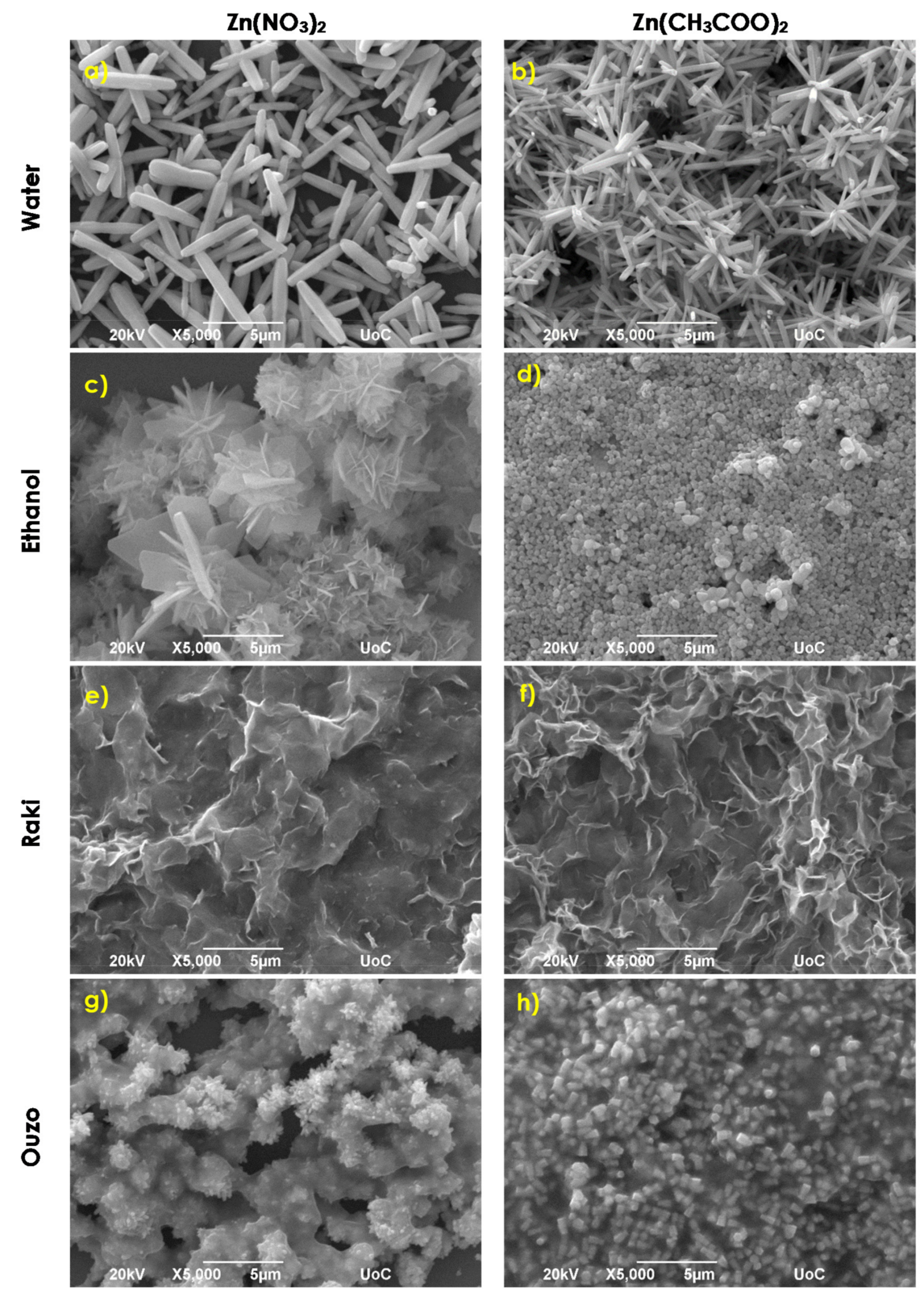
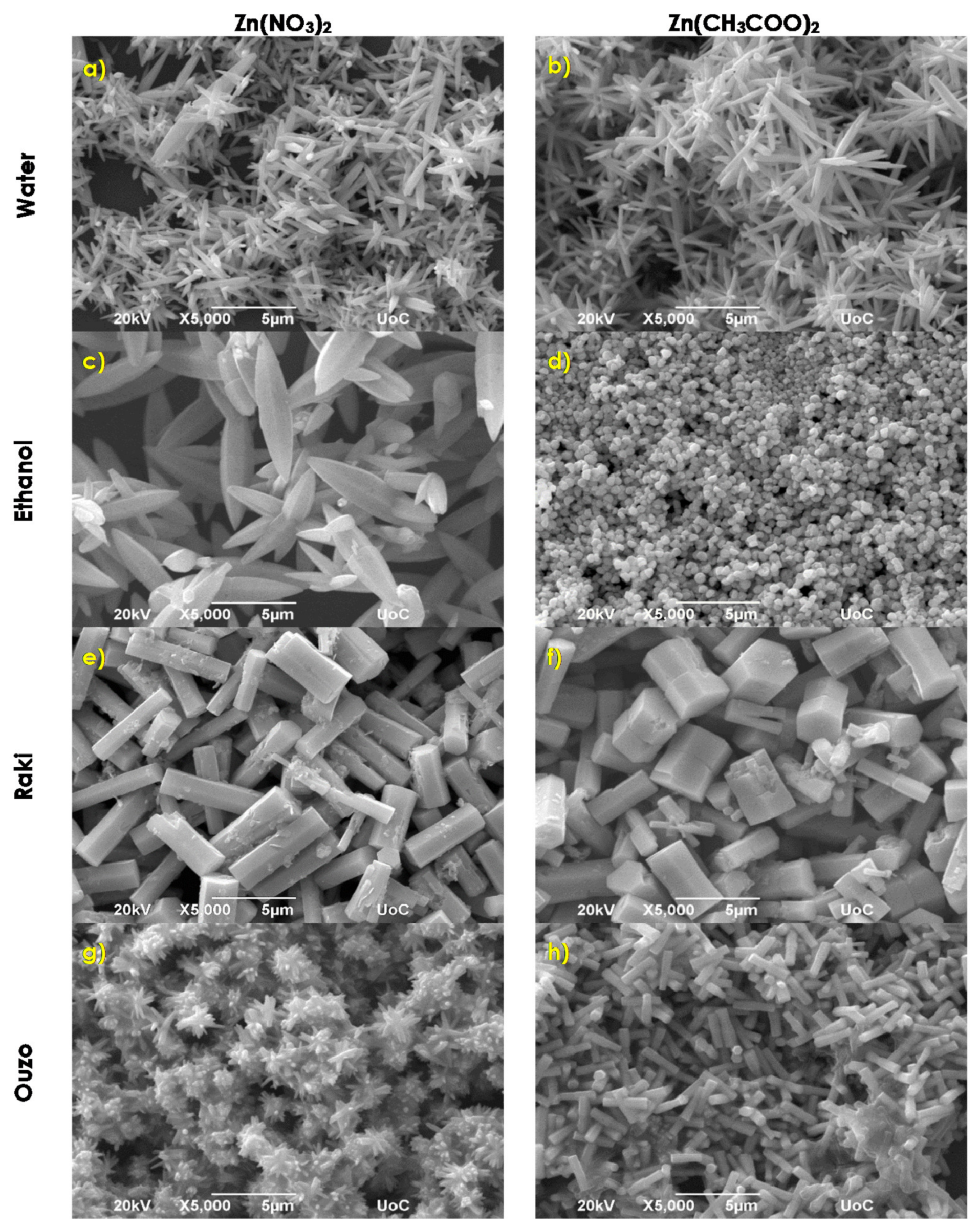
- Replacing the water with ethanol, raki, and Ouzo for 1 and 2 synthesis conditions.
- Replacing HMTA with the nontoxic baking ammonia for 1, 2, and 3 synthesis conditions.
- Replacing the Zn source with Zn metallic. The amount of 1.8 g metallic Zn powder was dissolved in 35 mL of distilled water and 0.05 g HMTA under continuous stirring, followed by thermal treatment in a laboratory oven at 195 °C for 24 h. Washing occurred after.
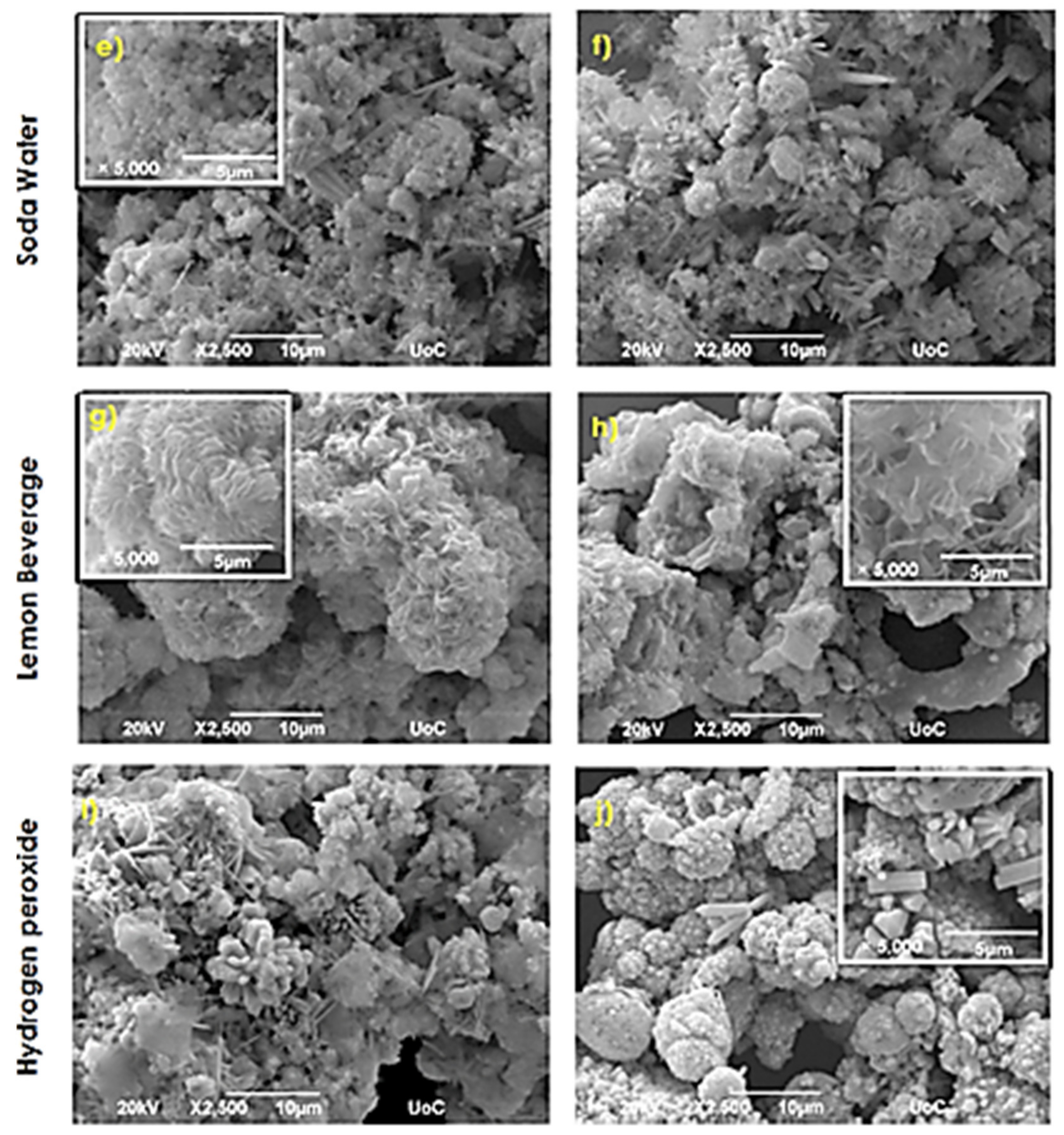
- Replacing water in synthesis 5 conditions with ethanol, soda water, lemon soft drink, and hydrogen peroxide (2.8% w/w).
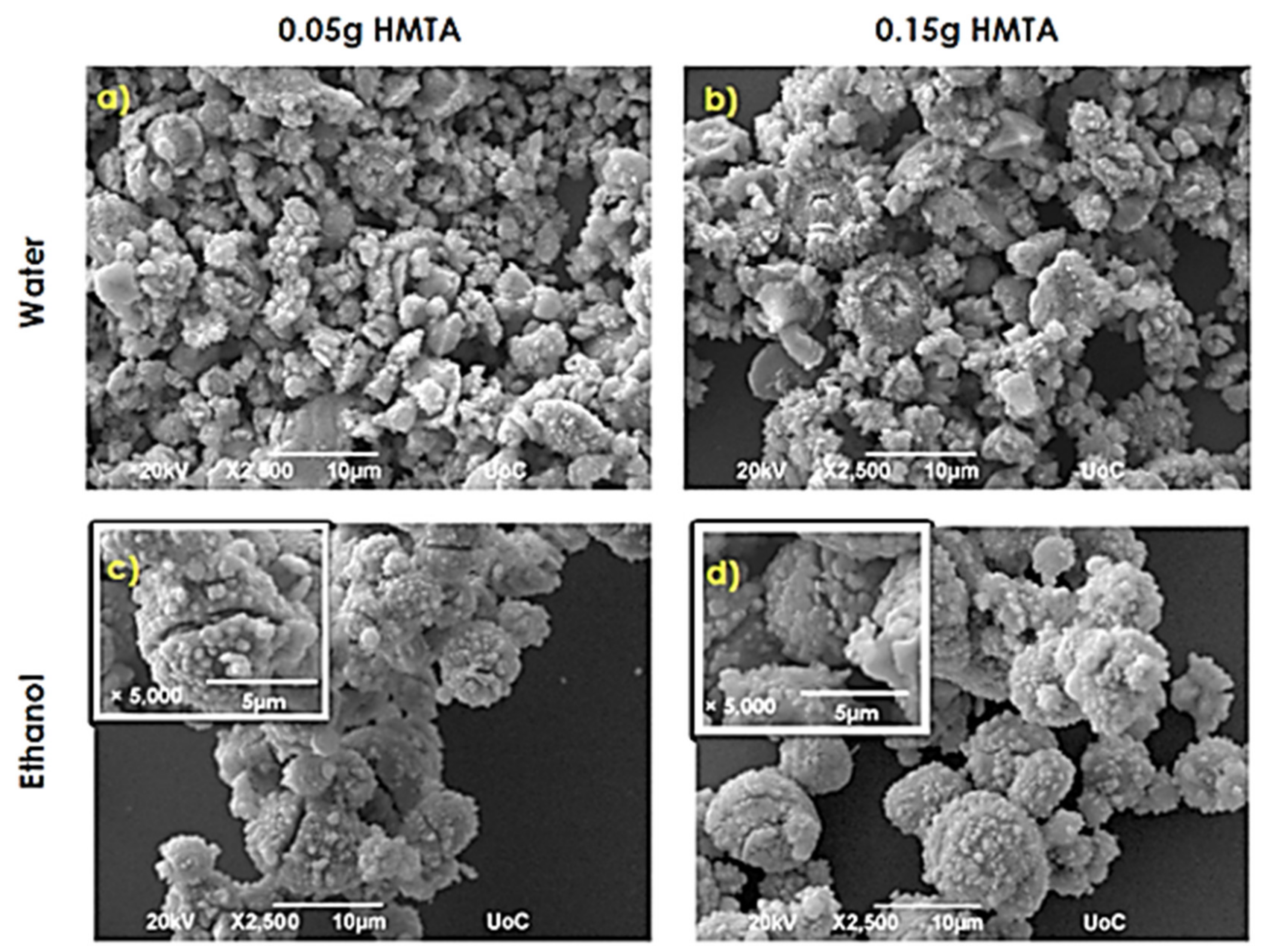
- Changing the HMTA amount. Experiments that use 0.15 g instead of 0.05 g HMTA were also performed under the exact same procedure by using the different solvents (water, soda water, lemon soft drink, and hydrogen peroxide).
- Replacing the HMTA with 0.05 g and 0.15 g nontoxic baking ammonia in synthesis 5 and 6 conditions.
- Elimination of the amine: 1.8 g metallic Zn powder dissolved in 35 mL of the desired solvent (distilled water, ethanol, soda water, and hydrogen peroxide), followed by thermal treatment in a laboratory oven at 195 °C for 24 h. Washing occurred after.
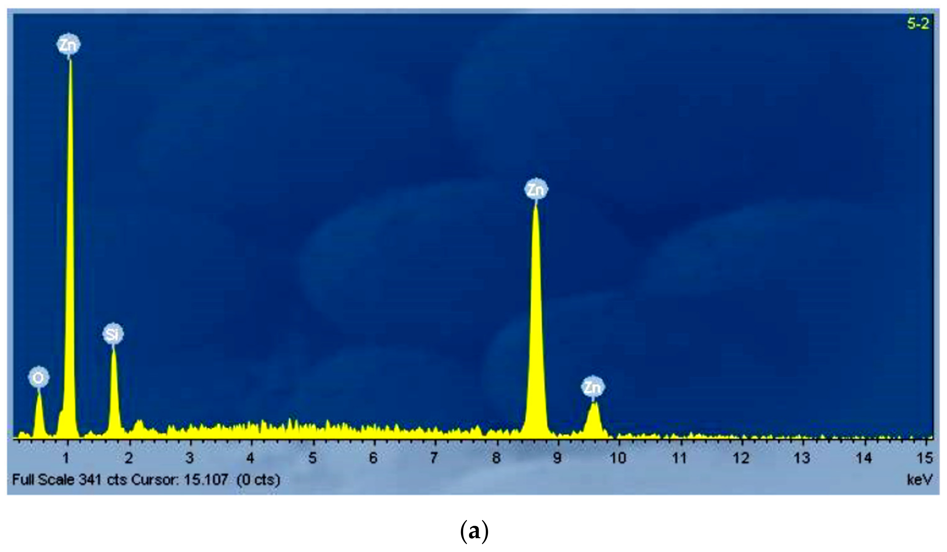
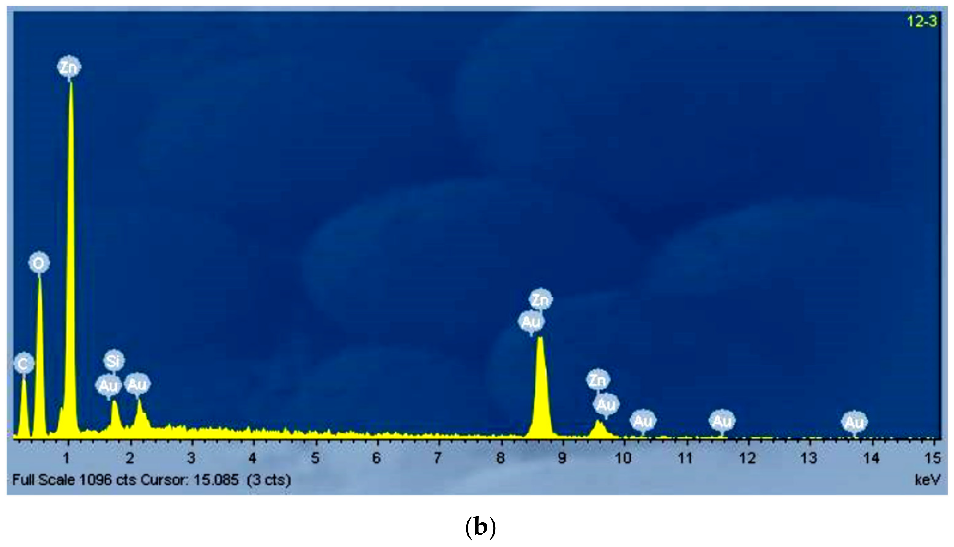
2.3. Characterization
3. Results and Discussion
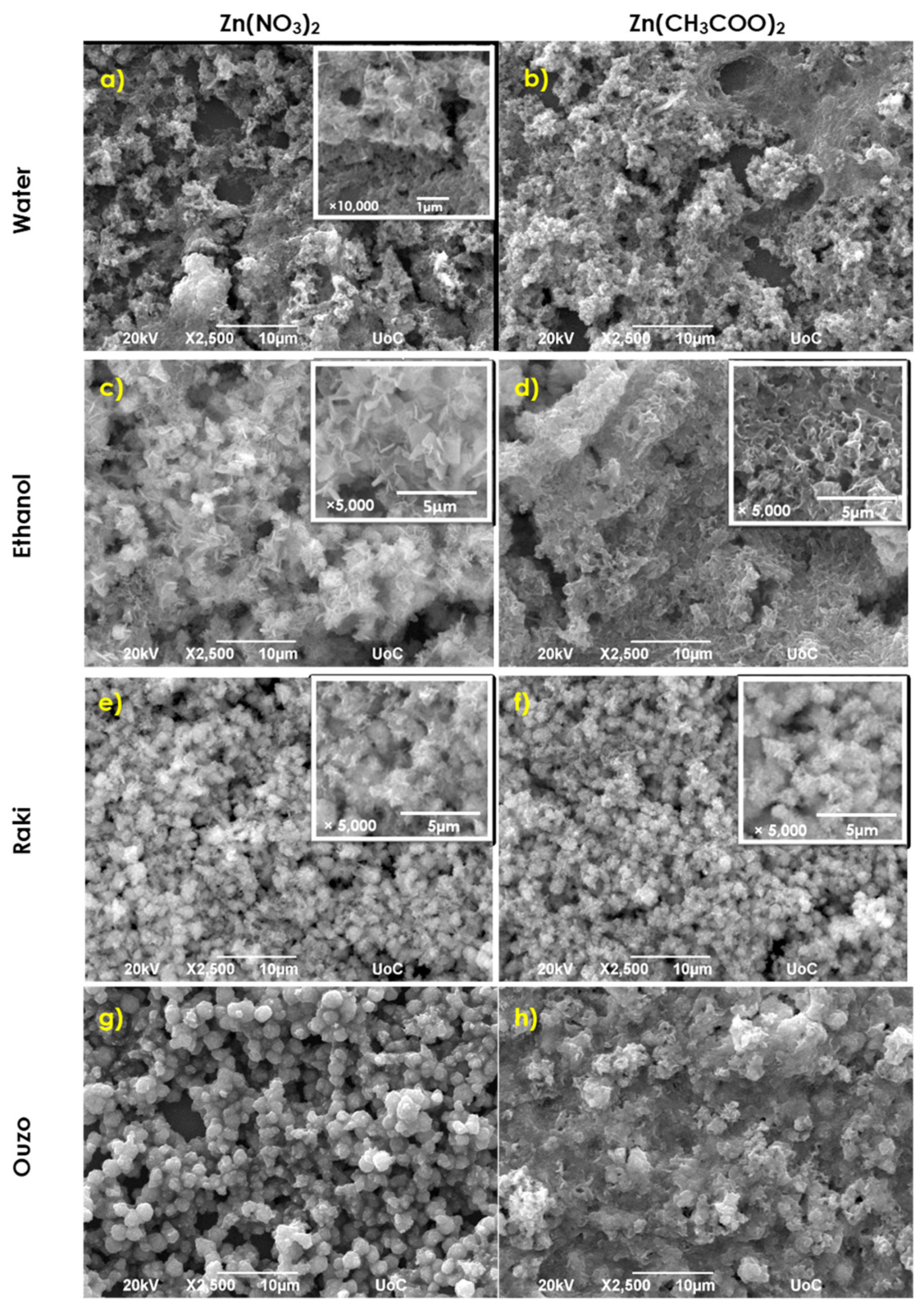
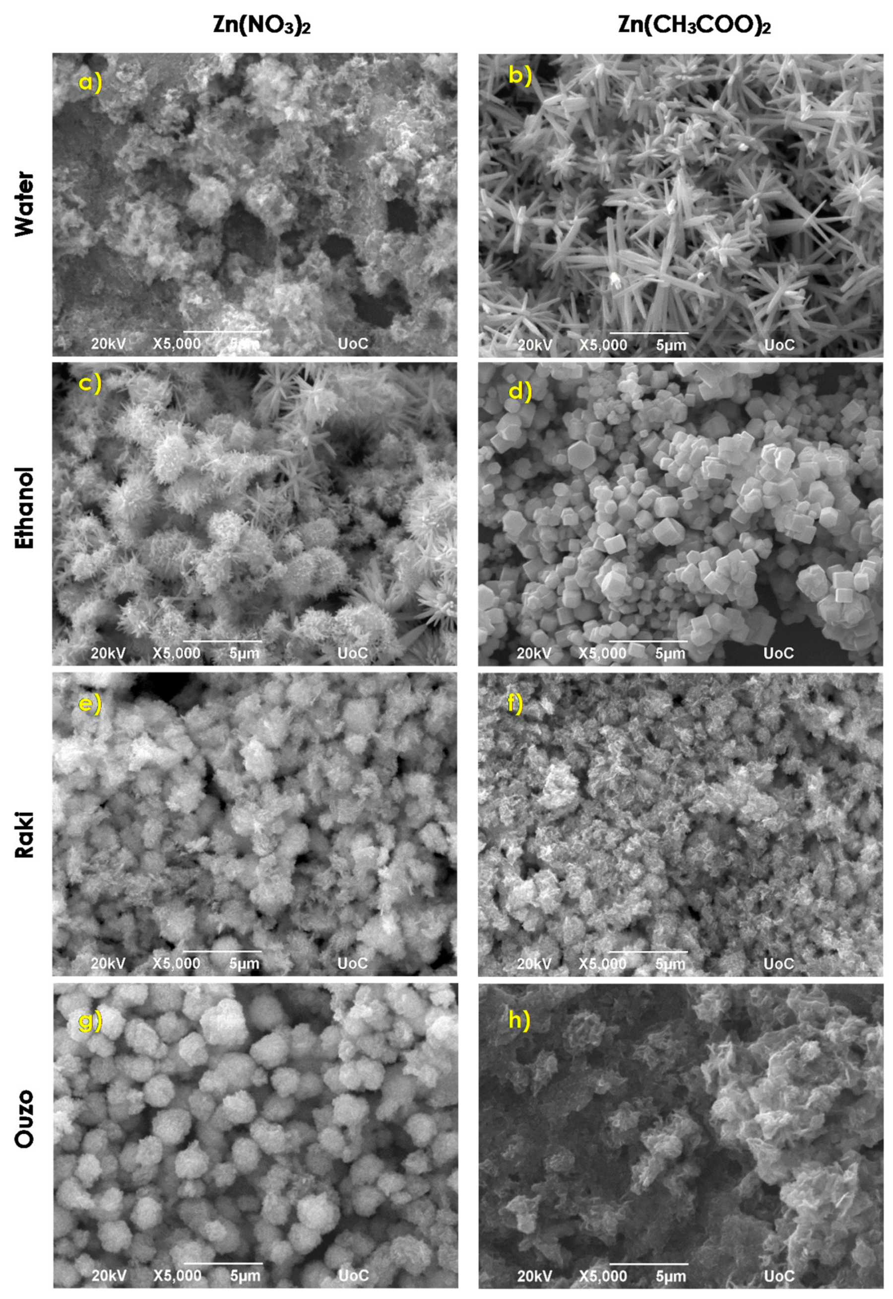
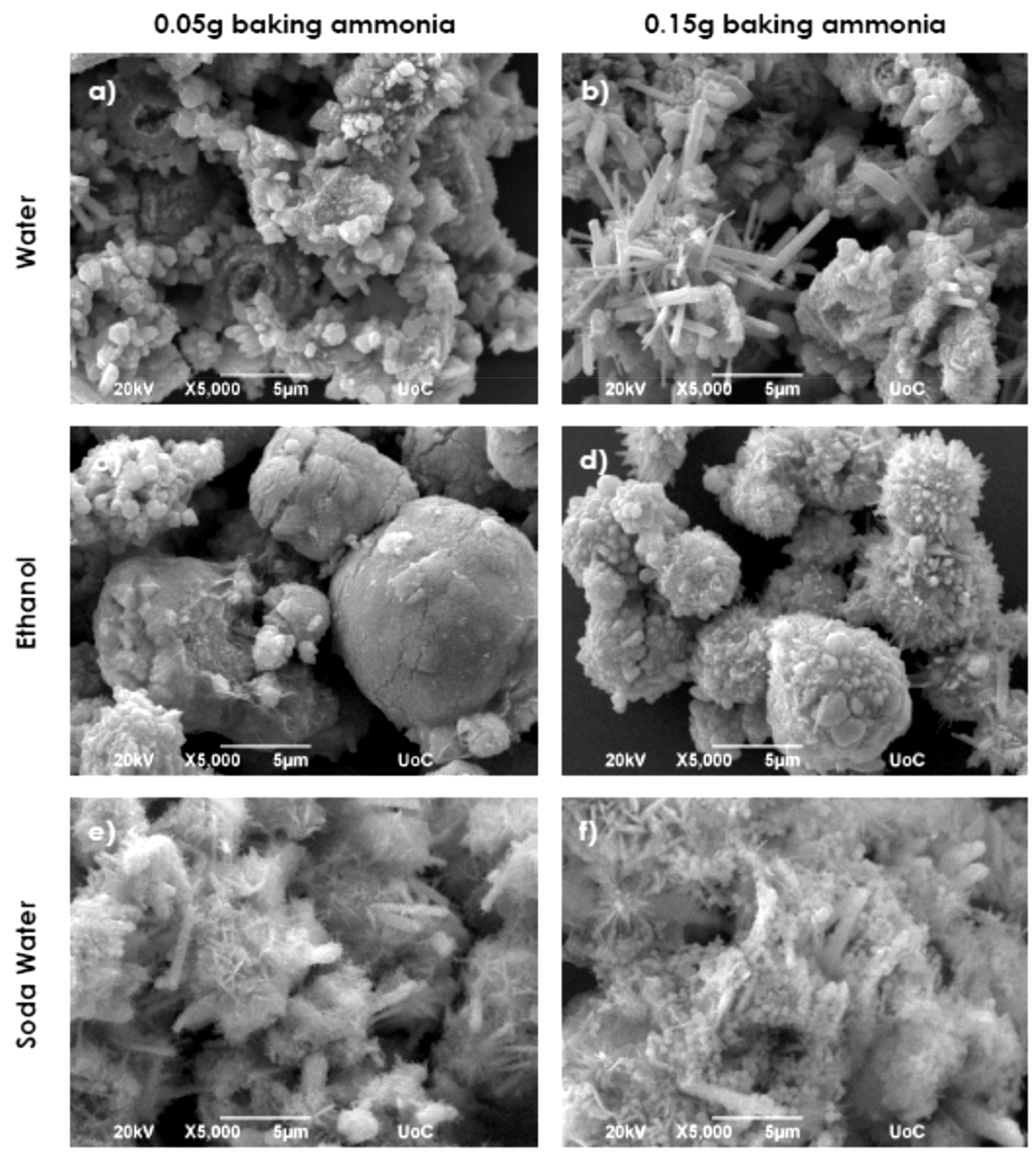
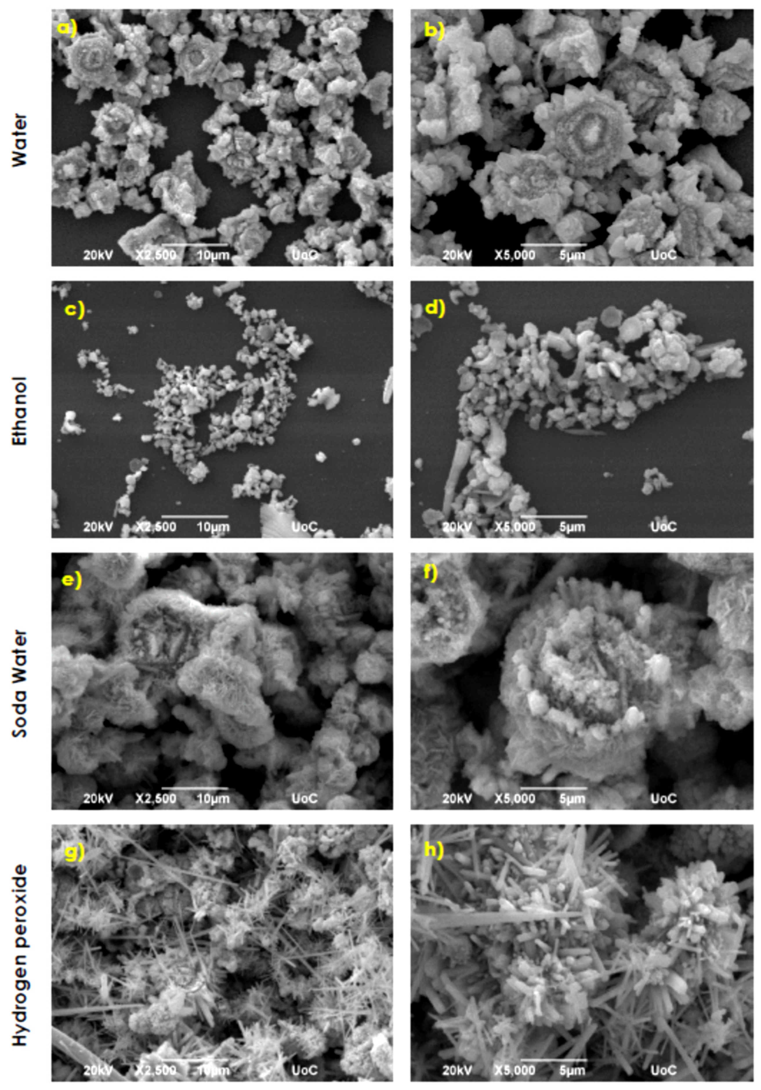
3.1. Growth and Structuring
Morphology and Structuring onto Si Substrates
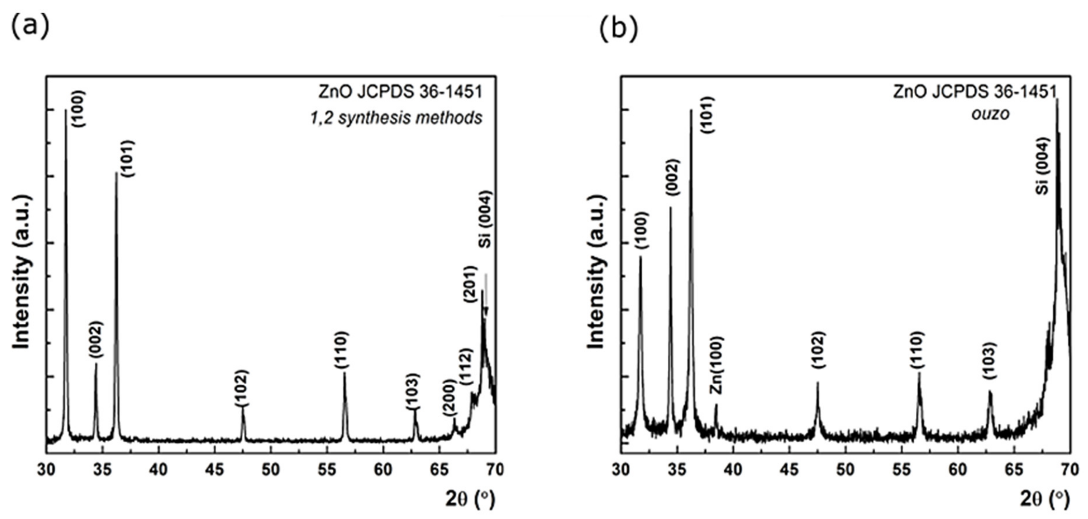
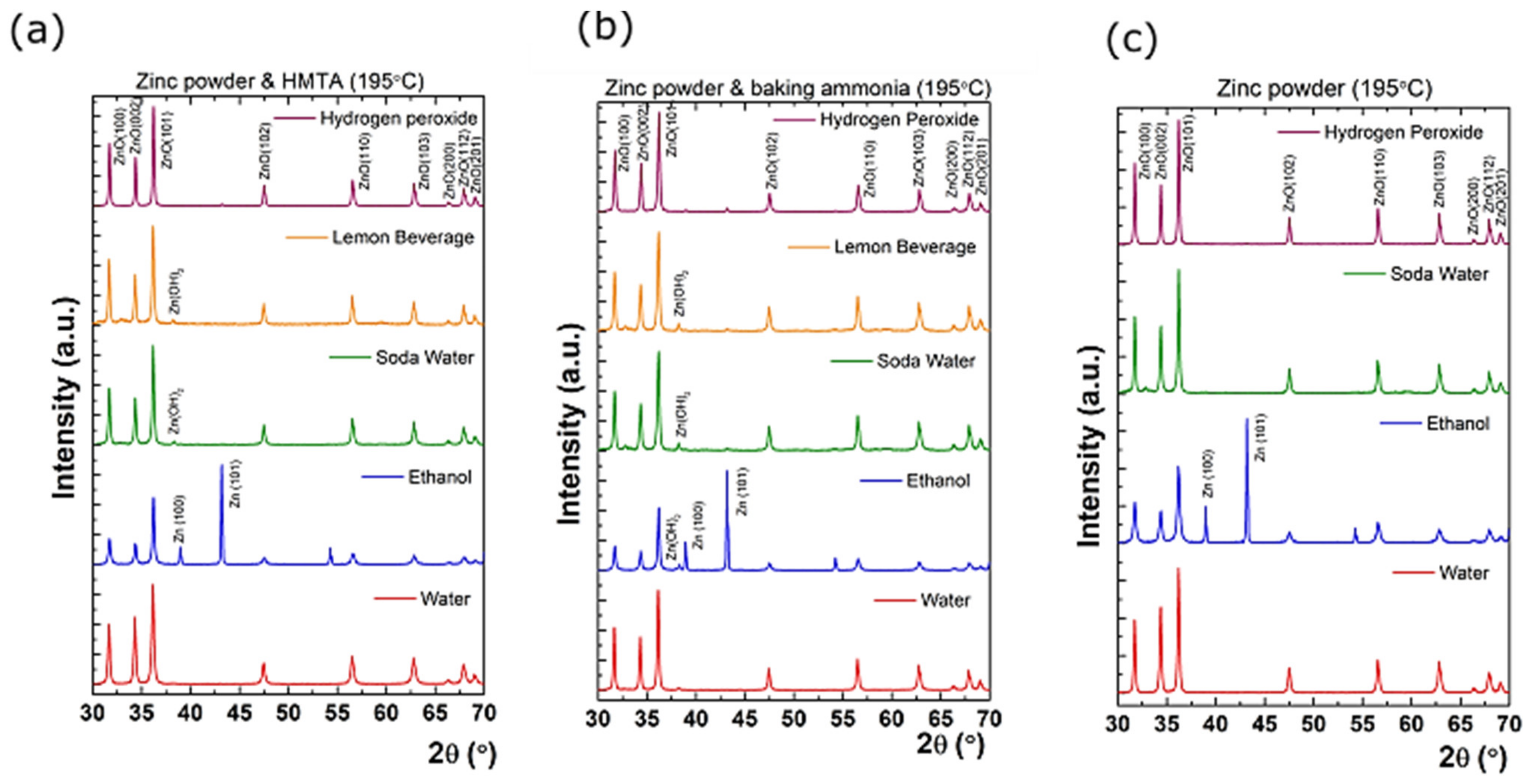
3.2. XRD Characterization
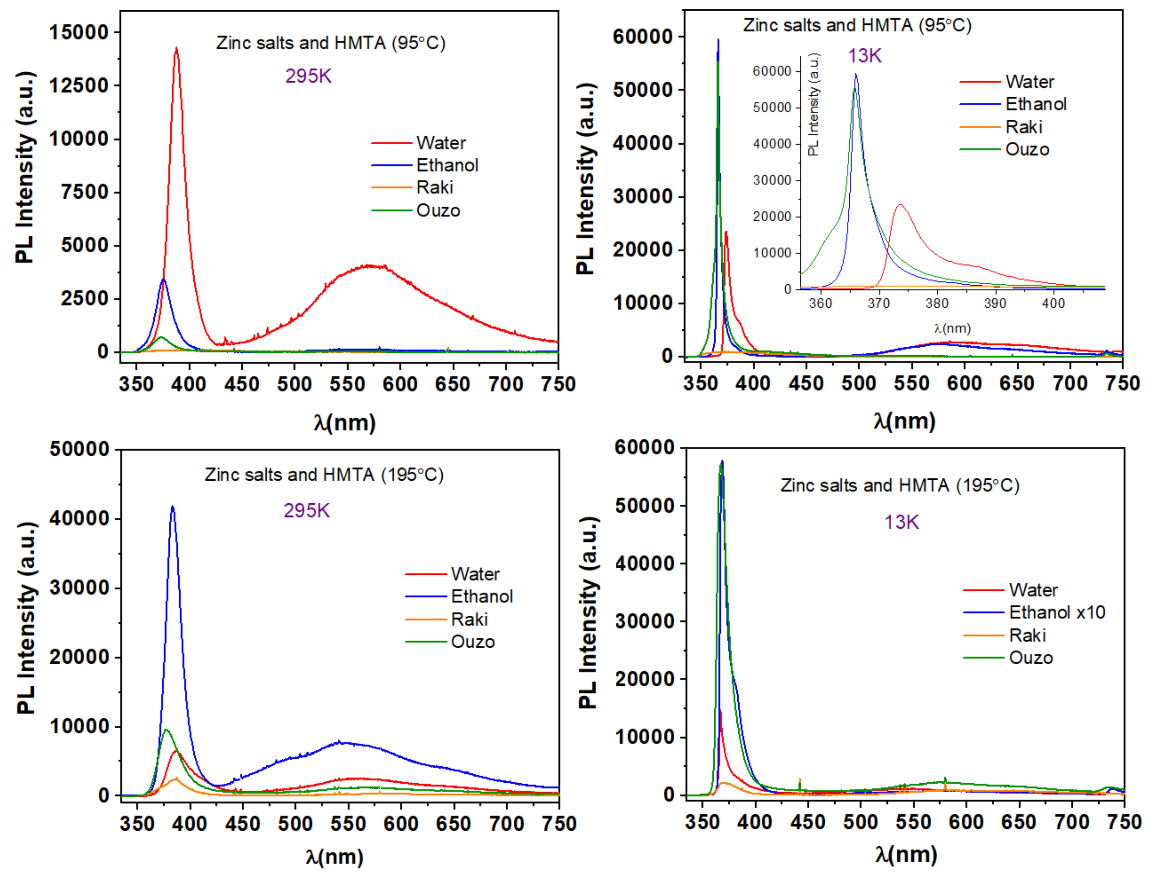
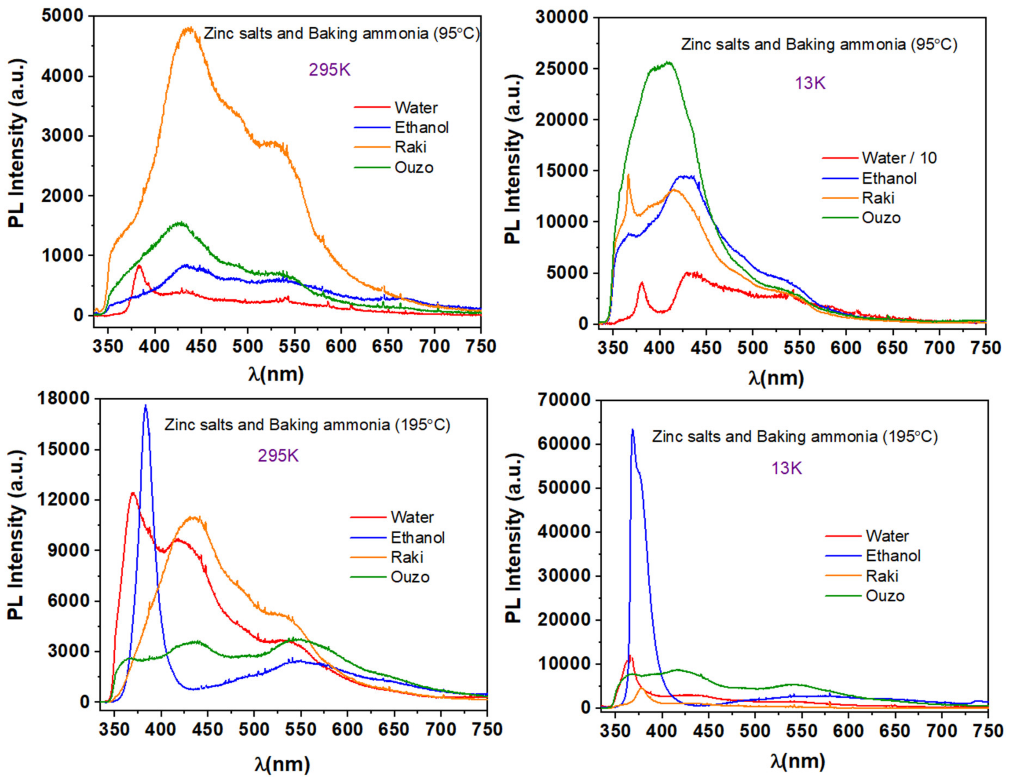
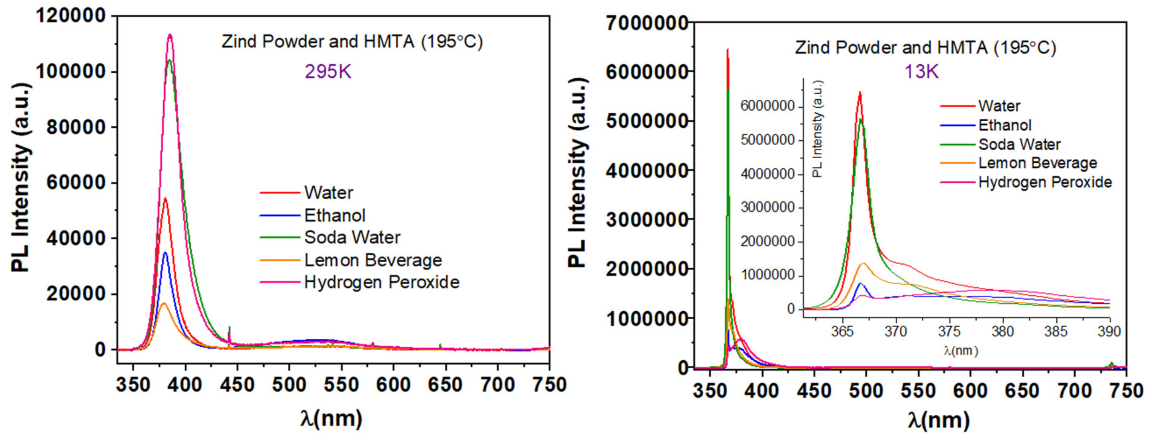
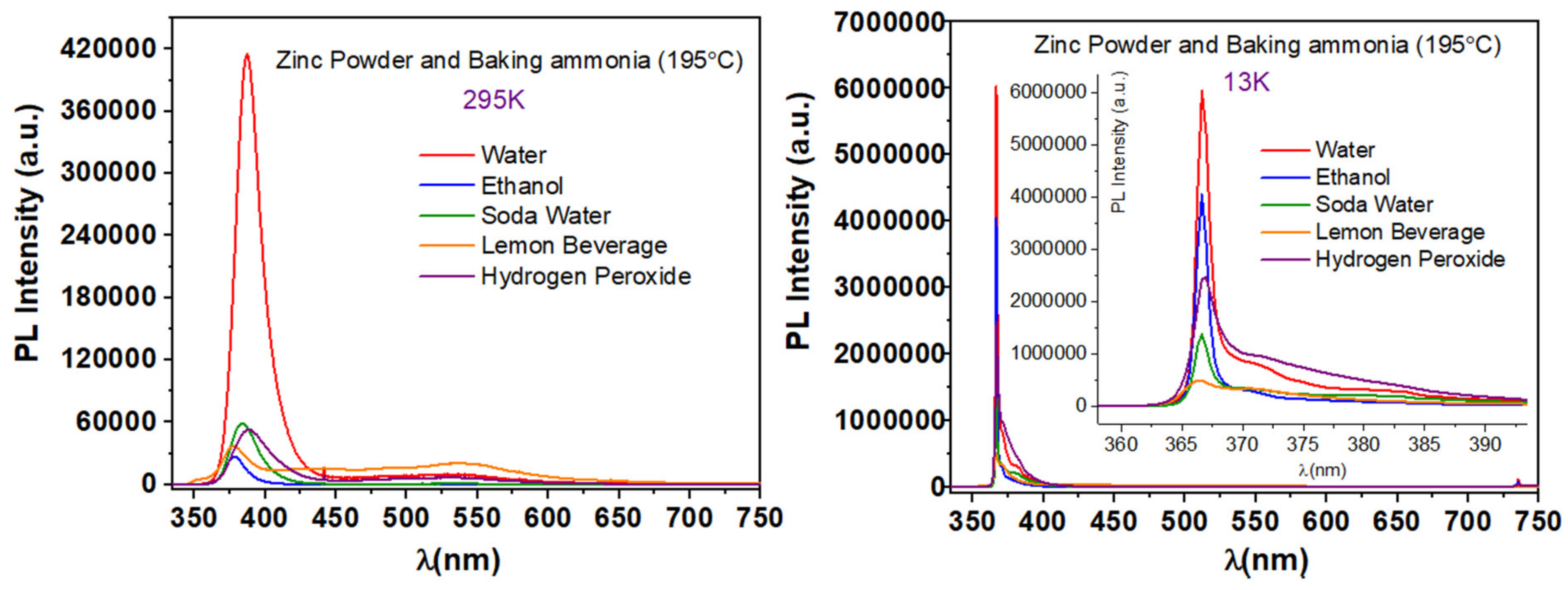
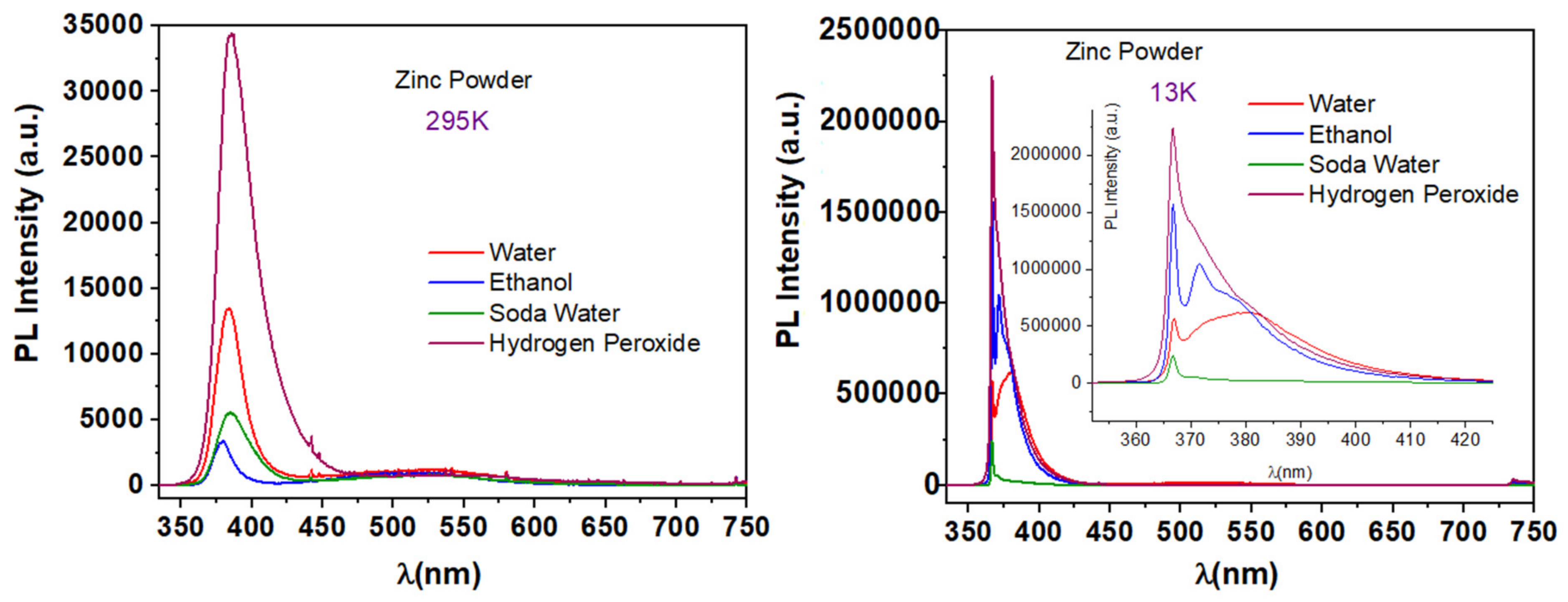
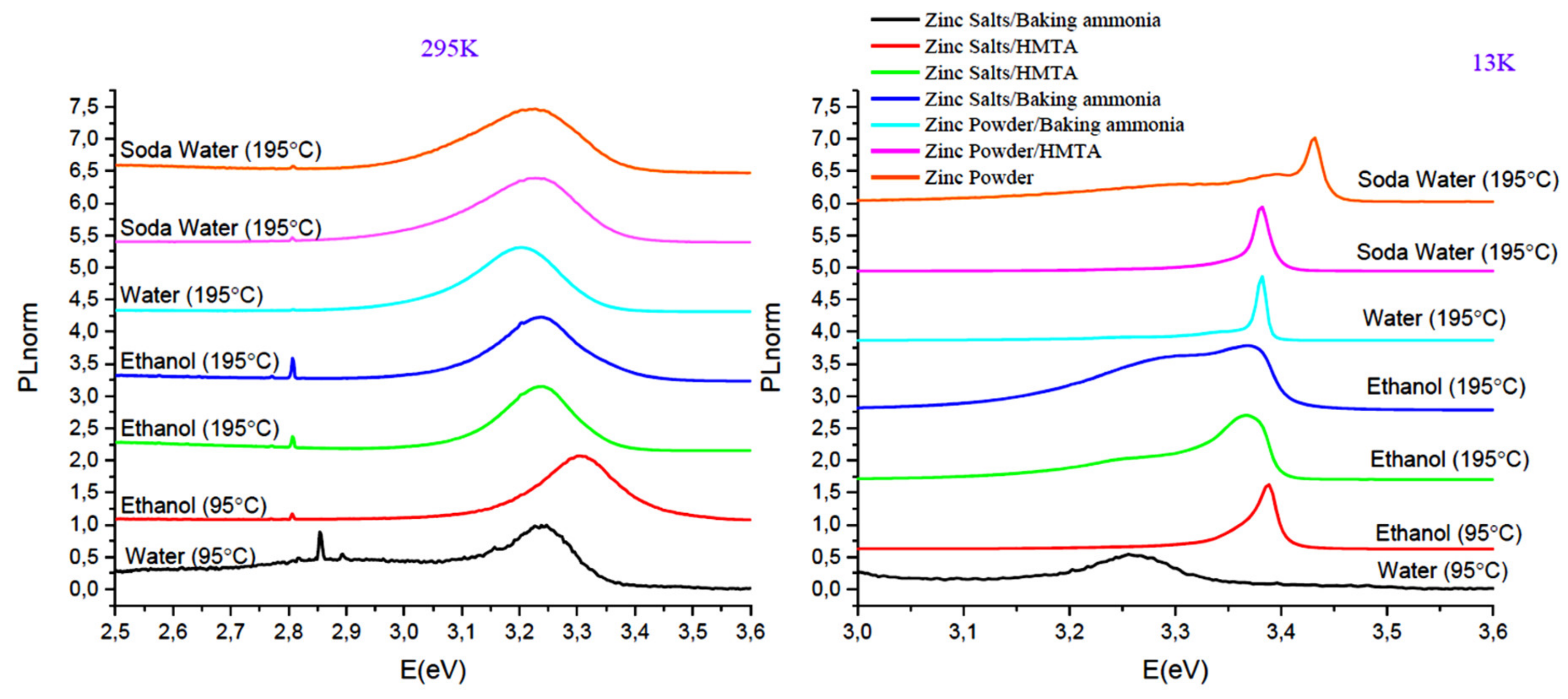
3.3. Photoluminescence Studies
- (1)
- (2)
- (3)
- The samples synthesized via synthesis route 9 (Figure 15) show QY values ranging from 3% up to 20%, with the better value corresponding to the sample prepared in soda water.
4. Conclusions
Supplementary Materials
Author Contributions
Funding
Institutional Review Board Statement
Informed Consent Statement
Data Availability Statement
Acknowledgments
Conflicts of Interest
References
- Klingshirn, C.; Fallert, J.; Zhou, H.; Sartor, J.; Thiele, C.; Maier-Flaig, F.; Schneider, D.; Kalt, H. 65 years of ZnO research—Old and very recent results. Phys. Status Solidi B 2010, 247, 1424–1447. [Google Scholar] [CrossRef]
- Özgür, U.; Alivov, Y.I.; Liu, C.; Teke, A.; Reshchikov, M.A.; Doğan, S.; Avrutin, V.; Cho, S.J.; Morkoç, H. A comprehensive review of ZnO materials and devices. J. Appl. Phys. 2005, 98, 041301. [Google Scholar] [CrossRef] [Green Version]
- Shahzad, S.; Javed, S.; Usman, M. A Review on Synthesis and Optoelectronic Applications of Nanostructured ZnO. Front. Mater. 2021, 8, 613825. [Google Scholar] [CrossRef]
- Rodrigues, J.; Fernandes, A.J.S.; Monteiro, T.; Costa, F.M. A review on the laser-assisted flow deposition method: Growth of ZnO micro and nanostructures. CrystEngComm 2019, 21, 1071–1090. [Google Scholar] [CrossRef]
- Znaidi, L. Sol–gel-deposited ZnO thin films: A review. Mater. Sci. Eng. B 2010, 174, 18–30. [Google Scholar] [CrossRef]
- Arya, S.; Mahajan, P.; Mahajan, S.; Khosla, A.; Datt, R.; Gupta, V.; Young, S.-J.; Oruganti, S.K. Review—Influence of Processing Parameters to Control Morphology and Optical Properties of Sol-Gel Synthesized ZnO Nanoparticles. ECS J. Solid State Sci. Technol. 2021, 10, 023002. [Google Scholar] [CrossRef]
- Hasnidawani, J.; Azlina, H.; Norita, H.; Bonnia, N.; Ratim, S.; Ali, E. Synthesis of ZnO Nanostructures Using Sol-Gel Method. Procedia Chem. 2016, 19, 211–216. [Google Scholar] [CrossRef] [Green Version]
- Harun, K.; Hussain, F.; Purwanto, A.; Sahraoui, B.; Zawadzka, A.; Mohamad, A.A. Sol–gel synthesized ZnO for optoelectronics applications: A characterization review. Mater. Res. Express 2017, 4, 122001. [Google Scholar] [CrossRef]
- Nowak, E.; Szybowicz, M.; Stachowiak, A.; Koczorowski, W.; Schulz, D.; Paprocki, K.; Fabisiak, K.; Los, S. A comprehensive study of structural and optical properties of ZnO bulk crystals and polycrystalline flms grown by sol-gel method. Appl. Phys. A 2020, 126, 552. [Google Scholar] [CrossRef]
- Marouf, S.; Beniaiche, A.; Guessas, H.; Azizi, A. Morphological, Structural and Optical Properties of ZnO Thin Films Deposited by Dip Coating Method. Mater. Res. 2017, 20, 88–95. [Google Scholar] [CrossRef] [Green Version]
- Haque, M.J.; Bellah, M.M.; Hassan, M.R.; Rahman, S. Synthesis of ZnO nanoparticles by two different methods & comparison of their structural, antibacterial, photocatalytic and optical properties. Nano Express 2020, 1, 010007. [Google Scholar]
- da Silva, E.C.; de Moraes, M.O.S.; Brito, W.R.; Passos, R.R.; Brambilla, R.F.; da Costa, L.P.; Pocrifka, L.A. Synthesis of ZnO nanoparticles by the sol-gel protein route: A viable and efficient method for photocatalytic degradation of methylene blue and ibuprofen. J. Braz. Chem. Soc. 2020, 31, 1648–1653. [Google Scholar] [CrossRef]
- Darshita, M.N.; Sood, R. Review on synthesis and applications of zinc oxide nanoparticles. Preprints 2021, 2021050688. [Google Scholar]
- Pomastowski, P.; Król-Górniak, A.; Railean-Plugaru, V.; Buszewski, B. Zinc Oxide Nanocomposites—Extracellular Synthesis, Physicochemical Characterization and Antibacterial Potential. Materials 2020, 13, 4347. [Google Scholar] [CrossRef] [PubMed]
- Kolodziejczak-Radzimska, A.; Jesionowski, T. Zinc Oxide—From Synthesis to Application: A Review. Materials 2014, 7, 2833–2881. [Google Scholar] [CrossRef] [Green Version]
- Amakali, T.; Daniel, L.S.; Uahengo, V.; Dzade, N.Y.; de Leeuw, N.H. Structural and Optical Properties of ZnO Thin Films Prepared by Molecular Precursor and Sol–Gel Methods. Crystals 2020, 10, 132. [Google Scholar] [CrossRef] [Green Version]
- Vernardou, D.; Kenanakis, G.; Couris, S.; Koudoumas, E.; Kymakis, E.; Katsarakis, N. pH effect on the morphology of ZnO nanostructures grown with aqueous chemical growth. Thin Solid Films 2007, 515, 8764–8767. [Google Scholar] [CrossRef]
- Available online: https://www.accessdata.fda.gov/scripts/cdrh/cfdocs/cfCFR/CFRSearch.cfm?fr=184.1137 (accessed on 1 March 2021).
- Available online: https://en.wikipedia.org/wiki/Ammonium_carbonate (accessed on 1 March 2021).
- Sevastaki, M.; Papadakis, V.M.; Romanitan, C.; Suchea, M.P.; Kenanakis, G. Photocatalytic Properties of Eco-Friendly ZnO Nanostructures on 3D-Printed Polylactic Acid Scaffolds. Nanomaterials 2021, 11, 168. [Google Scholar] [CrossRef]
- Sun, X.; Chen, X.; Deng, Z.; Li, Y. A CTAB-assisted hydrothermal orientation growth of ZnO nanorods. Mater. Chem. Phys. 2003, 78, 99–104. [Google Scholar] [CrossRef]
- Panchakarla, L.S.; Govindaraj, A.; Rao, C.N.R. Formation of ZnO Nanoparticles by the Reaction of Zinc Metal with Aliphatic Alcohols. J. Clust. Sci. 2007, 18, 660–670. [Google Scholar] [CrossRef]
- Zhao, A.; Luo, T.; Chen, L.; Liu, Y.; Li, X.; Tang, Q.; Cai, P.; Qian, Y. Synthesis of ordered ZnO nanorods film on zinc-coated Si substrate and their photoluminescence property. Mater. Chem. Phys. 2006, 99, 50–53. [Google Scholar] [CrossRef]
- Umar, A.; Kim, S.; Im, Y.; Hahn, Y. Structural and optical properties of ZnO micro-spheres and cages by oxidation of metallic Zn powder. Superlattices Microstruct. 2006, 39, 238–246. [Google Scholar] [CrossRef]
- Ma, Q.L.; Xiong, R.; Zhai, B.G.; Huang, Y.M. Water Assisted Conversion of ZnO from Metallic Zinc Particles. Key Eng. Mater. 2013, 538, 38–41. [Google Scholar] [CrossRef]
- Zhang, J.; Sun, L.; Yin, J.; Su, H.; Liao, C.; Yan, C. Control of ZnO morphology via a simple solution route. Chem. Mater. 2002, 14, 4172–4177. [Google Scholar] [CrossRef]
- Suchea, M.; Tudose, I.V.; Vrinceanu, N.; Istrate, B.; Munteanu, C.; Koudoumas, E. Precursor concentration effect on structure and morphology of ZnO for coatings on fabric substrates. Acta Chim. Iasi 2013, 21, 107–116. [Google Scholar] [CrossRef] [Green Version]
- Yin, J.; Gao, F.; Wei, C.; Lu, Q. Water Amount Dependence on Morphologies and Properties of ZnO nanostructures in Double-solvent System. Sci. Rep. 2014, 4, 3736. [Google Scholar] [CrossRef] [Green Version]
- Williamson, G.; Hall, W. X-ray line broadening from filed aluminium and wolfram. Acta Met. 1953, 1, 22–31. [Google Scholar] [CrossRef]
- Rahman, F. Zinc oxide light-emitting diodes: A review. Opt. Eng. 2019, 58, 010901. [Google Scholar] [CrossRef]
- Khranovskyy, V.; Lazorenko, V.; Lashkarev, G.; Yakimova, R. Luminescence anisotropy of ZnO microrods. J. Lumin. 2012, 132, 2643–2647. [Google Scholar] [CrossRef] [Green Version]
- Chen, X.-B.; Huso, J.; Morrison, J.L.; Bergman, L. The properties of ZnO photoluminescence at and above room temperature. J. Appl. Phys. 2007, 102, 116105. [Google Scholar] [CrossRef]
- Serrano, A.; Arana, A.; Galdámez, A.; Dutt, A.; Monroy, B.; Güell, F.; Santana, G. Effect of the seed layer on the growth and orientation of the ZnO nanowires: Consequence on structural and optical properties. Vacuum 2017, 146, 509–516. [Google Scholar] [CrossRef]
- Morkoc, H.; Özgür, Ü. Zinc Oxide: Fundamentals, Materials and Device Technology; John Wiley & Sons: Hoboken, NJ, USA, 2008; ISBN 978-3-527-62395-2. [Google Scholar]
- Jagadish, C.; Pearton, S. Zinc Oxide Bulk, Thin Films and Nanostructures; Elsevier B.V.: New York, NY, USA, 2006; ISBN 978-0-08-044722-3. [Google Scholar]
- Leiter, F.H.; Alves, H.R.; Hofstaetter, A.; Hofmann, D.M.; Meyer, B.K. The oxygen vacancy as the origin of a green emission in undoped ZnO. Phys. Status Solidi B 2001, 226, R4–R5. [Google Scholar] [CrossRef]
- Quemener, V.; Vines, L.; Monakhov, E.V.; Svensson, B.G. Evolution of deep electronic states in ZnO during heat treatment in oxygen- and zinc-rich ambients. Appl. Phys. Lett. 2012, 100, 112108. [Google Scholar] [CrossRef]
- Markus Raphael Wagner, Fundamental Properties of Excitons and Phonons in ZnO: A Spectroscopic Study of the Dynamics, Polarity, and Effects of External Fields. 2010. Available online: https://d-nb.info/1064813542/34 (accessed on 1 March 2021).


| Synthesis Method/Solvent | Mean Crystallite Size, d (nm) | Lattice Strain, ε (%) |
|---|---|---|
| Zn powder and HMTA/water | 37.4 | 0.18 |
| Zn powder and HMTA/ethanol | 33.6 | 0.23 |
| Zn powder and HMTA/soda water | 40.7 | 0.11 |
| Zn powder and HMTA/lemon beverage | 40.7 | 0.13 |
| Zn powder and HMTA/hydrogen peroxide | 49.5 | 0.17 |
| Zn powder and baking ammonia/water | 42 | 0.12 |
| Zn powder and baking ammonia/ethanol | 33.8 | 0.09 |
| Zn powder and baking ammonia/soda water | 37.4 | 0.11 |
| Zn powder and baking ammonia/lemon beverage | 36.3 | 0.11 |
| Zn powder and baking ammonia/hydrogen peroxide | 43.3 | 0.16 |
| Zn powder/water | 39.6 | 0.17 |
| Zn powder/ethanol | 29.4 | 0.15 |
| Zn powder/soda water | 40.7 | 0.14 |
| Zn powder/hydrogen peroxide | 44.7 | 0.12 |
Publisher’s Note: MDPI stays neutral with regard to jurisdictional claims in published maps and institutional affiliations. |
© 2021 by the authors. Licensee MDPI, Basel, Switzerland. This article is an open access article distributed under the terms and conditions of the Creative Commons Attribution (CC BY) license (https://creativecommons.org/licenses/by/4.0/).
Share and Cite
Suchea, M.P.; Petromichelaki, E.; Romanitan, C.; Androulidaki, M.; Manousaki, A.; Viskadourakis, Z.; Ikram, R.; Pascariu, P.; Kenanakis, G. Obtaining Nanostructured ZnO onto Si Coatings for Optoelectronic Applications via Eco-Friendly Chemical Preparation Routes. Nanomaterials 2021, 11, 2490. https://0-doi-org.brum.beds.ac.uk/10.3390/nano11102490
Suchea MP, Petromichelaki E, Romanitan C, Androulidaki M, Manousaki A, Viskadourakis Z, Ikram R, Pascariu P, Kenanakis G. Obtaining Nanostructured ZnO onto Si Coatings for Optoelectronic Applications via Eco-Friendly Chemical Preparation Routes. Nanomaterials. 2021; 11(10):2490. https://0-doi-org.brum.beds.ac.uk/10.3390/nano11102490
Chicago/Turabian StyleSuchea, Mirela Petruta, Evangelia Petromichelaki, Cosmin Romanitan, Maria Androulidaki, Alexandra Manousaki, Zacharias Viskadourakis, Rabia Ikram, Petronela Pascariu, and George Kenanakis. 2021. "Obtaining Nanostructured ZnO onto Si Coatings for Optoelectronic Applications via Eco-Friendly Chemical Preparation Routes" Nanomaterials 11, no. 10: 2490. https://0-doi-org.brum.beds.ac.uk/10.3390/nano11102490