
Thin-Film Solar Cells Based on Selenized CuSbS2 Absorber
by
 , ,
, ,
Minghao Zhao
1,2, 
Junsheng Yu
1,
Lijuan Fu
1,2,
Youwei Guan
2,*,
Hua Tang
2,
Lu Li
1,2 and
Jiang Cheng
1,2,* 1
School of Optoelectronic Science and Engineering, University of Electronic Science and Technology of China (UESTC), Chengdu 610054, China
2
Co-Innovation Center for Micro/Nano Optoelectronic Materials and Devices, Chongqing University of Arts and Sciences, Chongqing 402160, China
*
Authors to whom correspondence should be addressed.
Nanomaterials 2021, 11(11), 3005; https://0-doi-org.brum.beds.ac.uk/10.3390/nano11113005
Submission received: 28 September 2021
/
Revised: 5 November 2021
/
Accepted: 6 November 2021
/
Published: 9 November 2021
(This article belongs to the Special Issue State-of-the-Art Nanophotonic and Optical Nanomaterials in China)
Abstract
:Copper antimony sulfide (CuSbS2) has attracted significant interest as an earth-abundant photovoltaic absorber. However, the efficiency of the current CuSbS2 photovoltaic device is too low to meet the requirement of a large-scale application. In this study, selenylation was introduced to optimize the band structure and improve the device performance. Selenized CuSbS2 [CuSbS2(Se)] films were realized using porous CuSbS2 films prepared by spray deposition with a post-treatment in Se vapor. The as-prepared CuSbS2(Se) films exhibited a compact structure. X-ray diffraction and elemental analysis confirmed the effective doping of Se into the lattice by substituting a part of S in CuSbS2. Elemental analysis revealed a gradient distribution for Se from the top surface to the deeper regions, and the substitution rate was very high (>39%). Dark J–V characteristics and AC impedance spectroscopy analysis showed that selenylation significantly reduced the carrier recombination center. As a result, the selenized CuSbS2 device exhibited a significant efficiency improvement from 0.12% to 0.90%, which is much higher than that of the simply annealed device (0.46%), indicating this technique is a promising approach to improve the performance of CuSbS2 solar cells.
1. Introduction
To cope up with the challenges brought by increasing global energy consumption and pollution caused by fossil fuel consumption, the utilization of solar energy such as the photovoltaic technique has received extensive research attention for a long time [1,2]. In the last decade, inorganic thin-film solar cells have achieved a great height via material innovation and technical improvement. Cadmium telluride (CdTe) and copper–indium–gallium–selenium (CIGS) thin-film solar cells have achieved tremendously high efficiency of >21% [3,4]. The rapid transcendence of organic–inorganic metal halide perovskite solar cells to above 25% efficiency mark has captivated the significant attention of the photovoltaic research community [5,6]. Very recently, Hou’s group reported the preparation of organic solar cells with a certified 19.6% high efficiency via the tandem technique, representing that the breakthrough of 20% efficiency for organic solar cells is simply a matter of time [7]. Nevertheless, this achievement does not indicate that most problems of larger-scale application have been well solved. Instead, many scientists still thrive on overcoming the obstacles of stability and lifetime of existing high-efficiency devices or seeking new high efficiency, environmentally friendly, and chemically stable photovoltaic materials.
Antimony chalcogenides, including Sb2Se3, Sb2S3, and Sb2(S1−xSex)3, have attracted significant research attention as a new group of absorber materials that meet the most requirements for large-scale application, in particular, the chemical stability and raw materials source aspects [8,9,10,11,12,13,14]. Unencapsulated devices based on antimony chalcogenides remain nearly undegraded after two months in ambient air. They can even work fine in damp–heat conditions (85 °C, 85% humidity). For example, the Sb2(S1−xSex)3 device prepared by spray pyrolysis exhibited an efficiency degradation of only less than 6% in that condition. Through years of continuous efforts and development, the best power conversion efficiency (PCE) of antimony chalcogenides-based devices has exceeded 10%, indicating it has great potential as an alternative next-generation solar cell material.
Copper antimony chalcogenides, such as CuSbS2, CuSbSe2, and CuSb(S,Se)2 have also been considered as the promising photovoltaic absorbers due to their tunable energy bandgap of 1.45–1.08 eV, switchable hole concentrations of 1016–1018 cm−3, and hole mobility of 0.1–1.0 cm2 V−1 S−1 [15]. Copper antimony chalcogenides consist of a cleavage-free chalcostibite structure. The devices exhibit very high stability, which is even better than that of antimony chalcogenides. Comparative analysis indicates that antimony chalcogenides have a layered stibnite structure in which the ribbons stacked perpendicular to [001] direction are held together by the weak van der Waals forces, which could undoubtedly bring unstable factors [16,17]. Unfortunately, most copper antimony chalcogenide solar cells have suffered from poor (<4%) efficiencies, which is far from its spectroscopic-limited maximum efficiency (22.9%) [1,18]. However, some limiting factors for the unexpected low efficiencies have become progressively clearer after years of research efforts. The interface problems such as ohmic contacts [19] and band offset [20,21] between the CuSbS2 and CdS buffer layer have been excessively discussed. In our previous study, it was found that crystal defects and atomic disorders could also bring serious recombination [22]. Although the PCE of the CuSbS2 device was improved from 0.73% to 2.48% by introducing Ag atoms into CuSbS2 crystal structure, there still existed many unsettled problems. For example, the energy band (Eg) of CuSbS2 of 1.58 eV is a little larger for an efficient solar cell. The current density (JSC) was restricted to a very low level due to the narrow absorption range (350–600 nm) and the poor carrier transport capacity was encountered.
Herein, in order to improve the performance of CuSbS2 devices, selenylation treatment was taken into account. High-quality CuSbS2(Se) thin films were successfully realized by the previously used spray pyrolysis-selenylation (SPS) method. This routine was selected herein because spray-coated CuSbS2 films may possess a better porosity that could make selenylation easier and create a higher-quality CuSbS2(Se) film than that prepared by other methods. As expected, the selenized CuSbS2 absorbers exhibited obvious optimized optical and electrical properties, bringing a significant improvement of PCE from 0.12% to 0.90%, which is obviously higher than that treated in N2 at the same temperature. Although the progress is not significant, this method has been proven to be very effective in improving CuSbS2 solar cells.
2. Materials and Methods
2.1. Chemicals
Copper acetate monohydrate (C4H6CuO4·H2O, 99.95%), antimony acetate (C6H9O6Sb, 99.99%), thiourea (CH4N2S, 99%), glycol methyl ether (C3H8O2, 99.5%), and selenium powder were purchased from Macklin Inc. (Shanghai, China).
2.2. Preparation of CuSbS2(Se) Method
CuSbS2(Se) was prepared by the previously reported SPS method, i.e., CuSbS2 was first prepared by spray pyrolysis deposition (SPD) and then selenized in Se vapor. For the SPD of CuSbS2, the spray solution was prepared by dissolving copper acetate monohydrate (0.120 g, 0.6 mmol), antimony acetate (0.179 g, 0.6 mmol) and thiourea (0.190 g, 2.5 mmol) in glycol methyl ether (10 mL). To prevent precipitation, copper acetate monohydrate and antimony acetate should be respectively dissolved in glycol methyl ether at first. Further several drops of acetic acid (0.3 mL) should be added to the solution to inhibit hydrolysis.
In CuSbS2 deposition processing, the spray solution atomization rate was accurately tuned at 0.3 mL min−1, while the carrier gas (N2) was introduced at a flow rate of 20 L min−1, and the substrate temperature was maintained at 350 °C. The deposition rate of CuSbS2 films was about 100 nm min−1. Then, the prepared CuSbS2 films were transferred to a controlled dual-temperature zone RPT furnace. The selenylation process was fine-tuned to a condition where Se powder was maintained at 350 °C and the temperature of CuSbS2-coated wafer was maintained at 400 °C.
2.3. Device Fabrication
Indium tin oxide (ITO) coated glasses with a nominal sheet resistance of 7 Ω were used as substrates for coating fabrication. All the substrates were cleaned with alkaline detergent (RM10-07, Rigorous Co., Ltd., Shenzhen, China) in an ultrasonic bath prior to their use. A cadmium sulfide (CdS, 100 nm) thin film was deposited on ITO by the widely used chemical bath deposition (CBD) technique. Then, a 1200 nm thick CuSbS2 thin film was deposited on the CdS buffer layer by SPD. Next, the CuSbS2 thin film was selenized in the RPT furnace for several minutes. Finally, 60 nm-thick Au back-contact electrodes were sputtered onto the top of CuSbS2(Se) in a DC sputtering coater.
2.4. Films Characterization and Device Testing
The composition and crystal structure were characterized by X-ray diffraction (XRD, AXS D8 Advance, Bruker, Karlsruhe, Germany). The film morphologies were characterized by scanning electron microscopy (SEM, Merlin, Zeiss, Oberkochen, Germany). Optical transmittance spectra of the blend films were obtained using an ultraviolet–visible–infrared (UV–vis–IR) spectrophotometer (Cary 5000, Agilent, Santa Clara, CA, USA). The electronic structure and energy level films were analyzed by X-ray photoelectron spectroscopy and UV photoelectron spectroscopy (XPS and UPS, respectively, ESCALAB 250xi, ThermoFisher, Waltham, MA, USA). The thickness of the films was measured using a stylus profile meter (Alpha-Step D-100, KLA-Tencor, Milpitas, CA, USA).
The current density–voltage (J–V) characteristics were measured using a Keithley 2400 SourceMeter, under the illumination of a xenon lamp (94043A, Newport, Rhode Island, USA) with a power of 100 mW cm−2. External quantum efficiency (EQE) was measured using an integrated system (7-SCSpecIII, Beijing SOFN, Beijing, China) with a lock-in amplifier under short-circuit conditions. Carrier transporting behavior was investigated by electrochemical workstation (CHI760e, Chenhua, Shanghai, China) under a suitable open-circuit voltage.
3. Results and Discussions
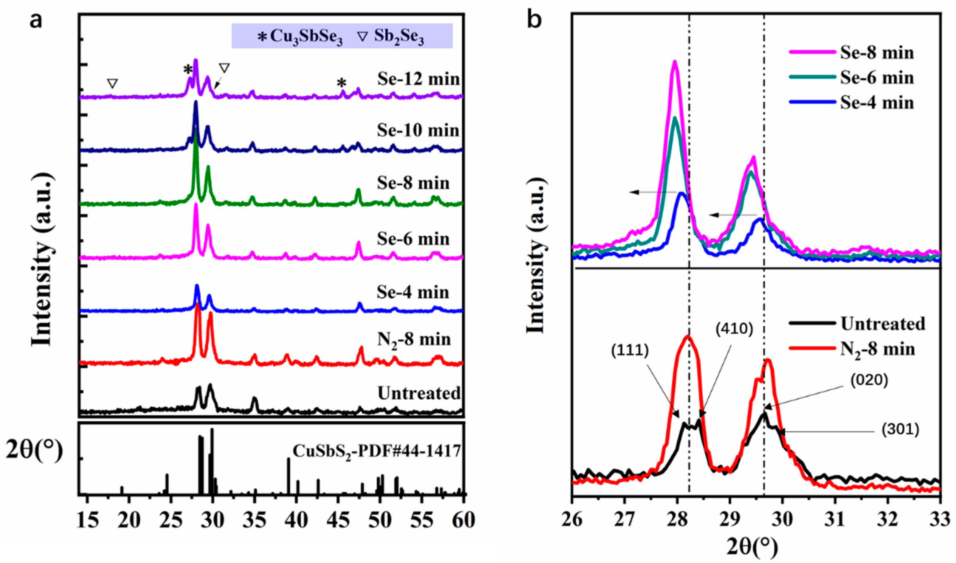
The formation of CuSbS2(Se) thin films was largely dependent on the quality of CuSbS2 thin films and the selenylation process. Moreover, the selenylation should bring multidimensional effects on the absorber and devices. Before the device analysis, the crystal structure and morphologies of selenized CuSbS2 were first investigated. The composition and phase information of CuSbS2(Se) selenized for different durations were confirmed by XRD. Figure 1a shows the XRD patterns of seven films subjected to different treatments. The XRD pattern of the untreated sample, in general, matched that of chalcostibite CuSbS2 (JCPDS No. 44-1417). The amorphous-like XRD peaks reflect its poor crystallinity. The sample heated in N2 at 400 °C for 8 min shows a higher intensity, indicating that a post-annealing for SPD prepared CuSbS2 is necessary. The samples selenized at 400 °C for a short time (~8 min) show a spectrum similar to that treated in N2. However, when the selenylation duration was prolonged to 10 and 12 min, Cu3SbSe3 and Sb2Se3 impurities peaks could be clearly observed. Similar to the other selenized absorbers, CuSbS2(Se) is unstable in Se-rich conditions and the selenylation duration should be controlled at a reasonable range [23,24]. Figure 1b shows the magnified view of the XRD peaks at 26–33°. The peaks centered at low 2θ correspond to the combination of (111) and (410) planes and the other peaks centered at higher 2θ indicate a combination of (020) and (301) planes. The two peaks exhibit a significant enhancement in intensity, but no obvious shift is observed before and after treatment in N2. For the selenized samples, all the four peaks gradually shift to lower 2θ with increasing full width at half maximum (FWHM) with the increase in the selenylation duration from 4 to 8 min, indicating the successful accessibility of Se to the crystal lattice.
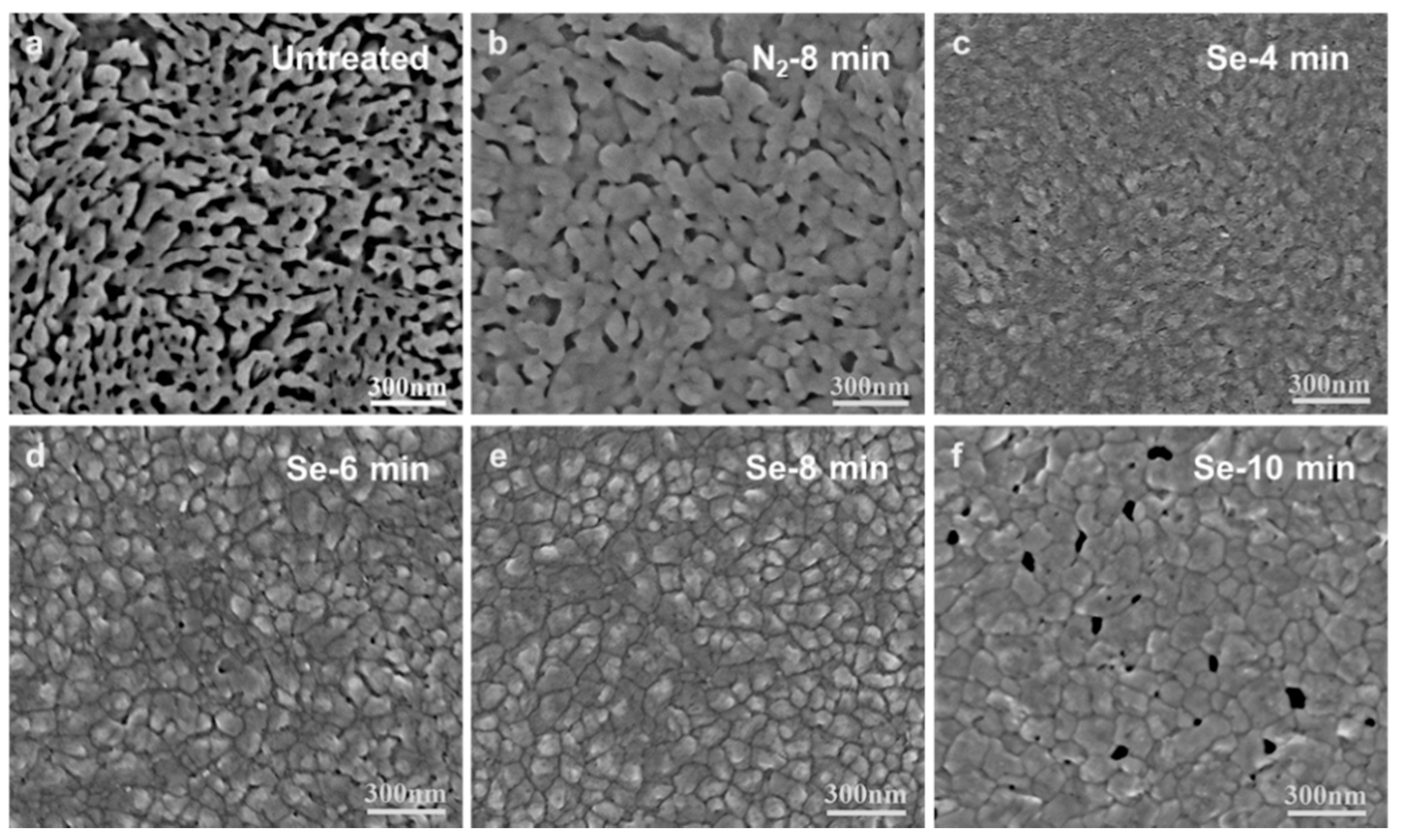
Surface morphologies further revealed the variation of chemical and crystal structure that was affected by post-treatment. Figure 2 shows the top SEM image of untreated CuSbS2 thin films and CuSbS2 treated in N2 and Se vapor for varied duration. The untreated films (Figure 2a) exhibit a porous and incompact structure. This loose texture provided a large reaction contact area. In contrast, the selenylation reaction level could be largely restricted by the compact structure of film because it was not so easy for the Se element to transport from the surface to the deeper regions. For example, selenized Sb2S3 devices that are prepared by thermal evaporation always exhibit much lower PCE than those obtained by solution method because of their compact surface and big crystal grains [11,23,25]. Figure 2b shows the surface of the sample treated in N2 for 8 min. Both the size and density of pores decreased, and grains were found to be bonded to each other in all ranges. With 4–6 min selenylation time, no big pores could be found anywhere. The crystal grains grew bigger and the boundary gradually became more and more distinct when the selenylation duration prolonged from 4 to 8 min. It also indicates that the crystallinity of CuSbS2 thin films could be improved by the heat treatment at 400 °C [26,27], which agrees well with the XRD results. The films selenized for 8 min showed a smooth and compact surface with an average grain size of about 70 nm. However, when increasing the selenylation duration (>12 min), pinholes could be found everywhere, which could lead to serious short circuits in devices.
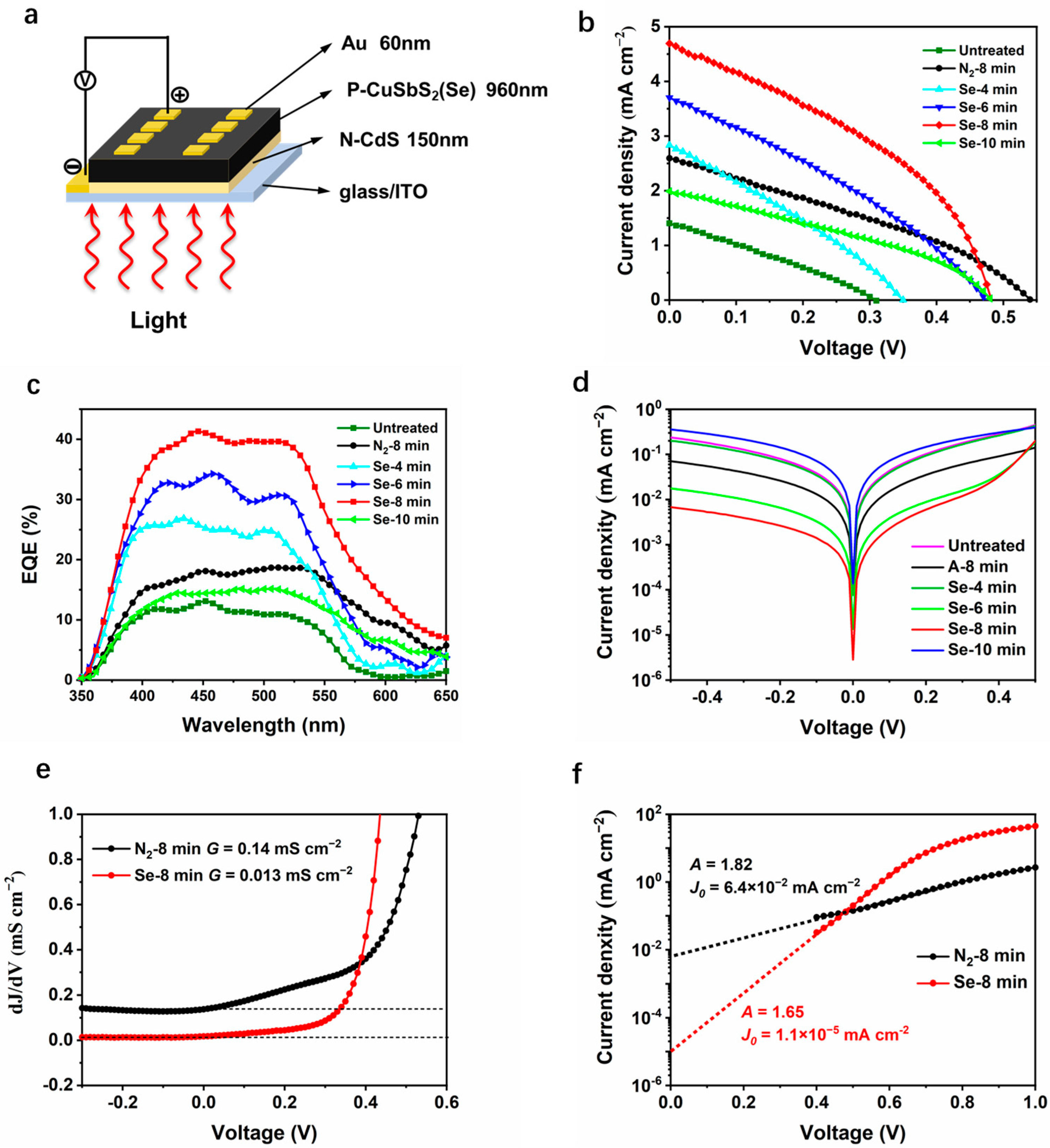
To evaluate the performance of CuSbS2(Se) thin films as absorbers, solar cells with a simple structure of ITO/CdS/CuSbS2(Se)/Au were prepared, and its sketch is illustrated in Figure 3a. Each specimen consists of eight devices with an active area of 0.04 cm2. All the specimens were tested under the same conditions. The current density–voltage (J–V) characteristics and external quantum efficiency (EQE) curves of the devices prepared by different treatments are shown in Figure 3b,c, and their performance details are presented in Table 1. The devices with untreated CuSbS2 absorber exhibit a VOC of 0.31 V, a JSC of 1.41 mA cm−2, and a fill factor (FF) of 0.28, resulting in a very low average PCE of 0.12%. The devices with absorbers heated in N2 exhibit better performance than the untreated devices due to the improvement of crystallinity. The PCE increases to 0.46 ± 0.05% with a much higher VOC of 0.54 V and a JSC of 2.6 mA cm−2. Overall, all the devices using selenized absorbers show varying degrees of enhancement in photovoltaic performance. With 4-min slight selenylation, the JSC and VOC increased to 2.83 mA cm−2 and 0.35 V, respectively. The device with optimum performance was obtained when the absorbers were selenized for 8 min. The highest PCE of 1.04% was achieved with a high JSC of 5.31 mA cm−2. When the selenylation duration was prolonged to 10 min, PCE further reduced to 0.31 ± 0.17% with a much lower JSC and a poor yield. When the selenylation duration was lengthened to 12 min or longer, few available devices were detected from J–V characteristics curve. This degradation could be caused by pinholes or even cracks as shown in Figure 2f. The same situation existed in selenized Sb2S3 and AgSbS2 devices [23,24]. The morphology damage could be related to Ostwald ripening, as the distribution of the Se element occurs faster than that of the S element. Thus, the selenylation temperature and duration for CuSbS2 film should be accurately controlled (e.g., 6–8 min in this condition).
EQE can provide more information about the photo-response for devices using CuSbS2 that are treated under different atmospheres and for different durations [28]. The devices with untreated CuSbS2 absorber exhibit a low EQE (>10%) with a narrow photoresponse range of 350–600 nm. With the increase in the selenylation duration from 4 to 8 min, the devices show increasing EQE from 15% to 40%, which agrees well with the JSC trend. The edge of the photo-response range shows a slight increase from 600 nm to more than 650 nm. Noteworthy, the EQE of CuSbS2 devices treated in N2 is obviously broader than those of untreated CuSbS2 devices and devices selenized for a short time (<6 min), although its EQE is even lower than the devices selenized for 4 min. It indicates that the low EQE at long wavelength range (600–650 nm) for devices using untreated CuSbS2 film and CuSbS2(Se) films selenized for a short time, is caused by interfacial carrier combining probably with the low crystallinity because the energetic photons are largely absorbed near the CdS/CuSbS2 interface [26].
To further reveal the mechanisms of selenized devices, dark J–V characteristics were investigated for devices subjected to different treatments. Figure 3d demonstrates that the devices selenized for 8 min show the lowest leakage current, illustrating its low charge carrier recombination. Through closer observation, the device treated in N2 exhibits a higher leakage current, although they have a similar crystallinity as selenized devices. To further explore the device physics, shunt conductance (G), series resistance (R), diode ideality factor (A), and reverse saturation current density (J0) of devices treated in N2 and Se vapor were calculated according to the general single exponential diode equations [29] presented below:
where JL is photocurrent density, k is Boltzmann constant, T is temperature, Rs is the series resistance, Rsh is the shunt resistance, and G = 1/Rsh is the shunt conductance. The direct plot of dJ/dV against V is presented in Figure 3e, where the G values obtained were 0.14 and 0.013 mS cm−2 for devices treated in N2 and Se vapor, respectively, by reading from the flat regions under reverse bias. The J0 values could be determined by the extended line of the linear region at 0 V, and the A values were obtained by the slopes of the lines. Figure 3f exhibits that the selenized devices have a very low J0 value of 1.1 × 10⁻⁵ mA cm−2 compared to the devices heated in N2 (6.4 × 10⁻² mA cm−2), confirming its significant low carrier recombination. The A value can reflect the main recombination region in the p–n junction. For an ideal p–n junction, A value is 1. Both the devices treated in N2 and Se vapor show A values between 1 and 2, indicating the main recombination occurs at the space charge region. For a selenized device, a smaller A value (1.65) represents that the absorber has a much lower trap density. Compared with devices heated in N2, the electrical improvement herein should be attributed to the variation of composition and crystal structure, accompanied by an essential improvement in the carrier concentration and carrier transport efficiency for the films.
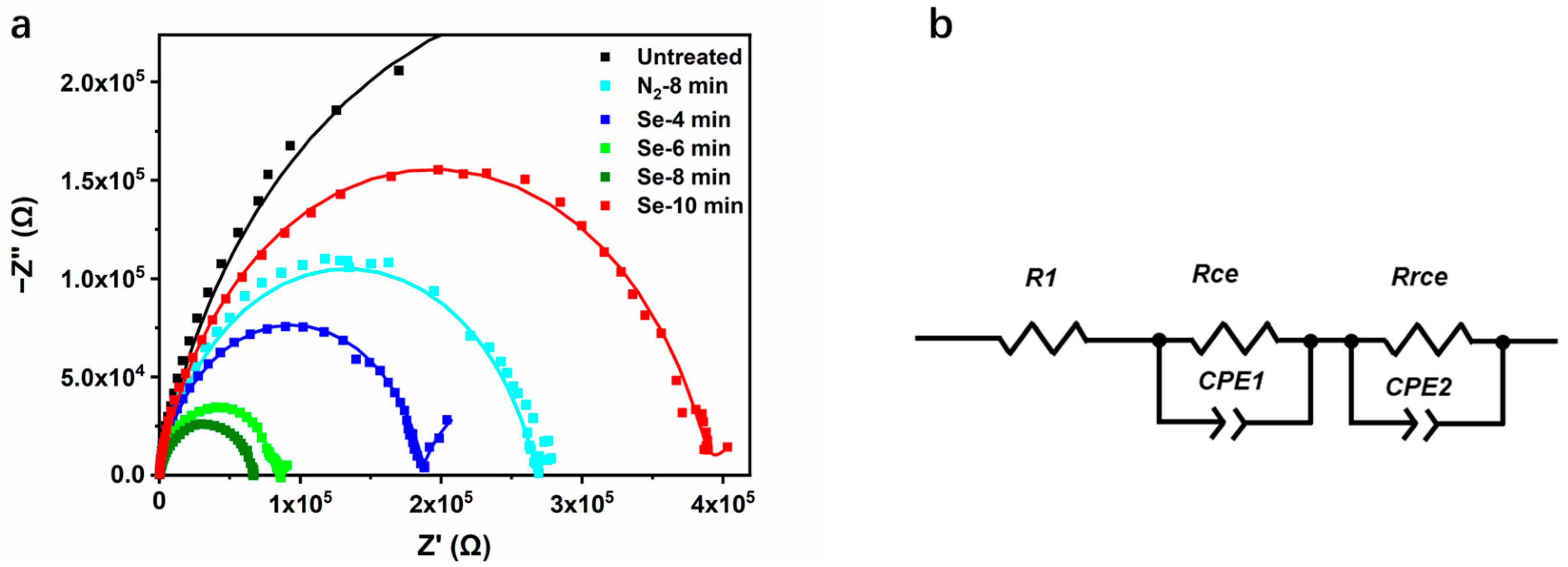
To further understand the effect of selenylation on the carrier dynamics, EIS measurements were carried out, and the results (Cole–Cole plots) in the frequency range 10 Hz to 1 MHz are shown in Figure 4a [30,31]. The plots of all devices exhibited a quasi-semicircle shape which could be divided by a high-frequency arc and a connected low-frequency arc. The Cole–Cole plots were analyzed using an equivalent circuit as shown in Figure 4b in which R1 represents the series resistance, shunt pair Rce and CPE1 are associated with CuSbS2(Se)/CdS interfaces, and shunt pair Rrce and CPE2 represents the carrier transport factor in CuSbS2(Se). CPE represents a capacitance-like element in the modeling for inhomogeneity in the interface, and is conventionally defined by two values, namely, CPE-T and CPE-P. CPE-T is capacitance, while CPE-P is a non-homogeneity constant. The results indicate that the plots are in reasonable concordance with the simulated curve (the solid line). All the parameters calculated from the fitted curve are summarized in Table 2.
It is well known that the series resistance is a factor that largely affects the photocurrent of a solar cell. For the untreated devices, the value of R1 is 265.7 Ω, and it significantly decreases to 58.7 Ω for the devices selenized for 8 min, corresponding to a substantial improvement of JSC, increasing from 1.41 to 4.70 mA cm−2. The devices selenized for 8 min also exhibit the lowest Rce, indicating their lower interfacial resistance. In contrast, the values of R1 and Rce remain as 212.5 Ω and 2.66 × 10⁵ Ω, respectively, and the JSC of devices show a very limited increase to 2.60 mA cm−2. Rrce, a characteristic parameter, reflects the recombination resistance [32]. A large value of Rrce represents that the device has a low carrier recombination rate. Notably, the Rrce of untreated devices is 0.8 × 10⁵ Ω and it increases to 1.2 × 10⁵ Ω and 8.1 × 10⁵ Ω after heated in N2 and Se vapor for 8 min, respectively. It indicates that the simple heat treatment has little effect on the carrier transport, and selenylation plays a more important role in reducing the carrier recombination. As previously discussed, the deep level crystal defects S vacancies (VS) constitute the dominant recombination centers that have profound effects on the electronic structure and carrier mobility of CuSbS2 film [29]. The density of VS obviously reduces as some Se gets into crystal lattice when it is selenized for a short time. However, when the selenylation duration is too long (≥10 min), the recombination rate increases sharply due to the short-circuit caused by the pinholes. The total carrier recombination rate for the devices could be reflected by a voltage-dependent time constant (τavg), which can be defined by the following equation [33]:
Table 2 summarizes that the τavg1 that is related to interface for 8 min-selenized devices is 0.60 ms, which is a little higher than that of the devices treated in N2. However, τavg2 that is related to carrier transport in CuSbS2 for 8 min-selenized devices is 33.88 s, which is much higher than that of the devices treated in N2 (3.80 s), indicating selenylation has a greater effect on the electronic properties of CuSbS2 film than CuSbS2(Se)/CdS interfaces.
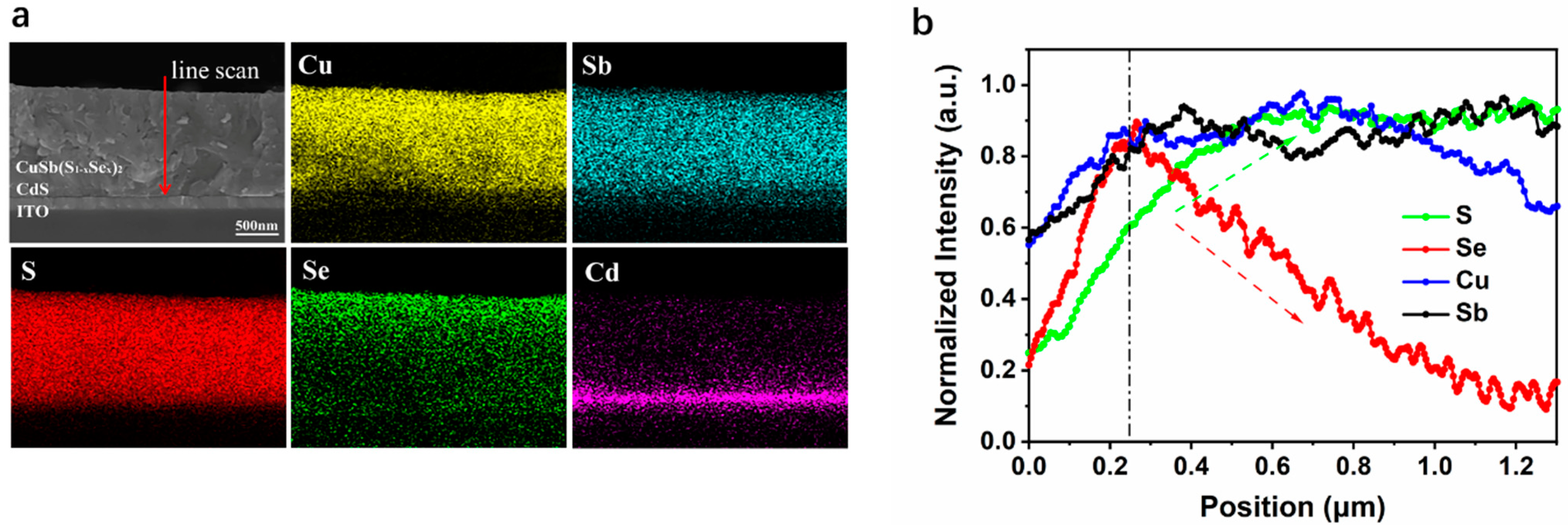
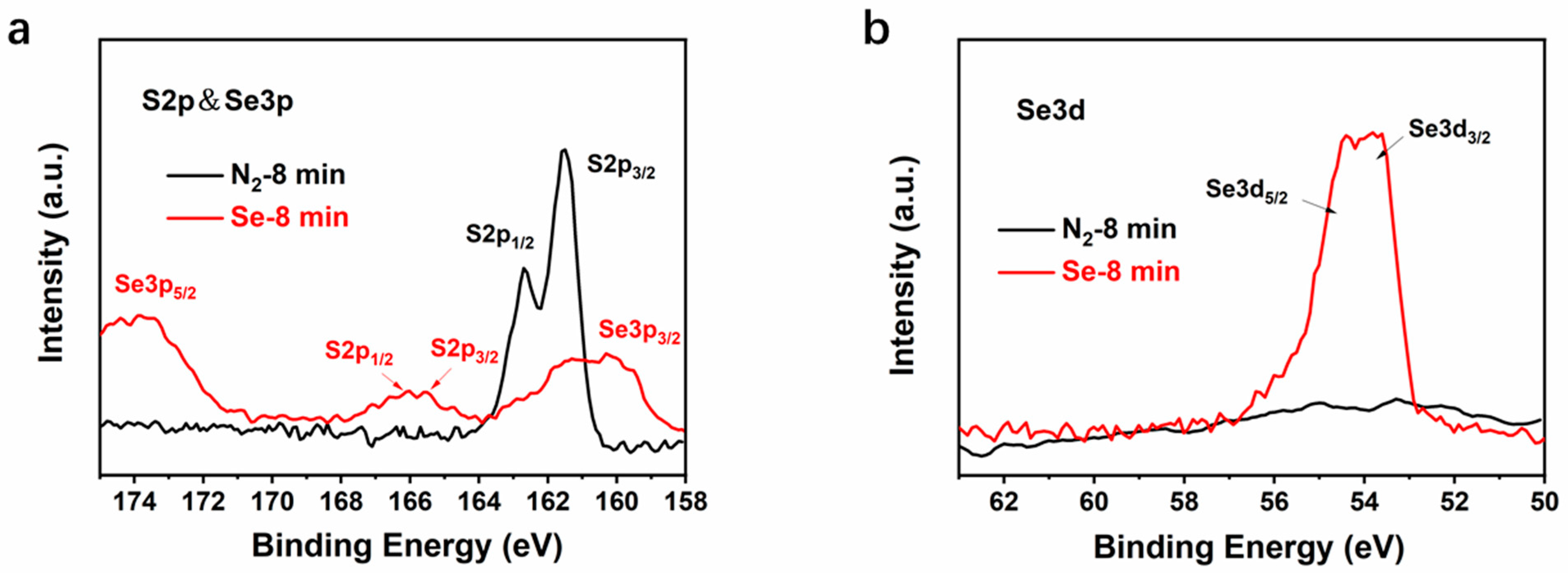
To further study the mechanism of selenylation and reveal the characteristics of reaction between Se and CuSbS2 films, quantitative elemental analysis was carried by X-ray energy dispersive spectroscopy (EDS). The global concentration of each element on CuSbS2(Se) films selenized for different durations was also analyzed. Table 3 summarizes the concentration and ratio of Cu, Sb, S, and Se, and the data corresponding to each element are the average of 6 test points. The results indicate that a small amount of Se (<1%) could be found in 4-min selenized film. The Se concentration increased gradually with the increase in the selenylation time to 10 min. When the selenylation duration was prolonged to 6 and 8 min, a lot of S element in CuSbS2 was substituted by Se. Moreover, the compositional ratio Se/(S + Se) reached 24% and 39%, confirming that CuSbS2 prepared by SPD method could easily react with Se vapor and transformed to CuSb(S,Se)2 at 400 °C. A cross-section view along with EDS elemental mapping results of 8-min selenized CuSbS2(Se) film is shown in Figure 5a. Figure 5b exhibits the line scanning results of S, Se, Cu, and Sb elements. The concentration of Se element decreases gradually from surface to deeper inside the film, while the concentration of S at near-surface is obviously lower than that in the inner body. It indicates that the most of S element was substituted with Se in the near surface of CuSbS2(Se) film, and the substituted rate reduced gradually with the increase in the diffusion length. The XPS spectra of S and Se provide another evidence, as shown in Figure 6a,b. For 8-min annealed CuSbS2 film, a sharp S2p XPS peak centered at 162 eV consisted of S2p1/2 and S2p3/2 could be well distinct. However, this peak became very weak even lower than those of Se3p1/2 and Se3p3/2 with an 8-min selenylation. Instead, the sharp Se3d XPS centered at 54.2 eV and consisting of S3p3/2 and S3p5/2, was easily found in 8-min selenized films, confirming the existence of few S elements in the near surface region. Significantly, the concentration of Se near the interface is less than 10%, which could explain why there is not much difference in photo-response range (Figure 3c) and why selenylation has a greater effect on the electronic properties of CuSbS2 film than CuSbS2(Se)/CdS interfaces (Se AC impedance analysis) for devices treated in N2 and Se vapor.
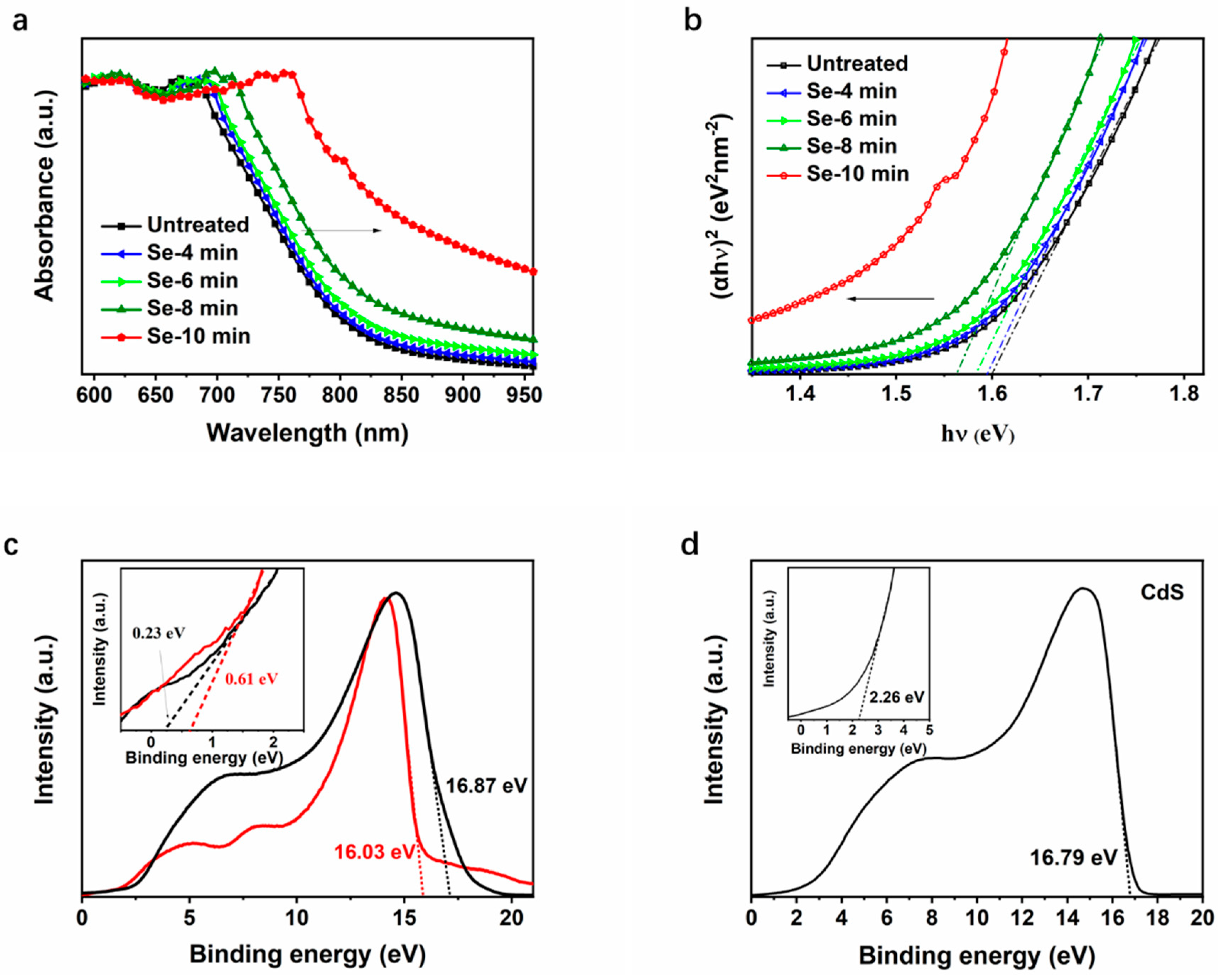
The effect of selenylation on the energy levels was subsequently investigated. Figure 6a shows the optical absorption spectra of absorbers heated in N2, and selenized for 4, 6, 8, and 10 min, respectively. Noteworthy, little difference is observed in absorption edges of the untreated film, film heated in N2, and films selenized for 4 min. The absorption spectra of films show a gradual red shift toward a longer wavelength with an increase in the selenylation duration. For the film selenized for 10 min, a much broader absorption is observed in the 800–950 nm range. Usually, the direct energy band gap (Eg) of could be calculated by using the following formula [34]:
with A is a constant, h is the Planck’s constant, and ν is the frequency of the incident photon. Figure 5 demonstrates that selenized CuSbS2 films belong to multiphase film, which could not be described by applying this formula in a strict sense. However, the Eg of CuSbS2(Se) could also be roughly estimated by using this formula by UV–vis absorption spectroscopy (Figure 7a) and model the linear zone of (αhν)2 versus (hν) when it was lightly selenized, as shown in Figure 7b. The untreated sample shows an Eg of 1.60 eV, which slightly increases to 1.58 eV as it heated in N2. The average Eg of CuSbS2(Se) decreased to 1.56 eV when it was selenized for 8 min. For the film selenized for 10 min, no linear zone could be fitted appropriately. However, undoubtedly, the average Eg is much lower than that for the film selenized for 10 min according to the variation trend. It indicates that, as a photovoltaic absorber, CuSbS2(Se) needs a longer selenylation time to create a suitable Eg to utilize more sunlight in the near-IR region. Currently, the problems such as improvement in the prevention of the appearance of pinholes or to find an effective passivation approach require urgent solutions.
UPS was used to further depict the energy level of CuSbS2(Se) [13,35]. The UPS spectra of CuSbS2 film heated in N2 and CuSbS2(Se) film selenized for 8 min are shown in Figure 7c. The UPS spectrum for CdS is shown in Figure 7d. The work function (WF), conduction band minimum (EC), and valence band maximum (EV) were determined based on the valence band onset (VBO) and cut-off region (Ecutoff) of the UPS spectrum, and the results are listed in Table 4. Clearly, the VBO of CuSbS2 film heated in N2 is 0.27 eV, and it increases to 0.61 eV when selenized for 8 min. The WF of CuSbS2 film heated in N2 is 4.34 eV, and it increases to 5.03 eV after selenylation. It can be concluded that the surface state and energy level of selenized CuSbS2 has been modified and would bring some effect on the carrier transport.
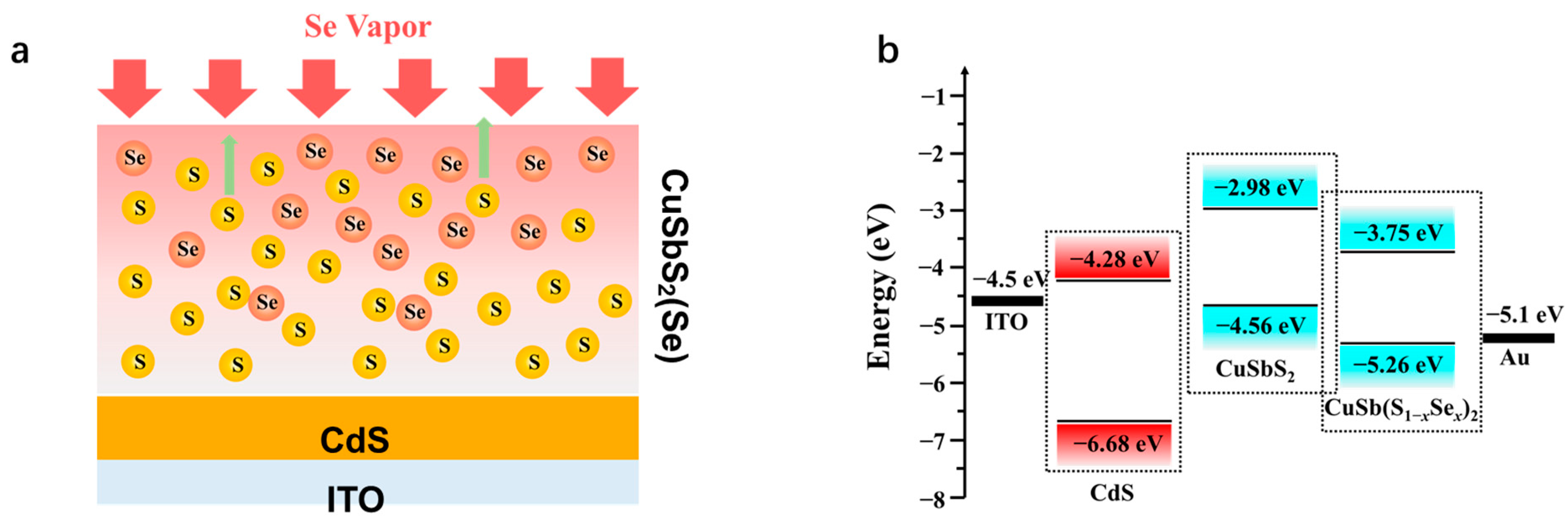
As discussed earlier, the concentration of Se element gradient decreases from top to the deeper positions, and the corresponding distribution process is depicted in Figure 8a. For a lightly selenized CuSbS2(Se) absorber, the practical structure of device could be written as ITO/CdS/CuSbS2/CuSbS2(Se)/Au. Combining the results of UV–vis spectra and UPS analysis, the energy level of CdS/CuSbS2/CuSbS2(Se) p-i-n junction could be easily confirmed, as shown in Figure 8b. Notably, the EC and EV of CuSbS2(Se) are −3.75 eV and −5.26 eV, respectively, which are slightly lower than those of CuSbS2 and match better with the CdS buffer layer. The CuSbS2(Se)/CdS has a lower energy barrier for both holes and free electrons transport to anode and cathode, respectively. However, little Se could distribute to the interface of p–n junction in a short selenylation duration; therefore, CuSbS2 inevitably exists between CuSbS2(Se) and CdS. Both holes and free electrons would be blocked more or less by the CuSbS2 layer during their transport process. Thus, to further improve the performance of CdS/CuSbS2 solar cells, the CuSbS2 layer should be reduced to the maximum extent in order to avoid the destruction of the film structure.
4. Conclusions
In this study, CuSbS2(Se) films with a high Se substitution rate (~39%) were successfully prepared using porous CuSbS2 films deposited by spray pyrolysis followed by a post-treatment in Se vapor. The CuSbS2 device shows a significant improvement from 0.12% to 0.90%. Two major findings were concluded: First, selenylation leads to an obvious reduction of the carrier recombination center, which is related to deep-level VS and antisite defects created by the loss of S during processing. Second, selenylation leads to the modification of the band structure and energy level of CuSbS2 films. The average Eg decreases from 1.58 to below 1.51 eV, and the EC and EV decrease from −2.98 and −4.56 eV to −3.75 and −5.26 eV, respectively, accompanied by a reduction of the energy barrier for both holes and free electrons transport to anode and cathode, respectively. Moreover, elemental analysis results reveal a gradient distribution for Se from the top surface to the deep region. Unselenized CuSbS2 layer existing in CuSbS2(Se) has some bad effect on the carrier transport. Thus, in order to further improve the performance of CdS/CuSbS2 solar cells, a more sufficient selenylation should be carried out and CuSbS2 layer should be reduced as much as possible. Undeniably, a lot more systematic explorations are still demanded to investigate an efficient selenylation technique that would not destroy the structure of the CuSbS2 films, which will be pursued in the future work.
Author Contributions
Writing—original draft, M.Z.; conceptualization, methodology, investigation, J.Y.; formal analysis, validation, L.F.; characterization, data curation, Y.G.; supervision, writing—review & editing, H.T.; resources, funding acquisition L.L.; writing—review & editing, J.C. All authors have read and agreed to the published version of the manuscript.
Funding
This study was supported by the National Key Research and Development Project of China (Grant No. 2018YFB0407102), Sichuan Province Key Laboratory of Display Science and Technology (ZYGX2022K018), the Program of Chongqing Science & Technology Commission (cstc2018jscxmsybX0099, cstc2019jcyj-msxmX0877), Financial Projects of Sichuan Science and Technology Department (2018ZYZF0062), Scientific and Technological Research Program of Chongqing Municipal Education Commission (KJZD-K201901302, KJQN201901348, KJCX2020048), and Public Service Platform for The Industrialization of Technological Innovation Achievements in the Field of Robot and Intelligent Manufacturing in Chongqing (2019-00900-1-1).
Institutional Review Board Statement
Not applicable.
Informed Consent Statement
Not applicable.
Data Availability Statement
The data presented in this study are available on a reasonable request from the corresponding author.
Conflicts of Interest
The authors declare no conflict of interest.
References
- Sadanand; Dwivedi, D.K. Modeling of Photovoltaic Solar Cell Based on CuSbS2 Absorber for the Enhancement of Performance. IEEE Trans. Electron Devices 2021, 68, 1121–1128. [Google Scholar] [CrossRef]
- Chen, S.; Liu, T.; Zheng, Z.; Ishaq, M.; Liang, G.; Fan, P.; Chen, T.; Tang, J. Recent progress and perspectives on Sb2Se3-based photocathodes for solar hydrogen production via photoelectrochemical water splitting. J. Energy Chem. 2021, in press. [Google Scholar] [CrossRef]
- Jackson, P.; Hariskos, D.; Wuerz, R.; Kiowski, O.; Bauer, A.; Friedlmeier, T.M.; Powalla, M. Properties of Cu(In,Ga)Se2 solar cells with new record efficiencies up to 21.7%. Phys. Status Solidi (RRL) Rapid Res. Lett. 2015, 9, 28–31. [Google Scholar] [CrossRef]
- Green, M.A.; Emery, K.; Hishikawa, Y.; Warta, W.; Dunlop, E.D. Solar cell efficiency tables (version 47). Prog. Photovolt. Res. Appl. 2016, 24, 3–11. [Google Scholar] [CrossRef]
- Jeong, J.; Kim, M.; Seo, J.; Lu, H.; Ahlawat, P.; Mishra, A.; Yang, Y.; Hope, M.A.; Eickemeyer, F.T.; Kim, M.; et al. Pseudo-halide anion engineering for α-FAPbI3 perovskite solar cells. Nat. Cell Biol. 2021, 592, 381–385. [Google Scholar] [CrossRef]
- Yoo, J.J.; Seo, G.; Chua, M.R.; Park, T.G.; Lu, Y.; Rotermund, F.; Kim, Y.-K.; Moon, C.S.; Jeon, N.J.; Correa-Baena, J.-P.; et al. Efficient perovskite solar cells via improved carrier management. Nat. Cell Biol. 2021, 590, 587–593. [Google Scholar] [CrossRef]
- Wang, J.; Zheng, Z.; Zu, Y.; Wang, Y.; Liu, X.; Zhang, S.; Zhang, M.; Hou, J. A Tandem Organic Photovoltaic Cell with 19.6% Efficiency Enabled by Light Distribution Control. Adv. Mater. 2021, 33, 2102787. [Google Scholar] [CrossRef]
- Chen, S.; Ishaq, M.; Xiong, W.; Shah, U.A.; Farooq, U.; Luo, J.; Zheng, Z.; Su, Z.; Fan, P.; Zhang, X.; et al. Improved Open-Circuit Voltage of Sb2Se3 Thin-Film Solar Cells Via Interfacial Sulfur Diffusion-Induced Gradient Bandgap Engineering. Sol. RRL 2021, 5, 2100419. [Google Scholar] [CrossRef]
- Tao, J.; Hu, X.; Guo, Y.; Hong, J.; Li, K.; Jiang, J.; Chen, S.; Jing, C.; Yue, F.; Yang, P.; et al. Solution-processed SnO2 interfacial layer for highly efficient Sb2Se3 thin film solar cells. Nano Energy 2019, 60, 802–809. [Google Scholar] [CrossRef]
- Han, J.; Wang, S.; Yang, J.; Guo, S.; Cao, Q.; Tang, H.; Pu, X.; Gao, B.; Li, X. Solution-Processed Sb2S3 Planar Thin Film Solar Cells with a Conversion Efficiency of 6.9% at an Open Circuit Voltage of 0.7 V Achieved via Surface Passivation by a SbCl3 Interface Layer. ACS Appl. Mater. Interfaces 2019, 12, 4970–4979. [Google Scholar] [CrossRef]
- Wang, K.; Cheng, J.; Yang, X.; Hu, R.; Fu, L.; Huang, J.; Yu, J.; Li, L. Enhanced Photovoltaic Properties in Sb2S3 Planar Heterojunction Solar Cell with a Fast Selenylation Approach. Nanoscale Res. Lett. 2018, 13, 270. [Google Scholar] [CrossRef]
- Pan, Y.; Hu, X.; Guo, Y.; Pan, X.; Zhao, F.; Weng, G.; Tao, J.; Zhao, C.; Jiang, J.; Chen, S.; et al. Vapor Transport Deposition of Highly Efficient Sb2(S,Se)3 Solar Cells via Controllable Orientation Growth. Adv. Funct. Mater. 2021, 31, 2101476. [Google Scholar] [CrossRef]
- Wang, X.; Tang, R.; Jiang, C.; Lian, W.; Ju, H.; Jiang, G.; Li, Z.; Zhu, C.; Chen, T. Manipulating the Electrical Properties of Sb2(S,Se)3 Film for High-Efficiency Solar Cell. Adv. Energy Mater. 2020, 10, 2002341. [Google Scholar] [CrossRef]
- Tang, R.; Wang, X.; Lian, W.; Huang, J.; Wei, Q.; Huang, M.; Yin, Y.; Jiang, C.; Yang, S.; Xing, G.; et al. Hydrothermal deposition of antimony selenosulfide thin films enables solar cells with 10% efficiency. Nat. Energy 2020, 5, 587–595. [Google Scholar] [CrossRef]
- Sadanand; Singh, P.K.; Rai, S.; Lohia, P.; Dwivedi, D. Comparative study of the CZTS, CuSbS2 and CuSbSe2 solar photovoltaic cell with an earth-abundant non-toxic buffer layer. Sol. Energy 2021, 222, 175–185. [Google Scholar] [CrossRef]
- Wen, X.; Chen, C.; Lu, S.; Li, K.; Kondrotas, R.; Zhao, Y.; Chen, W.; Gao, L.; Wang, C.; Zhang, J.; et al. Vapor transport deposition of antimony selenide thin film solar cells with 7.6% efficiency. Nat. Commun. 2018, 9, 1–10. [Google Scholar] [CrossRef] [PubMed]
- Li, Z.; Liang, X.; Li, G.; Liu, H.; Zhang, H.; Guo, J.; Chen, J.; Shen, K.; San, X.; Yu, W.; et al. 9.2%-efficient core-shell structured antimony selenide nanorod array solar cells. Nat. Commun. 2019, 10, 1–9. [Google Scholar] [CrossRef] [PubMed] [Green Version]
- Gupta, G.K.; Dixit, A. Simulation studies on photovoltaic response of ultrathin CuSb(S,Se)2 ternary compound semiconductors absorber-based single junction solar cells. Int. J. Energy Res. 2020, 44, 3724–3736. [Google Scholar] [CrossRef]
- Krishnan, B.; Shaji, S.; Ornelas, R.E. Progress in development of copper antimony sulfide thin films as an alternative material for solar energy harvesting. J. Mater. Sci. Mater. Electron. 2015, 26, 4770–4781. [Google Scholar] [CrossRef]
- Welch, A.W.; Baranowski, L.L.; Zawadzki, P.; Lany, S.; Wolden, C.A.; Zakutayev, A. CuSbSe2 photovoltaic devices with 3% efficiency. Appl. Phys. Express 2015, 8, 82301. [Google Scholar] [CrossRef] [Green Version]
- de Souza Lucas, F.W.; Welch, A.W.; Baranowski, L.L.; Dippo, P.C.; Hempel, H.; Unold, T.; Eichberger, R.; Blank, B.; Rau, U.; Mascaro, L.; et al. Effects of Thermochemical Treatment on CuSbS2 Photovoltaic Absorber Quality and Solar Cell Reproducibility. J. Phys. Chem. C 2016, 120, 18377–18385. [Google Scholar] [CrossRef]
- Fu, L.; Yu, J.; Wang, J.; Xie, F.; Yao, S.; Zhang, Y.; Cheng, J.; Li, L. Thin film solar cells based on Ag-substituted CuSbS2 absorber. Chem. Eng. J. 2020, 400, 125906. [Google Scholar] [CrossRef]
- Cheng, J.; Hu, R.; Wang, K.; Meng, X.; Li, Y.; Yang, X.; Liao, X.; Li, L.; Chong, K.B. Air-Stable Solar Cells with 0.7 V Open-Circuit Voltage Using Selenized Antimony Sulfide Absorbers Prepared by Hydrazine-Free Solution Method. Sol. RRL 2019, 3, 1800346. [Google Scholar] [CrossRef]
- Xie, F.; Tang, H.; Zhao, X.; Li, M.; Li, L.; Cheng, J. Thin-Film Solar Cells using a Selenized Silver Antimony Sulfide Absorber Prepared by Spray Pyrolysis Deposition. Phys. Status Solidi (RRL) Rapid Res. Lett. 2021, 2000514. [Google Scholar] [CrossRef]
- Zhang, Y.; Li, J.; Jiang, G.; Liu, W.; Yang, S.; Zhu, C.; Chen, T. Selenium-Graded Sb2(S1−xSex)3 for Planar Heterojunction Solar Cell Delivering a Certified Power Conversion Efficiency of 5.71%. Sol. RRL 2017, 1, 1700017. [Google Scholar] [CrossRef]
- Yao, S.; Wang, J.; Cheng, J.; Fu, L.; Xie, F.; Zhang, Y.; Li, L. Improved Performance of Thermally Evaporated Sb2Se3 Thin-Film Solar Cells via Substrate-Cooling-Speed Control and Hydrogen-Sulfide Treatment. ACS Appl. Mater. Interfaces 2020, 12, 24112–24124. [Google Scholar] [CrossRef]
- Liang, G.-X.; Zheng, Z.-H.; Fan, P.; Luo, J.-T.; Hu, J.-G.; Zhang, X.-H.; Ma, H.-L.; Fan, B.; Luo, Z.-K.; Zhang, D.-P. Thermally induced structural evolution and performance of Sb2Se3 films and nanorods prepared by an easy sputtering method. Sol. Energy Mater. Sol. Cells 2018, 174, 263–270. [Google Scholar] [CrossRef]
- Luo, Y.-D.; Tang, R.; Chen, S.; Hu, J.-G.; Liu, Y.-K.; Li, Y.-F.; Liu, X.-S.; Zheng, Z.-H.; Su, Z.-H.; Ma, X.-F.; et al. An effective combination reaction involved with sputtered and selenized Sb precursors for efficient Sb2Se3 thin film solar cells. Chem. Eng. J. 2020, 393, 124599. [Google Scholar] [CrossRef]
- Liang, G.-X.; Luo, Y.-D.; Chen, S.; Tang, R.; Zheng, Z.-H.; Li, X.-J.; Liu, X.-S.; Liu, Y.-K.; Li, Y.-F.; Chen, X.-Y.; et al. Sputtered and selenized Sb2Se3 thin-film solar cells with open-circuit voltage exceeding 500 mV. Nano Energy 2020, 73, 104806. [Google Scholar] [CrossRef]
- Naveena, D.; Thirumalaisamy, L.; Dhanabal, R.; Sethuraman, K.; Bose, A.C. Tuning the Properties of the CuAl(1–x)FexS2 Thin Film as a Potential Absorber for Solar Cell Application. ACS Appl. Energy Mater. 2020, 3, 10550–10559. [Google Scholar] [CrossRef]
- Wang, X.; Tang, R.; Yin, Y.; Ju, H.; Li, S.; Zhu, C.; Chen, T. Interfacial engineering for high efficiency solution processed Sb2Se3 solar cells. Sol. Energy Mater. Sol. Cells 2019, 189, 5–10. [Google Scholar] [CrossRef]
- Wang, W.; Wang, X.; Chen, G.; Chen, B.; Cai, H.; Chen, T.; Chen, S.; Huang, Z.; Zhu, C.; Zhang, Y. Promising Sb2(S,Se)3 Solar Cells with High Open Voltage by Application of a TiO2/CdS Double Buffer Layer. Sol. RRL 2018, 2, 1800208. [Google Scholar] [CrossRef]
- Cheng, J.; Wang, S.; Tang, Y.; Hu, R.; Yan, X.; Zhang, Z.; Li, L.; Pei, Q. Intensification of Vertical Phase Separation for Efficient Polymer Solar Cell via Piecewise Spray Assisted by a Solvent Driving Force. Sol. RRL 2020, 4, 1900458. [Google Scholar] [CrossRef]
- Ren, D.; Luo, X.; Chen, S.; Zheng, Z.; Cathelinaud, M.; Liang, G.; Ma, H.; Qiao, X.; Fan, X.; Zhang, X. Structure, Morphology, and Photoelectric Performances of Te-Sb2Se3 Thin Film Prepared via Magnetron Sputtering. Nanomaterials 2020, 10, 1358. [Google Scholar] [CrossRef] [PubMed]
- Tang, R.; Zheng, Z.-H.; Su, Z.-H.; Li, X.-J.; Wei, Y.-D.; Zhang, X.-H.; Fu, Y.-Q.; Luo, J.-T.; Fan, P.; Liang, G.-X. Highly efficient and stable planar heterojunction solar cell based on sputtered and post-selenized Sb2Se3 thin film. Nano Energy 2019, 64, 103929. [Google Scholar] [CrossRef]
Figure 1.
Crystal structure and composition analysis: (a) XRD analysis of the untreated film, and films annealed in N2 and Se vapor and (b) Magnified XRD peaks of the annealed film and films selenized for 4, 6, and 8 min.
Figure 1.
Crystal structure and composition analysis: (a) XRD analysis of the untreated film, and films annealed in N2 and Se vapor and (b) Magnified XRD peaks of the annealed film and films selenized for 4, 6, and 8 min.

Figure 2.
Analysis of surface morphologies of CuSbS2 film: SEM micrographs of (a) the untreated film, (b) film annealed in N2 for 8 min, and selenized films for (c) 4 min, (d) 6 min, (e) 8 min, and (f) 10 min.
Figure 2.
Analysis of surface morphologies of CuSbS2 film: SEM micrographs of (a) the untreated film, (b) film annealed in N2 for 8 min, and selenized films for (c) 4 min, (d) 6 min, (e) 8 min, and (f) 10 min.

Figure 3.
Performance test of the devices based on CuSbS2 and CuSbS2(Se): (a) the structure of CuSbS2(Se) solar cells; (b) J–V characteristics under illumination, (c) EQE, (d) J–V characteristics in dark of CuSbS2 device and CuSbS2(Se) devices selenized for different durations; (e) shunt conductance G characterizations, (f) ideality factor A and reverse saturation current density J0 characterizations.

Figure 4.
ESI analysis: (a) Cole–Cole plots and (b) equivalent circuit model of CuSbS2 and CuSbS2 (Se) devices. The solid lines represent the fitted results.
Figure 4.
ESI analysis: (a) Cole–Cole plots and (b) equivalent circuit model of CuSbS2 and CuSbS2 (Se) devices. The solid lines represent the fitted results.

Figure 5.
Quantitative elemental analysis: (a) EDS elemental mapping and (b) Element distribution in CuSbS2(Se) selenized for 8 min.
Figure 5.
Quantitative elemental analysis: (a) EDS elemental mapping and (b) Element distribution in CuSbS2(Se) selenized for 8 min.

Figure 6.
XPS analysis: Core level spectra of (a) S2p and Se3p and (b) Se3d of CuSbS2 and CuSbS2(Se) selenized for 8 min.
Figure 6.
XPS analysis: Core level spectra of (a) S2p and Se3p and (b) Se3d of CuSbS2 and CuSbS2(Se) selenized for 8 min.

Figure 7.
Optical properties and energy level analysis of CuSbS2 and CuSbS2 film: (a) UV–vis absorption spectra, (b) plots of (αhν)2 versus (hν); and UPS spectra of (c) CuSbS2(Se) selenized for 8 and 10 min and (d) CdS spectrum.
Figure 7.
Optical properties and energy level analysis of CuSbS2 and CuSbS2 film: (a) UV–vis absorption spectra, (b) plots of (αhν)2 versus (hν); and UPS spectra of (c) CuSbS2(Se) selenized for 8 and 10 min and (d) CdS spectrum.

Figure 8.
Energy band structure analysis of CdS/CuSbS2(Se): (a) a sketch of Se distribution in CuSbS2(Se) and (b) energy level of CdS/CuSbS2(Se) heterojunction interface.
Figure 8.
Energy band structure analysis of CdS/CuSbS2(Se): (a) a sketch of Se distribution in CuSbS2(Se) and (b) energy level of CdS/CuSbS2(Se) heterojunction interface.


Table 1.
The detailed photovoltaic parameters of CuSbS2 and CuSbS2 (Se) solar cells selenized for varied durations.
Table 1.
The detailed photovoltaic parameters of CuSbS2 and CuSbS2 (Se) solar cells selenized for varied durations.
| Sample | VOC (V) | JSC (mA cm−2) | FF | PCE (%) |
|---|---|---|---|---|
| Untreated | 0.31 ± 0.02 | 1.41 ± 0.24 | 0.28 ± 0.03 | 0.12 ± 0.06 |
| A-8 min | 0.54 ± 0.01 | 2.60 ± 0.14 | 0.32 ± 0.02 | 0.46 ± 0.05 |
| Se-4 min | 0.35 ± 0.01 | 2.83 ± 0.32 | 0.30 ± 0.03 | 0.28 ± 0.07 |
| Se-6 min | 0.47 ± 0.01 | 3.70 ± 0.35 | 0.32 ± 0.03 | 0.57 ± 0.12 |
| Se-8 min | 0.48 ± 0.02 | 4.70 ± 0.41 | 0.39 ± 0.02 | 0.90 ± 0.14 |
| Se-10 min | 0.42 ± 0.04 | 2.00 ± 0.46 | 0.34 ± 0.04 | 0.31 ± 0.17 |
Table 2.
Calculation parameters from the fitted impedance spectra.
| Circuit Element | Sample | |||||
|---|---|---|---|---|---|---|
| Untreated | N2-8 min | Se-4 min | Se-6 min | Se-8 min | Se-10 min | |
| R1 (Ω) | 265.7 | 219.7 | 212.5 | 112.5 | 58.7 | 178.5 |
| Rce (Ω) | 6.17 × 10⁵ | 2.66 × 10⁵ | 1.87 × 10⁵ | 0.82 × 10⁵ | 0.66 × 10⁵ | 3.87 × 10⁵ |
| CPE1-T (F cm−2) | 0.23 × 10⁻⁹ | 1.32 × 10⁻⁹ | 1.61 × 10⁻⁹ | 6.81 × 10⁻⁹ | 9.12 × 10⁻⁹ | 0.78 × 10⁻⁹ |
| τavg1 (S) | 1.42 × 10⁻⁴ | 3.51 × 10⁻⁴ | 3.01 × 10⁻⁴ | 5.58 × 10⁻⁴ | 6.01 × 10⁻⁴ | 3.01 × 10⁻⁴ |
| CPE1-P | 0.85 | 0.90 | 0.87 | 0.90 | 0.91 | 0.86 |
| Rrce (Ω) | 0.8 × 10⁵ | 1.2 × 10⁵ | 1.0 × 10⁵ | 5.5 × 10⁵ | 8.1 × 10⁵ | 4.3 × 10⁵ |
| CPE2-T (F cm−2) | 1.52 × 10⁻⁵ | 3.17 × 10⁻⁵ | 5.58 × 10⁻⁵ | 6.16 × 10⁻⁵ | 7.06 × 10⁻⁵ | 2.38 × 10⁻⁵ |
| τavg2 (S) | 1.216 | 3.80 | 5.58 | 33.88 | 57.186 | 10.234 |
| CPE2-P | 0.93 | 0.93 | 0.94 | 0.94 | 0.96 | 0.89 |
Table 3.
Global elemental analysis of Cu, Sb, S, and Se elements in CuSbS2(Se) samples selenized for different durations.
Table 3.
Global elemental analysis of Cu, Sb, S, and Se elements in CuSbS2(Se) samples selenized for different durations.
| Sample | Composition (at.%) | Compositional Ratio (%) | |||||
|---|---|---|---|---|---|---|---|
| Cu | Sb | S | Se | S/(S + Se) | Se/(S + Se) | (S + Se)/(Cu + Sb) | |
| Untreated | 25.69 | 25.54 | 48.77 | 0 | 1 | 0 | 0.95 |
| Se-4 min | 25.44 | 25.28 | 49.22 | 0.06 | 1 | 0 | 0.97 |
| Se-6 min | 25.43 | 25.17 | 46.33 | 2.77 | 0.94 | 0.06 | 0.97 |
| Se-8 min | 25.27 | 25.16 | 37.92 | 11.65 | 0.76 | 0.24 | 0.98 |
| Se-10 min | 25.57 | 25.30 | 29.92 | 19.21 | 0.61 | 0.39 | 0.97 |
Table 4.
Parameters calculated from the UPS spectra.
| Sample | Eg (eV) | VBO (eV) | WF (eV) | EC (eV) | EV (eV) |
|---|---|---|---|---|---|
| CuSbS2 | 1.58 | 0.27 | 4.34 | −2.98 | −4.56 |
| CuSbS2(Se) | 1.51 | 0.61 | 5.03 | −3.75 | −5.26 |
| CdS | 2.4 | 2.26 | 4.42 | −4.28 | −6.68 |
Publisher’s Note: MDPI stays neutral with regard to jurisdictional claims in published maps and institutional affiliations. |
© 2021 by the authors. Licensee MDPI, Basel, Switzerland. This article is an open access article distributed under the terms and conditions of the Creative Commons Attribution (CC BY) license (https://creativecommons.org/licenses/by/4.0/).
Share and Cite
MDPI and ACS Style
Zhao, M.; Yu, J.; Fu, L.; Guan, Y.; Tang, H.; Li, L.; Cheng, J. Thin-Film Solar Cells Based on Selenized CuSbS2 Absorber. Nanomaterials 2021, 11, 3005. https://0-doi-org.brum.beds.ac.uk/10.3390/nano11113005
AMA Style
Zhao M, Yu J, Fu L, Guan Y, Tang H, Li L, Cheng J. Thin-Film Solar Cells Based on Selenized CuSbS2 Absorber. Nanomaterials. 2021; 11(11):3005. https://0-doi-org.brum.beds.ac.uk/10.3390/nano11113005
Chicago/Turabian StyleZhao, Minghao, Junsheng Yu, Lijuan Fu, Youwei Guan, Hua Tang, Lu Li, and Jiang Cheng. 2021. "Thin-Film Solar Cells Based on Selenized CuSbS2 Absorber" Nanomaterials 11, no. 11: 3005. https://0-doi-org.brum.beds.ac.uk/10.3390/nano11113005
Note that from the first issue of 2016, this journal uses article numbers instead of page numbers. See further details here.